
 Open Access Article
 This Open Access Article is licensed under a Creative Commons Attribution-Non Commercial 3.0 Unported Licence
Crystal structure of a large cubic tin monosulfide polymorph: an unraveled puzzle†
R. E.
Abutbul
ab,
A. R.
Garcia-Angelmo
c,
Z.
Burshtein
a,
M. T. S.
Nair
c,
P. K.
Nair
*c and
Y.
Golan
*ab
aDepartment of Materials Engineering, Ben-Gurion University of the Negev, Beer-Sheva 84105, Israel. E-mail: ygolan@bgu.ac.il
bIlse Katz Institute for Nanoscale Science and Technology, Ben-Gurion University of the Negev, Beer-Sheva 84105, Israel
cInstituto de Energías Renovables, Universidad Nacional Autónoma de México, Temixco 62580, Morelos, Mexico. E-mail: pkn@ier.unam.mx
First published on 19th May 2016
Abstract
We present the atomic arrangement of 64 atoms within a simple cubic unit cell crystalline structure of lattice constant 11.6 Å, observed in tin sulfide (SnS) thin films. Thin films of 260 or 550 nm in thickness were deposited at 17 °C from a chemical bath containing tin(II) chloride and thioacetamide. The X-ray diffraction (XRD) patterns of these thin films are consistent with those of a simple cubic structure of lattice constant 11.600 ± 0.025 Å (as-prepared) or 11.603 ± 0.007 Å (after 400 °C heating). The said recently discovered “π-SnS” structure was adopted from previous reports, using the present, newly acquired experimental data to obtain the atomic positions. This structural assignment unravels a puzzle originated by inconsistencies among the XRD patterns of some SnS thin films and nanocrystals prepared via certain chemical routes, and the zinc blende, rock salt or pseudo-tetragonal structures previously assigned to them. In addition to its relevance as a stable solar cell material, salient features of this SnS polymorph arising from its lack of centro-symmetry are discussed.
Introduction
Large unit cell simple cubic tin sulfide is a polymorph of SnS, unrecognized prior to our 2015–2016 reports.1–3 Based on precession electron diffraction patterns (PED) of nanocrystals,1 this new crystalline phase was termed π-SnS, and based on X-ray diffraction (XRD) patterns of chemically deposited thin films,3 it was termed SnS-CUB. This cubic unit cell of lattice constant a = 11.6 Å is “large” compared with that of the naturally occurring orthorhombic (ORT) polymorph (herzenbergite mineral; a = 4.329, b = 11.192, and c = 3.984 Å) given in the powder diffraction file (PDF 39-0354)4 or that of epitaxial SnS thin films of rock-salt (RS) structure (a = 5.80 ± 0.02 Å) given in PDF 77-3356.5 Unit cells of these structures contain 8 atoms (4 × SnS), whereas the large simple cube contains 64 atoms (32 × SnS), per unit cell. In this work we illustrate that π-SnS and SnS-CUB are in fact identical. The present work is particularly relevant to the use of tin sulfide thin films as solar cell materials. In 2014, energy conversion efficiency approaching 4% was reported in solar cells using SnS-ORT.6 In 2015, SnS-CUB solar cells reached 1.28% efficiency, with an open circuit voltage Voc = 470 mV,7 which is nearly 100 mV larger than that of SnS-ORT solar cells (Voc = 370 mV). SnS-CUB solar cells are stable under concentrated sunlight (5 suns). Simultaneous use of SnS-ORT of optical band gap Eg = 1.07 eV and SnS-CUB of Eg = 1.7 eV has been proposed to improve their prospects in solar cell applications.3 It is pertinent to mention that the large simple cubic polymorph should have been recognized in hydrothermally prepared nanocrystals of SnS in the 2006 report.8 The same pertains to the chemically deposited SnS thin films reported in 2007 and 2008.9,10 Based on the relative XRD peak intensity ratios, those materials were initially considered to belong to the zinc blende (SnS-ZB) structure and not to the rock-salt (SnS-RS) structure known for this material since the 1960s.5 The unaccounted for diffraction peaks in the XRD pattern were assigned to SnS-ORT. The SnS-ZB structure assignment, however, met with a difficulty; it was found to be thermodynamically unstable in density functional theory (DFT) studies.11,12 A pseudo-tetragonal structure could explain some of the discrepancies,13 but it could not account for one important feature in the XRD pattern of SnS-CUB: a “triple peak signature”.3 This signature is present in all cases of SnS-CUB, irrespective of the chosen chemical preparation route,3,14 including a recently reported phase-selective chemical vapor deposition at 300 °C for SnS-ZB.15 The “thermodynamic instability” encountered in DFT studies was contentious because the triple-peak signature for both nanocrystals8 and thin films10 was found stable after heating the materials at 350 °C – the electron diffraction of the nanocrystal and the XRD pattern of thin film remained unchanged.These discrepancies got sorted out when a large simple cubic structure for SnS was proposed for the first time in 2015.1 It could equally account for the electron and X-ray diffraction patterns.2 Recent DFT stability calculations showed that SnS-CUB is a stable phase, as experimentally observed. In this work, we present the issues prevalent in the structural assignment for SnS-CUB thin films based on their XRD patterns, and then proceed to assign the atomic positions to Sn and S sites within the 64-atom-containing cubic cell.
Experimental
Deposition of tin sulfide thin films (SnS-CUB) was carried out on glass substrates at 17 °C using the chemical bath formulation reported in ref. 3 and 7. Films of 260 nm in thickness were deposited in two successive depositions, each lasting 10 h, while films of 550 nm in thickness were obtained by using four successive depositions. The films were compact, specularly reflective, and appeared reddish and deep red at thicknesses of 260 nm and 550 nm, respectively, in transmitted daylight. Corning microscope glass slides (75 mm × 25 mm, and 1 mm thick) were used as substrates. They were cleaned using a detergent, rinsed in de-ionized water, and treated in a dilute Na2S solution. The latter is a surface treatment agent found helpful in improving the quality of the deposited thin films.3 A tin(II) salt solution was prepared by heating 2.26 g of SnCl2·2H2O (Aldrich) in 30 mL of glacial acetic acid and 2 mL of concentrated HCl. De-ionized water was added to this mixture till a final volume of 100 mL. This solution should be utilized for the deposition within four days to ensure the films' quality. The following were added with stirring to 10 mL of the tin(II) salt solution to prepare the deposition bath: 30 mL of 3.7 M triethanolamine, 16 mL of 30% NH3 (aq.), 10 mL of 0.1 M thioacetamide, and de-ionized water for a final volume of 100 mL. The reagents were “Baker-Analyzed”. The starting solution mixture appeared clear, and had a pH of 11. The substrates were introduced into the bath while being maintained at 17 °C for 10 h, at which time a thin film of 120 nm was deposited. A second deposition in a fresh bath increases the film thickness to 260 nm. Four successive depositions increase the film thickness further to 550 nm. A cotton swab moistened in a dilute HCl solution was used to remove the film from one side of the substrate. The films appear dark-mirror-like in reflection, and reddish (260 nm thickness) to deep red (550 nm thickness) in transmitted daylight. The films have an optical band gap of 1.7 eV.3Characterization – XRD measurements on the films were made at a grazing incidence angle of 2.5° in the 5–90° 2θ range using a Rigaku ULTIMA-IV diffractometer emitting CuKα radiation of 1.5406 Å wavelength. The diffractometer was calibrated using a LaB6 standard.
Heating treatments – thermal treatments were carried out in a furnace at a desired temperature (350 °C or 400 °C) for 30 minutes under inert atmosphere (preferably N2).
Results and discussion
X-ray diffraction and structural assignment
Fig. 1(a) shows the XRD pattern of a 260 nm thick SnS-CUB film. The broad background peak between 10° and 40°, here, as well in all experimental patterns, is due to the diffraction of the glass substrate. The (hkl)-indices denoted with an asterisk (*) are those originally assigned as relating to the SnS-ZB structure.8,10 These 2θ peak positions suggest a lattice constant a = 5.79 Å of a face centered cubic crystal.8,10 The value is in remarkable agreement with a = 5.80 ± 0.02 Å reported for SnS-RS.5 The disparity is in that the relative intensity of the (111)* peak is 100% and that of the (200)* peak is 94%. This appeared to compare better with those of CdS-ZB (PDF 10-454) for which the relative intensities of the (111) and (200) peaks are 100% and 40%, respectively.16 The difference in the electron cloud densities for SnS-ZB is larger, and hence the (200) diffraction peak will be stronger than 40% of CdS-ZB. This is the reason why the earlier structural assignment8,10 preferred the SnS-ZB structure over the better known SnS-RS structure for the materials. In the SnS-RS structure, the (200) diffraction peak intensity is the higher one, 100%, compared with 60% for the (111) peak.5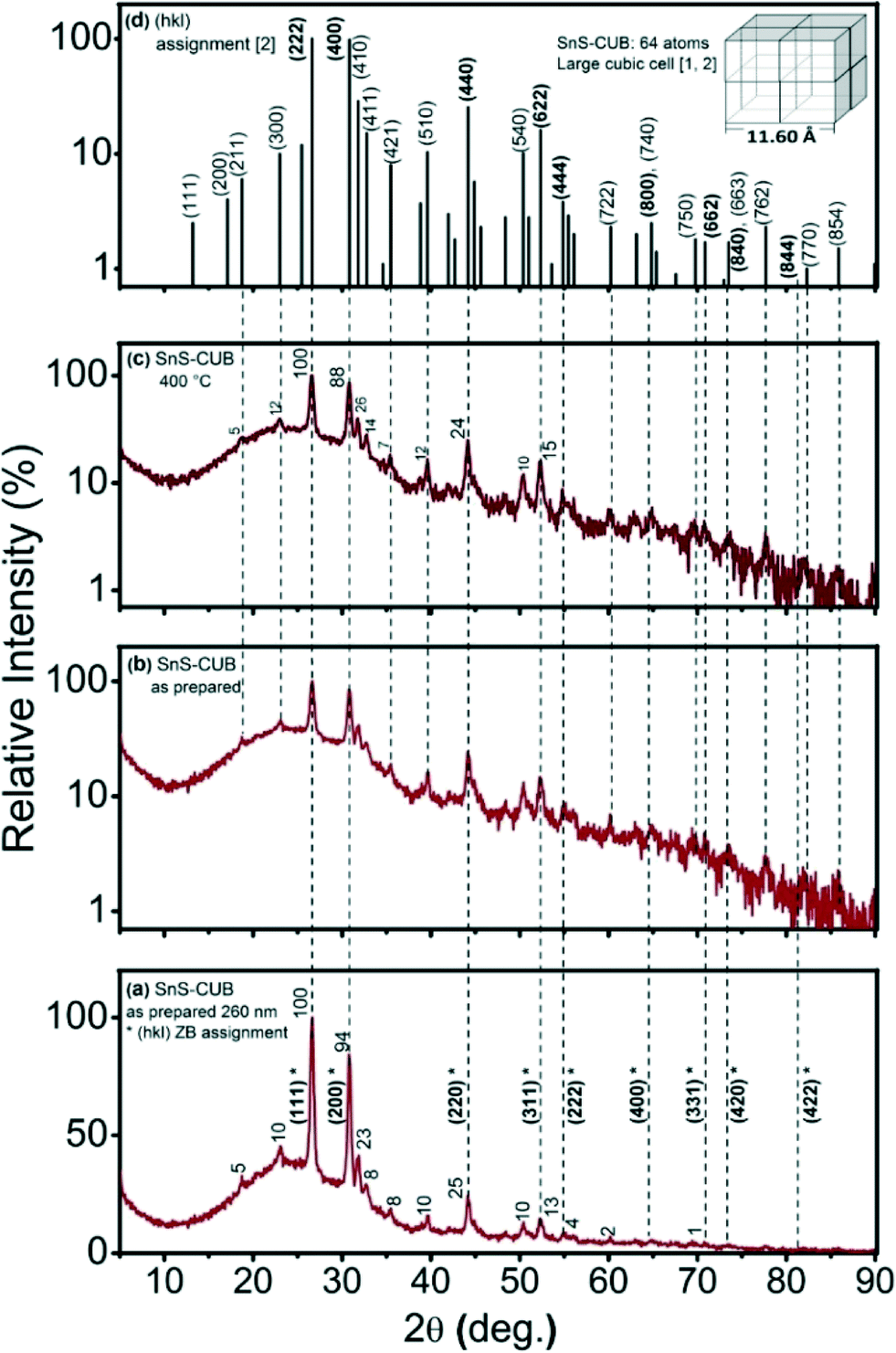 | ||
| Fig. 1 (a) XRD pattern for SnS-CUB thin film of 260 nm in thickness. Relative intensity (numbers) and (hkl)* values as originally assigned assuming a SnS-ZB structure; (b) the same as in (a), but with the intensity data plotted in a logarithmic scale; (c) data recorded for the same film after being heated at 400 °C in a nitrogen atmosphere; (d) assignment of (hkl) indices for a simple cubic unit cell for SnS of a = 11.60 Å. | ||
The ZB structural assignment for SnS-CUB ignored the presence of many diffraction peaks throughout the pattern, of intensities comparable with those of a ZB structure. The triple-peak signature seen in the 30–33° 2θ interval is particularly noteworthy. The 23% intensity of the middle peak is comparable to that of the (220)* peak (25%) assigned to the ZB-structure. This may not be ignored. Also, one should consider that the first among the diffraction peaks for SnS-ORT is the (110) reflection at 2θ = 22.01°, which exhibits a 40% relative intensity (PDF 39-0354).4 The presence of SnS-ORT in SnS-ZB as a minor component could not account for the peaks appearing at 2θ values still lower than those in Fig. 1(a). Furthermore, a plot of Fig. 1(a)'s data, with the intensity on a logarithmic scale provided in Fig. 1(b), reveals many other XRD peaks, more than fifty of these in the 2θ interval of 5–90°. Fig. 1(c) shows that heating the film at 400 °C for 30 min in a nitrogen atmosphere (and subsequent cooling) leaves the XRD pattern nearly unchanged in both 2θ peak positions and relative intensities.
By considering that the XRD patterns in Fig. 1a–c arise from a large simple cube as the basic building block for this thin film, as proposed for the π-SnS nanocrystals,1 the riddle gets solved immediately. All diffraction peaks fit the (hkl) values assigned for a cubic unit cell of a = 11.59–11.60 Å, as shown in the inset in Fig. 1(d). The (hkl) (222), (400), (440), (622), etc., peak positions of this large cube are equivalent to the (111), (200), (220), (311), etc., peak positions of SnS-ZB, as labelled in Fig. 1(a). Detailed analysis of the XRD peak positions obtained for the films places the a-value as follows: “as-prepared” (Fig. 1(a)), 11.59 ± 0.02; “heated at 350 °C” (not shown), 11.59 ± 0.015; and “heated at 400 °C” (Fig. 1(c)), 11.60 ± 0.01 Å. Half this value of a is the same as that known for SnS-RS (5.80 ± 0.02 Å) (PDF 77-3356).5 The thin films consist of crystalline grains of typical 200 Å dimensions (evaluated by using Scherrer's formula, eqn (1)).17 Annealing at 350 °C or 400 °C does not increase the grain diameter. The value of a obtained for the SnS-CUB thin films is in exact coincidence with that for π-SnS nanocrystals (a = 11.595 Å).2 Complete data are given in Table S1 of the ESI.†
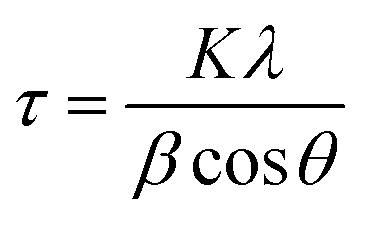 | (1) |
Structural analysis
To account for the relative peak intensities in the diffraction patterns of SnS-CUB, the Sn and S atomic positions must be properly assigned. As an initial step, a cubic unit cell of a = 11.60 Å containing 64 atoms is constructed according to a previous work for π-SnS nanocrystals (a = 11.7 Å, #198 space group (T4 or [P213]).1 The initial step model is modified based on the experimental XRD data to acquire a refined lattice parameter and atomic positions. The refinement procedure was performed using “FULLPROF”18 Rietveld refinement software. The lattice parameter was refined to match the exact experimental peak positions, indicating a unit-cell geometry similar to that of π-SnS. The refined atomic position required only slight changes to match the relative intensities of the XRD diffraction pattern in Fig. 2. Notably, the weighted profile correlation factor (discrepancy index) Rwp = 11.2; any value around 10 and below is considered to represent an excellent fit.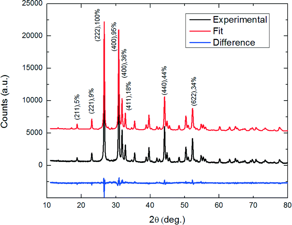 | ||
| Fig. 2 Rietveld refined powder XRD pattern using “FULLPROF” Rwp = 11.2, χ2 = 3.5. Experimental XRD pattern of SnS-CUB phase (black curve), fit XRD pattern for SnS-CUB phase (red curve), and their difference (blue curve). The difference curve indicates a reasonably good match of the fitted crystallographic model to the experimental results. | ||
The XRD patterns of the heated samples are also fully accounted for, with lattice constants differing by less than 0.1%. No additional XRD peaks were observed by heating up to 400 °C. This strengthens the assumption that SnS-CUB thin films establish a stable, phase-pure polymorph of SnS. The experimentally refined atomic positions for Sn and S in the thin films presented here do not differ in any significant manner from those assigned for the π-SnS nanocrystals;1 the difference is less than 2%. This proves that the nanocrystals and the thin films belong to the same crystal structure, thereby validating that SnS-CUB and π-SnS are equivalent. This result is presented in Fig. 3.
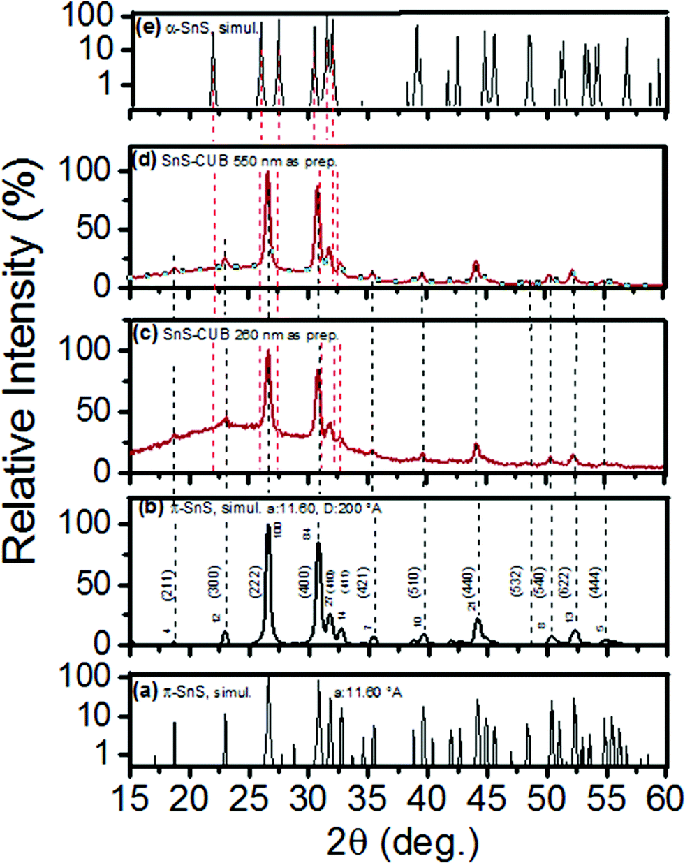 | ||
| Fig. 3 (a) Semi-logarithmic plot of “FULLPROF” software simulated XRD pattern according to a π-SnS crystal1 of lattice constant a = 11.60 Å for a SnS-CUB crystal; (b) simulated powder diffraction pattern for a SnS-CUB film of 200 Å crystalline grain diameter. (hkl) values and relative peak intensities are indicated; (c) and (d) experimental powder diffraction patterns of 260 and 550 nm thick SnS-CUB films, respectively; peak positions are indicated, matching with the simulated (a) and (b) patterns; peak positions are indicated by dashed lines. (e) Simulated XRD pattern of the orthorhombic polymorph of SnS. | ||
Fig. 3(a) shows a semi-logarithmic plot of the simulated intensity versus 2θ pattern for a = 11.60 Å, the same as that for the SnS-CUB thin film in Fig. 1(c). It was obtained in accordance with the earlier report for π-SnS.1 The experimental result of log-scaled intensity versus 2θ pattern in Fig. 1(d) is a good match to this simulated pattern. Fig. 3(b) is the simulated XRD pattern for a crystalline material of SnS-CUB constituted by grains of 200 Å in diameter, representing the thin film heated to 400 °C (Fig. 1c). Here the intensity ratios and 2θ peak positions in Fig. 1(c) are completely replicated upon refinement of the crystallographic parameters (repeated as Fig. 3(c) to aid the comparison). Fig. 3(d) shows the XRD pattern for a SnS-CUB film of 550 nm in thickness, as used in a solar cell structure.7 Again, a complete fit is seen with that of the simulated XRD pattern in Fig. 3(b). Fig. 3(e) is a simulated XRD pattern of the orthorhombic polymorph of SnS, which is entirely distinct from that of Fig. 3(a) for the large cubic π-SnS.
The large cubic tin sulfide polymorph
The atomic positions for Sn and S within the 64-atom unit cell are presented in Fig. 4. All atomic sites are labelled. The Wyckoff sites, site symmetry and multiplicity, and atomic positions are detailed in Table 1.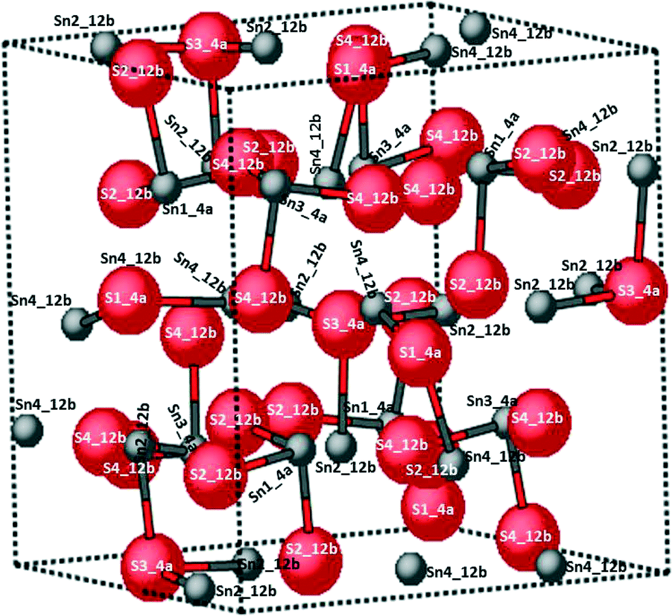 | ||
| Fig. 4 Large simple cubic unit cell with the 64 atoms listed in Table 1. The red and grey atom contours denote sulfur (S) and tin (Sn) ions, respectively. | ||
| Atom name | Wyckoff position | Atomic position | ||||
|---|---|---|---|---|---|---|
| Type | Multiplicity | Symmetry | x/a | y/a | z/a | |
| S1 | a | 4 | C 3 | 0.9540(11) | 0.9540(11) | 0.9540(11) |
| S2 | b | 12 | C 1 | 0.0533(12) | 0.7659(9) | 0.1891(9) |
| S3 | a | 4 | C 3 | 0.5312(13) | 0.5312(13) | 0.5312(13) |
| S4 | b | 12 | C 1 | 0.2576(13) | 0.7984(11) | 0.9514(17) |
| Sn1 | a | 4 | C 3 | 0.7712(2) | 0.7712(2) | 0.7712(2) |
| Sn2 | b | 12 | C 1 | 0.0220(4) | 0.9804(3) | 0.2312(3) |
| Sn3 | a | 4 | C 3 | 0.0224(3) | 0.2224(3) | 0.2224(3) |
| Sn4 | b | 12 | C 1 | 0.0216(4) | 0.7430(2) | 0.9683(3) |
A representation of the well-known SnS-ORT structure is given for comparison in Fig. 5(a) along with a view of the atomic positions in the new cubic unit cell in Fig. 5(b). SnS-ORT exhibits a layered structure: each atom is covalently bonded within the layer, and adjacent layers are bonded by the weaker van der Waals forces.19 Each layer comprises asymmetric pyramidal SnS3 and SSn3 sub-structures shown in Fig. 5(a). The newly discovered cubic structure exhibits a change in these sub-structures: each atom in a “4a” site is connected to three “12b”-sited atoms of the opposite valence with a 3-fold symmetry, creating together highly symmetric pyramidal sub-structures, as illustrated in Fig. 5(c). By a more detailed description, the cubic tin sulfide unit cell exhibits 16 pyramidal sub-structures classified into two pyramidal pair-types.
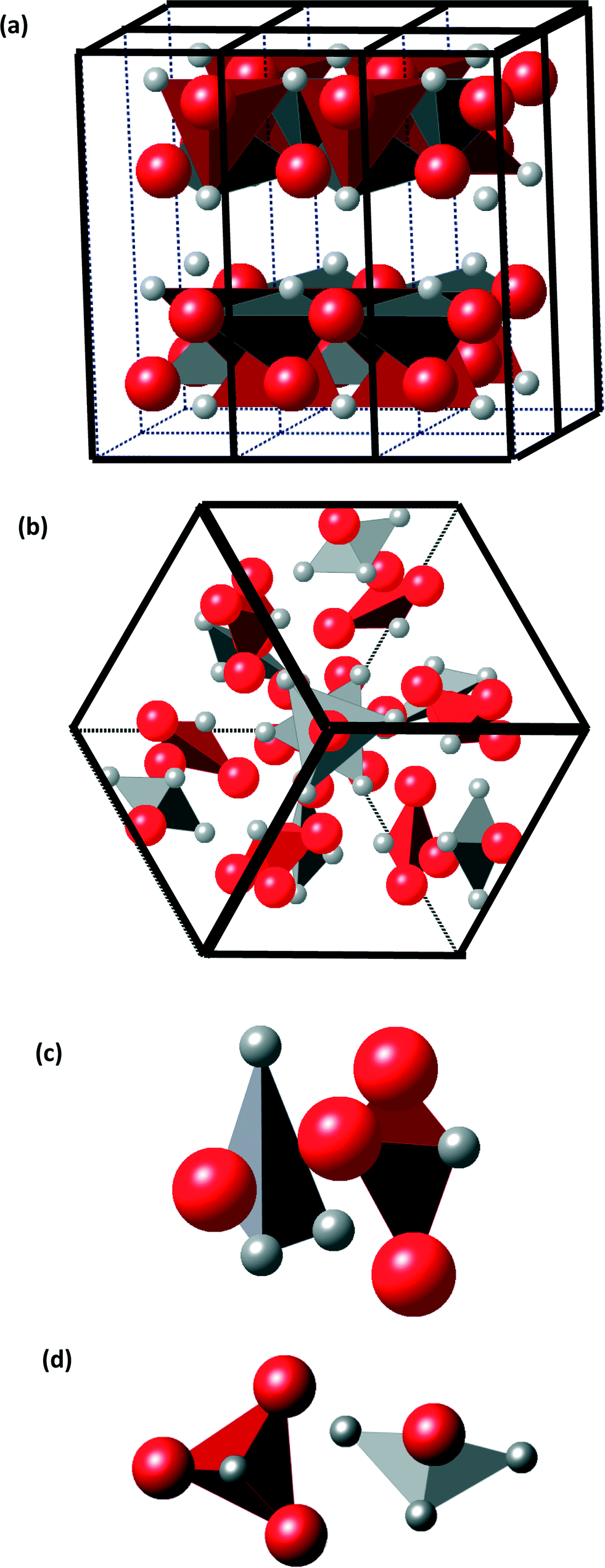 | ||
| Fig. 5 (a) Orthorhombic structure; (b) large cubic tin sulfide structure viewed along the [111] zone axis; (c) first type of bonding: facing-pyramids (only participating atoms are highlighted); (d) second type of bonding: chain-like (only participating atoms are highlighted). | ||
In the first class of pyramidal pairs, a Sn1, 4a-sited tin atom acting as the vertex is bonded to three S2, 12b-sited sulfur atoms. It is paired with an adjacent pyramid comprising a sulfur S3, 4a-sited atom acting as the vertex, bonded to three tin Sn2, 12b-sited atoms. There are 4 such pyramidal pairs. In the second class of pyramidal pairs, a Sn3, 4a-sited tin atom acting as the vertex is bonded to three S4 12b-sited sulfur atoms. It is paired with an adjacent pyramid comprising a sulfur S1, 4a-sited ion acting as the vertex, bonded to three Sn4 tin 12b-sited ions. There are 4 such pyramidal pairs. Assuming some ionicity η to the inter-atomic bonding, the electrical charge on a tin-vertexed pyramid is 4η−; the electrical charge on a sulfur-vertexed pyramid is 4η+.
The relative spatial posture of the oppositely charged pyramids is illustrated in Fig. 5(c) and (d). For the first class of pyramidal pairs, the two oppositely charged pyramids face each other by the bases, which are nearly parallel. These pairs are closely packed, with an inter-pyramidal distance (distance between mass centers) of only 2.6 Å. This is an indication of a strong chemical bonding. For the second class of pyramidal pairs, the bases are nearly perpendicular. The inter-pyramidal distance (distance between mass centers) is approximately 4.6 Å, indicating a weaker bonding. The 21 symmetry element refers to a screw axis present along each of the main crystallographic axes of the cubic cell, <100>. It represents a 2-fold rotation followed by a translation of half of the unit cell. These said second-class pyramidal pairs reside closest to the 21 unit-cell screw axis. The occurrence of the two classes of spatial inter-pyramidal postures suggests that the pairs in each class are bonded through different molecular orbitals. Often, the spatial relative posture of molecules relates to their internal bonding type.
The stability of the SnS-CUB phase is demonstrated by DFT calculations conducted in a previous work,2 which showed that π-SnS is only slightly less stable than the orthorhombic phase. This removes the concern raised earlier for the use of this material in solar cell applications – the thermodynamic instability noted in the DFT studies on SnS-ZB11,12 led to it being side-lined in solar cell structures. The stability of SnS-CUB solar cells has already been demonstrated.7 Its relatively large band gap (1.7 eV) is fully accounted for theoretically2 and the benefit of using combined SnS-ORT/SnS-CUB absorbers for increased current density in solar cells has been suggested.3
Salient features of the π-SnS polymorph
It is worth noting that the #198 (P213) space group of the π -SnS phase is non-centrosymmetric – it lacks a center of symmetry. This leads to some interesting potential behaviour of this material, which we would highlight here. There are 21 non-centrosymmetric crystal classes of which only 20 give rise to piezoelectricity.20 The large cubic crystal of π-SnS is among the materials whose piezoelectric moduli don’t vanish. Other properties originating from the crystal symmetry are optical activity and second harmonic generation (SHG). Being a non-centrosymmetric material is a necessary, but not a sufficient requirement for π-SnS to exhibit these properties. Enantiomorphism is also associated with this space group. Enantiomorphic crystals could be of one-handedness, L or R and can show opposite optical activity behaviour. This means that light waves traveling through the crystal will exhibit an interesting behavior. Linearly polarized light will experience rotation of the plane of polarization. The rotation direction (clockwise or counterclockwise) depends on the enantiomer type present. Light may also interact with the crystal in such a manner that it will produce new waves with frequency twice that of the incident wave. This optical SHG is due to the nonlinear optical susceptibility. While these features might appear in SnS-CUB, they are not expected from the orthorhombic phase of SnS which belongs to a centrosymmetric crystal class #62 D162h (Pnma).19 We hope that the present work would stimulate further investigation into new opportunities arising from the newly discovered π-SnS/SnS-CUB.We further note that the unique atomic arrangement in the large cubic unit cell described above is not limited only to tin monosulfide. Recent publications from our groups reported that a crystalline structure analogous to π-SnS could be found also in the SnSe system. This new polymorph of tin monoselenide has a slightly larger unit cell, a = 11.97 Å, and the atomic positions are similar to those of π-SnS described in Fig. 4. This π-SnSe polymorph was obtained in the form of surfactant coated nanoparticles21 or in the form of solution deposited thin films.22 Due to the similarities in atomic positions and cell geometry, many of the features discussed above for the π-SnS structure should be relevant also for the cubic polymorph π-SnSe.
Conclusions
In this work we have unequivocally assigned the crystalline structure of SnS-CUB obtained by chemical deposition to a large simple cubic structure, similar to that previously assigned to π-SnS nanocrystals,1,2 thereby establishing that these materials are compositionally and structurally equivalent. The lattice constant of this cube is a = 11.59–11.7 Å,1–3 depending on the preparation conditions and characterization technique used. We have described the positions of 64 atoms within this cubic cell, which accounts for the XRD peak positions and relative intensities. This work removes the doubt previously expressed concerning the stability of this material, when it has been assigned the zinc blende structure. The large cubic structure and associated bonding scheme suggest thermal stability for this material. The stability of the cubic phase has been demonstrated both experimentally (this work) and theoretically through DFT.2 This places cubic tin monosulfide as a mainstream photovoltaic material, along with its more common orthorhombic polymorph. Additionally, new and potentially useful physical properties are expected for π-SnS, originating from the large cubic crystal structure which is devoid of centro-symmetry. Such features are likely to find potential use in a variety of applications in addition to their traditional use in energy harvesting.Author contributions
REA (BGU) did the structural simulation work on the thin films. The experimental XRD patterns of the films were obtained and analysed by ARGA. Hence they are equal contributors. ZB assisted REA and participated in very useful discussions, and MTSN initiated SnS-CUB work and advised ARGA. PKN (UNAM) and YG (BGU) planned and coordinated the research and the manuscript writing and are the corresponding authors for the work.Acknowledgements
We are grateful to Patricia Altuzar's XRD measurements (UNAM) and to Oscar Gomez Daza for helping with the laboratory management. Financial support for this work was received from PAPIIT-UNAM IN116015 and IT100814, and from CONACYT-LIFYCS and CeMIE-Sol-35. ARGA acknowledges CONACYT (MEXICO) for a graduate fellowship. We thank Dr. Dmitry Mogilyanski for expert assistance in XRD (BGU). This work was partially supported by the Israel Science Foundation, Grant #156/2014, and by the FTA program of the Israel National Nanotechnology Initiative.References
- A. Rabkin, S. Samuha, R. E. Abutbul, V. Ezersky, L. Meshi and Y. Golan, Nano Lett., 2015, 15(3), 2174–2179 CrossRef CAS PubMed.
- R. E. Abutbul, E. Segev, L. Zeiri, V. Ezersky, G. Makov and Y. Golan, RSC Adv., 2016, 6(7), 5848–5855 RSC.
- P. K. Nair, A. R. Garcia-Angelmo and M. T. S. Nair, Phys. Status Solidi A, 2016, 213(1), 170–177 CrossRef CAS.
- Schnering H. G. and H. Wiedemeier, Z. Kristallogr., 1981, 156(1–2), 143–150 Search PubMed.
- B. F. Bilenkii, A. G. Mikolaichuk and D. M. Freik, Phys. Status Solidi, 1968, 28(1), K5–K7 CrossRef CAS.
- P. Sinsermsuksakul, J. Heo, W. Noh, A. S. Hock and R. G. Gordon, Adv. Energy Mater., 2011, 1(6), 1116–1125 CrossRef CAS.
- A. R. Garcia-Angelmo, R. Romano-Trujillo, J. Campos-Álvarez, O. Gomez-Daza, M. T. S. Nair and P. K. Nair, Phys. Status Solidi A, 2015, 2340(10), 2332–2340 CrossRef.
- E. C. Greyson, J. E. Barton and T. W. Odom, Small, 2006, 2(3), 368–371 CrossRef CAS PubMed.
- D. Avellaneda, G. Delgado, M. T. S. Nair and P. K. Nair, Thin Solid Films, 2007, 515(15), 5771–5776 CrossRef CAS.
- D. Avellaneda, M. T. S. Nair and P. K. Nair, J. Electrochem. Soc., 2008, 155(7), D517 CrossRef CAS.
- M. Ichimura, Sol. Energy Mater. Sol. Cells, 2009, 93(3), 375–378 CrossRef CAS.
- L. A. Burton and A. Walsh, J. Phys. Chem. C, 2012, 116(45), 24262–24267 CAS.
- A. J. Biacchi, D. D. Vaughn and R. E. Schaak, J. Am. Chem. Soc., 2013, 135(31), 11634–11644 CrossRef CAS PubMed.
- C. Gao, H. Shen, L. Sun, H. Huang, L. Lu and H. Cai, Mater. Lett., 2010, 64(20), 2177–2179 CrossRef CAS.
- I. Y. Ahmet, M. S. Hill, A. L. Johnson and L. M. Peter, Chem. Mater., 2015, 27(22), 7680–7688 CrossRef CAS.
- R. J. Traill and R. W. Boyle, Am. Mineral., 1955, 40(7–8), 555–559 CAS.
- A. L. Patterson, Phys. Rev., 1939, 56(10), 978–982 CrossRef CAS.
- J. Rodrigues-Carvajal, Software FULLPROF-98, Version 5.06, 2015 Search PubMed.
- R. E. Rundle and D. H. Olson, Inorg. Chem., 1964, 3(4), 596–598 CrossRef CAS.
- J. Zussman, International Tables for Crystallography. Mineral. Mag., 1986, vol. 50, issue 356, pp. 355–355 Search PubMed.
- R. E. Abutbul, E. Segev, S. Samuha, L. Zeiri, V. Ezersky, G. Makov and Y. Golan, CrystEngComm, 2016, 18(11), 1918–1923 RSC.
- P. K. Nair, E. Barrios-Salgado and M. T. S. Nair, Phys. Status Solidi A, 2016, 1–8, DOI:10.1002/pssa.201533040.
Footnote |
| † Electronic supplementary information (ESI) available: Summary of analyses of the XRD patterns. See DOI: 10.1039/c6ce00647g |
| This journal is © The Royal Society of Chemistry 2016 |