 Open Access Article
Creative Commons Attribution 3.0 Unported Licence
A novel dimethylformamide (DMF) free bar-cast method to deposit organolead perovskite thin films with improved stability†
Eurig W.
Jones
a,
Peter J.
Holliman
*a,
Arthur
Connell
a,
Matthew L.
Davies
b,
Jennifer
Baker
b,
Robert J.
Hobbs
a,
Sanjay
Ghosh
a,
Leo
Furnell
a,
Rosie
Anthony
a and
Cameron
Pleydell-Pearce
b
aSchool of Chemistry, Bangor University, Bangor, Gwynedd LL57 2UW, UK
bSPECIFIC, Swansea University, Swansea, SA1 8EN, UK. E-mail: p.j.holliman@bangor.ac.uk
First published on 24th February 2016
Abstract
We report a solvent-free approach to synthesizing organolead perovskites by using solid state reactions to coat perovskite crystals onto Al2O3 or TiO2 nanoparticles followed by addition of terpineol affording perovskite inks. We have bar cast these inks to produce photoactive perovskite thin films which are significantly more stable to humidity than solution-processed films. This new method also avoids the use of toxic DMF solvent.
Since the initial reports of organolead halide perovskite solar cells,1,2 device efficiencies have risen rapidly towards 20%.3 It has also been demonstrated that such perovskites work efficiently in a variety of PV device architectures4 including planar TiO2 charge collection layers5 and mesoporous TiO2 as well as in batteries6a and sensors.6b Electrically-insulating Al2O3 scaffolds1 and even hole transporter-free perovskite devices7 have been reported, demonstrating that the perovskite absorber layer can efficiently sustain charge transport. This is important because key limiting factors for perovskite solar cells are the surface coverage and crystallisation steps which occur at the perovskite–metal oxide interface during device manufacture. As a result, perovskite device manufacturing is the subject of much interest. A current limitation for one-step, solution processed perovskites is infiltration into the mesoporous scaffold, which can be improved by sequential deposition,8 affording superior coverage and avoiding the need for a perovskite capping layer. However, concerns remain over the solvents used for solution processed perovskites9 and the stability of the resulting materials to temperature and/or moisture.10,11 As such, recent reports suggest optimum fabrication conditions such as %RH < 1%10 which complicates scale up.
To date, the choice of perovskite processing solvent has been limited to dimethylformamide (DMF),1 dimethylsulfoxide (DMSO)12 or γ-butyrolactone (GBL)2 given the need to dissolve the PbX2 precursor (X = Cl, Br, I). By comparison, methyl ammonium halides are readily soluble in most solvents including water. In this paper, we report that a 1![[thin space (1/6-em)]](https://www.rsc.org/images/entities/char_2009.gif) :
:![[thin space (1/6-em)]](https://www.rsc.org/images/entities/char_2009.gif) 1 ratio of PbX2 and CH3NH3X react readily together with quantitative yield in solvent-free, solid state reactions by grinding/milling (ESI,† Fig. S1). We have also studied the addition of metal oxide nanoparticles (Al2O3 or TiO2) as common scaffold materials for perovskite solar cells during or after the solid state perovskite reaction. After perovskite has formed on the metal oxide surface, to produce a printable ink, we have ground the particles in terpineol as a suspending media rather than a solvent. Perovskite crystals have previously been suspended in DMF12 but here terpineol has been chosen because it has low toxicity and is widely used in printing media. It also possesses a high boiling point (219 °C), which is similar to DMSO (189 °C) which has been reported to stabilise solvent–PbI2 complexes and inhibit PbI2 crystallization.13 This also avoids the DMF volatilisation (b.p. 153 °C) during spin coating, which increases perovskite crystal dislocations. Higher boiling solvents also encourage slower perovskite crystal growth during annealing. The resultant inks can then be doctor bladed or bar cast. We have studied the influence of metal oxide loading and found that, for Al2O3, a loading of >10% Al2O3 is required to cast a uniform layer, presumably because Al2O3 acts as a plasticizer. This is more than the 5% Al2O3 reported by Carnie et al.14 for their DMF/perovskite/Al2O3 nanoparticle precursor in their spin coating based study. The difference is that the perovskite particles are pre-formed on the Al2O3 particle surfaces in our inks and no DMF is present unlike previous reports of bar-cast perovskites.15 Visual inspection also suggests that the resulting colloidal inks are stable for >3 months. An additional advantage of developing inks for meso-scopic perovskite solar cells using a passive Al2O3 scaffold is their low-temperature processability. Thus, our inks can be deposited under ambient conditions and heated at 110 °C because high temperature processing is not required to ensure inter-particle “necking” to carry electrical charge as is the case for TiO2 photo-electrodes.16 This is in line with previous reports for Al2O3 where heat processing is shown to be complete at 150 °C17 and 110 °C.14 The perovskite ink formation is described in eqn (1) and (2).
1 ratio of PbX2 and CH3NH3X react readily together with quantitative yield in solvent-free, solid state reactions by grinding/milling (ESI,† Fig. S1). We have also studied the addition of metal oxide nanoparticles (Al2O3 or TiO2) as common scaffold materials for perovskite solar cells during or after the solid state perovskite reaction. After perovskite has formed on the metal oxide surface, to produce a printable ink, we have ground the particles in terpineol as a suspending media rather than a solvent. Perovskite crystals have previously been suspended in DMF12 but here terpineol has been chosen because it has low toxicity and is widely used in printing media. It also possesses a high boiling point (219 °C), which is similar to DMSO (189 °C) which has been reported to stabilise solvent–PbI2 complexes and inhibit PbI2 crystallization.13 This also avoids the DMF volatilisation (b.p. 153 °C) during spin coating, which increases perovskite crystal dislocations. Higher boiling solvents also encourage slower perovskite crystal growth during annealing. The resultant inks can then be doctor bladed or bar cast. We have studied the influence of metal oxide loading and found that, for Al2O3, a loading of >10% Al2O3 is required to cast a uniform layer, presumably because Al2O3 acts as a plasticizer. This is more than the 5% Al2O3 reported by Carnie et al.14 for their DMF/perovskite/Al2O3 nanoparticle precursor in their spin coating based study. The difference is that the perovskite particles are pre-formed on the Al2O3 particle surfaces in our inks and no DMF is present unlike previous reports of bar-cast perovskites.15 Visual inspection also suggests that the resulting colloidal inks are stable for >3 months. An additional advantage of developing inks for meso-scopic perovskite solar cells using a passive Al2O3 scaffold is their low-temperature processability. Thus, our inks can be deposited under ambient conditions and heated at 110 °C because high temperature processing is not required to ensure inter-particle “necking” to carry electrical charge as is the case for TiO2 photo-electrodes.16 This is in line with previous reports for Al2O3 where heat processing is shown to be complete at 150 °C17 and 110 °C.14 The perovskite ink formation is described in eqn (1) and (2).
[PbX2 + Al2O3] + CH3NH3X → [CH3NH3PbX3![[thin space (1/6-em)]](https://www.rsc.org/images/entities/char_2009.gif) : :![[thin space (1/6-em)]](https://www.rsc.org/images/entities/char_2009.gif) Al2O3] Al2O3] | (1) |
[CH3NH3PbX3![[thin space (1/6-em)]](https://www.rsc.org/images/entities/char_2009.gif) : :![[thin space (1/6-em)]](https://www.rsc.org/images/entities/char_2009.gif) Al2O3] + terpineol → Perovskite ink Al2O3] + terpineol → Perovskite ink | (2) |
![[thin space (1/6-em)]](https://www.rsc.org/images/entities/char_2009.gif) :
:![[thin space (1/6-em)]](https://www.rsc.org/images/entities/char_2009.gif) 1 ratio of CH3NH3I
1 ratio of CH3NH3I![[thin space (1/6-em)]](https://www.rsc.org/images/entities/char_2009.gif) :
:![[thin space (1/6-em)]](https://www.rsc.org/images/entities/char_2009.gif) PbCl2 was used along with spin coating to control layer thickness. However, the I
PbCl2 was used along with spin coating to control layer thickness. However, the I![[thin space (1/6-em)]](https://www.rsc.org/images/entities/char_2009.gif) :
:![[thin space (1/6-em)]](https://www.rsc.org/images/entities/char_2009.gif) Cl ratio of the resultant CH3NH3PbI2Cl was reported as 2
Cl ratio of the resultant CH3NH3PbI2Cl was reported as 2![[thin space (1/6-em)]](https://www.rsc.org/images/entities/char_2009.gif) :
:![[thin space (1/6-em)]](https://www.rsc.org/images/entities/char_2009.gif) 1. Effectively, this means that an excess of CH3NH3I is required to convert all the PbCl2 into perovskite. Whilst CH3NH3X waste is less of an issue at the laboratory scale, it is not viable for a scaled process because it multiplies raw material costs and environmental impact which has been reported to be greater for CH3NH3I than for PbX2.18 By comparison, in the solid state reactions, CH3NH3X and PbX2 can be reacted together in the desired ratio and this ratio is carried through into the resulting perovskite material. A further advantage of solid state reactions is much greater control of trace components (e.g. Cl−) which is known to be key to device performance.19
1. Effectively, this means that an excess of CH3NH3I is required to convert all the PbCl2 into perovskite. Whilst CH3NH3X waste is less of an issue at the laboratory scale, it is not viable for a scaled process because it multiplies raw material costs and environmental impact which has been reported to be greater for CH3NH3I than for PbX2.18 By comparison, in the solid state reactions, CH3NH3X and PbX2 can be reacted together in the desired ratio and this ratio is carried through into the resulting perovskite material. A further advantage of solid state reactions is much greater control of trace components (e.g. Cl−) which is known to be key to device performance.19
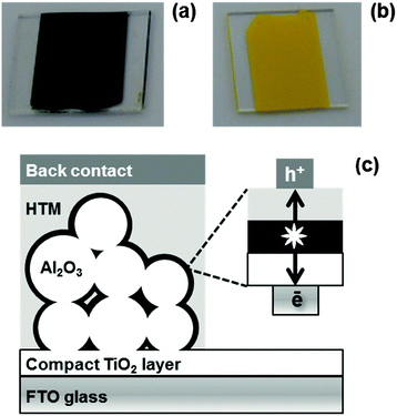
To prepare organolead perovskites on Al2O3, PbX2 (X = Cl, Br, I) and Al2O3 nanoparticles (mean size 13 nm) are ground together until there is no further colour change. After adding the desired CH3NH3X to this the mixture is ground together again. Conversion to a perovskite phase varies depending on the halides used. For CH3NH3PbI3−xClx, an intermediate non-perovskite yellow phase is obtained (Fig. 1b) which only turns black and converts to perovskite after heating at 120 °C for 50 min (i.e. standard solution processing conditions). A similar intermediate perovskite complex, has been previously reported by Wu et al.13 By comparison, the CH3NH3PbI3 ink turns black purely by mechanical mixing and before heating at 120 °C (Fig. 1a). We have defined the pre-heated tri-iodide as “semi-perovskite” ink as the XRD data confirm significant amounts of unconverted PbI2 are still present, which then decrease after heating. Finally, CH3NH3PbBr3 turns orange on grinding which fully converts and increases in crystallinity on heating (ESI,† Fig. S3). Upon the addition of terpineol, each reaction continues to completion and we believe the terpineol assists in a wet grinding process whereby the size of the PbX2 and CH3NH3X crystals are further reduced and these particles are more intimately mixed enabling intercalation of CH3NH3X into the lead halide lattice to form crystalline perovskite.
 | ||
| Fig. 1 (a) Semi-perovskite, (b) perovskite intermediate and (c) schematic of perovskite device architecture. | ||
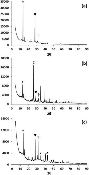
X-Ray powder diffraction data show that the solid state reaction between CH3NH3I and PbI2 produces predominantly the CH3NH3PbI3 phase with only low intensity peaks observed for PbI2 (Fig. 2b). Unconverted PbI2 has been reported previously in the two-step solution processing method, even when the substrate is heated to 60 °C, to constrain lateral crystal growth.20 The PbI2 peaks observed in our work (ground samples) more closely resemble data observed for samples deposited on optimally pre-heated (50 °C) substrates, which is typically done to assist small particle formation and improve coverage.13 After grinding in terpineol (Fig. 2c), the (110) peak for the perovskite phase increases in relative intensity, confirming that the solid state reaction continues on further grinding in the solvent. Data from line broadening suggest that the average crystal/domain size is ca. 100 nm which is similar to that typically observed purely for one-step solution processing methods rather than the larger 500 nm particle sizes observed using the two-step method.17 In addition for both ground samples, there is less evidence of preferred orientation (Fig. 2b and c) compared to solution deposited material (Fig. 2a). This is to be expected as the solution deposited samples nucleate and grow directly onto a flat substrate which is heated from below making perpendicular crystal growth much more likely. By comparison, the ground samples nucleate and crystallise onto randomly oriented metal oxide particles so the orientation of their crystal growth will also be randomised.
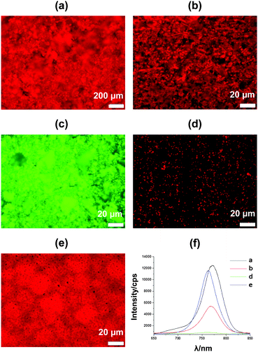
Photoluminescence (PL) of perovskite films is strongly linked to device efficiency21 and so PL microscopy and in situ spectroscopy of perovskite:metal oxide films was carried out to evaluate surface coverage and electron shuttling. The data show that films of doctor bladed CH3NH3PbI3−xClx, bar cast CH3NH3PbI3−xClx and CH3NH3PbBr3 are all emissive, which suggests they should all be photo-active in PV devices (Fig. 3a–c). As expected, the thicker 7 μm doctor bladed CH3NH3PbI3−xClx film (Fig. 3a and f) shows PL intensity which is much greater than that of the equivalent 400 nm bar cast film (Fig. 3b and f). Interestingly, the intensity of the doctor bladed film is comparable to the solution processed image (Fig. 3e and f). In terms of coverage, two issues need consideration. Firstly, there is the coverage of the mesoporous Al2O3 film on the substrate and secondly there is the coverage of the perovskite layer on the Al2O3 surface. For the doctor bladed film, the perovskite coverage on the Al2O3 surface appears to be consistent whilst the mesoporous Al2O3 film is much less even. However, there do not appear to be any pin holes in this film which would cause short circuiting in PV devices made from this material. By comparison, the coverage of the perovskite on the Al2O3 surface in the bar coated film appears less complete although the mesoporous Al2O3 film itself still appears to be complete. For the analogous bar coated CH3NH3PbBr3 sample, greater PL intensity is observed than for the CH3NH3PbI3−xClx sample although at λ ca. 540 nm reflecting the larger band gap for the tribromide perovskite. Here, the perovskite coverage on Al2O3 seems fairly complete although some areas seem brighter than others suggesting variable particle sizes of perovskite crystals have been deposited (Fig. 3c). To further study scaffold coverage, a TiO2-based CH3NH3PbI3 paste was bar coated onto a glass substrate. The maximum PL intensity for this sample is ca. 600 cps compared to ca. 12![[thin space (1/6-em)]](https://www.rsc.org/images/entities/char_2009.gif) 000 cps for the doctor bladed and ca. 6000 cps bar coated CH3NH3PbI3−xClx films. Firstly, this suggests that the perovskite films formed can effectively inject into an electrically-conducting scaffold whilst the PL mapping (Fig. 3d) of TiO2-based perovskite ink shows areas of low PL intensity across the film surface. As the films are not under load, we expect emission to be faster than injection so the low emission for this film may reflect poor coverage or lower stability of the CH3NH3PbI3 on TiO2. By comparison, the more uniform emission across the perovskite:Al2O3 films confirms better coverage and perovskite stability and could also suggest lower losses at grain boundaries or crystal interfaces where emission might be quenched. Ultimately, assuming that more emission relates to more potential charge extraction in a PV device under load and given the need for PV devices to possess lifetimes of many years this suggests Al2O3 scaffolds should be preferable to TiO2. Furthermore, perovskites which have been solution processed onto metal oxide scaffolds exhibit slightly blue-shifted emission (760 nm vs. 750 nm) as a result of confined growth within mesoporous films.22,23Fig. 3f shows that the PL peaks of the ink-based films are similarly blue shifted compared to the solution processed film. This suggests that the perovskite crystals from perovskite inks are similar in size to those grown inside scaffolds, using standard solution processed methods (i.e. typically <100 nm). Perovskite film morphology has also been investigated by SEM (ESI,† Fig. S5–S8) which shows the best perovskite coverage for CH3NH3PbBr3 ink in line with the higher intensity PL data for this film.
000 cps for the doctor bladed and ca. 6000 cps bar coated CH3NH3PbI3−xClx films. Firstly, this suggests that the perovskite films formed can effectively inject into an electrically-conducting scaffold whilst the PL mapping (Fig. 3d) of TiO2-based perovskite ink shows areas of low PL intensity across the film surface. As the films are not under load, we expect emission to be faster than injection so the low emission for this film may reflect poor coverage or lower stability of the CH3NH3PbI3 on TiO2. By comparison, the more uniform emission across the perovskite:Al2O3 films confirms better coverage and perovskite stability and could also suggest lower losses at grain boundaries or crystal interfaces where emission might be quenched. Ultimately, assuming that more emission relates to more potential charge extraction in a PV device under load and given the need for PV devices to possess lifetimes of many years this suggests Al2O3 scaffolds should be preferable to TiO2. Furthermore, perovskites which have been solution processed onto metal oxide scaffolds exhibit slightly blue-shifted emission (760 nm vs. 750 nm) as a result of confined growth within mesoporous films.22,23Fig. 3f shows that the PL peaks of the ink-based films are similarly blue shifted compared to the solution processed film. This suggests that the perovskite crystals from perovskite inks are similar in size to those grown inside scaffolds, using standard solution processed methods (i.e. typically <100 nm). Perovskite film morphology has also been investigated by SEM (ESI,† Fig. S5–S8) which shows the best perovskite coverage for CH3NH3PbBr3 ink in line with the higher intensity PL data for this film.
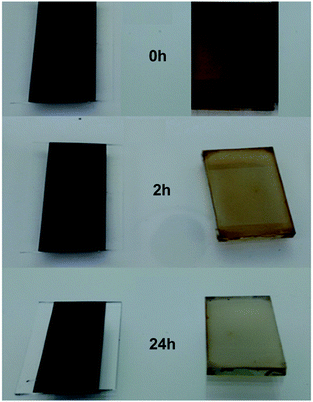
The lifetime of the perovskite films has also been studied (Fig. 4). The data show that Al2O3-based films exhibit significantly better resistance to atmospheric exposure (air, humidity, light) than solution processed films. We have observed that the first stage of humidity-driven perovskite degradation involves phase separation into PbX2 and CH3NH3X but that both materials remain on the surface. Hence, in the early stages of degradation, the process can be reversed by heating at 100 °C. However, this reversibility is only possible when the PbX2 and CH3NH3X are proximally located on the surface. As further phase separation occurs with time, this process becomes irreversible by heating. However, it can be reversed by drying, grinding and heating to re-mix the PbX2 + CH3NH3X. Here, we believe that the stabilising influence of the Al2O3 is to slow the rate of phase separation and, in doing so, effectively to shift the equilibrium (PbX2 + CH3NH3X ↔ CH3NH3PbX3) towards perovskite. Interestingly, Al2O3 capping layers on the perovskite absorber layer have also been reported as moisture barriers.10 TGA data (ESI,† Fig. S11 and S12) suggest that some terpineol may remain after heating but that this reduces with increasing temperature and/or time. If terpineol acts as a solvent of crystallization it should slow H2O ingress but residual solvent is not expected to limit PV efficiency as it has been reported that small amounts of inert media (e.g. PEG24) do not limit device performance. However, removing all terpineol does not reduce film lifetime (ESI,† Fig. S12) suggesting surface perovskite:Al2O3 interactions may enhance film stability.
 | ||
| Fig. 4 (left) Bar-cast CH3NH3PbI3:Al2O3 perovskite ink and (right) spin coated, solution processed CH3NH3PbI3 films vs. time. | ||
In summary, we have demonstrated that photo-active, organolead perovskites can be prepared by solid state reactions onto Al2O3 scaffolds producing materials with enhanced stability. Whilst this resolves key processing limitations by negating the need for toxic or hygroscopic solvents such as DMF, GBL or DMSO,9 this approach also makes the synthesis of other (e.g. lead-free) organometallic perovskites much simpler as it avoids complex solvent engineering issues25 or complex solvent–solvent extraction techniques.26 In addition, using solid state reactions means that all the raw materials end up in the product which makes it easier to add trace components. Also the printing of pre-made perovskite inks is easily scalable whilst solution-based spin coating is not and the vast majority of precursor solutions are spun away making compositional control very difficult.
References
- M. M. Lee, J. Teuscher, T. Miyasaka, T. N. Murakami and H. J. Snaith, Science, 2012, 338, 643 CrossRef CAS PubMed.
- L. Etgar, P. Gao, Z. Xue, Q. Peng, A. K. Chandriran, B. Liu, M. K. Nazeeruddin and M. Grätzel, J. Am. Chem. Soc., 2012, 134, 17396 CrossRef CAS PubMed.
- W. S. Yang, J. H. Noh, N. J. Jeon, Y. C. Kim, S. Ryu, J. Seo and S. I. Seok, Science, 2015, 348, 1234 CrossRef CAS PubMed.
- T. Salim, S. Sun, Y. Abe, A. Krishna, A. C. Grimsdale and Y. M. Lam, J. Mater. Chem. A, 2015, 3, 8943 RSC.
- M. Liu, M. B. Johnson and H. J. Snaith, Nature, 2013, 501, 395 CrossRef CAS PubMed.
- (a) H.-R. Xia, W.-T. Sun and L.-M. Peng, Chem. Commun., 2015, 51, 13787 RSC; (b) C. Muthu, S. R. Nagamma and V. C. Nair, RSC Adv., 2014, 4, 55908 RSC.
- Y. Jin and G. Chumanov, ACS Appl. Mater. Interfaces, 2015, 7, 12015 Search PubMed.
- N. Yantara, D. Sabba, F. Yanan, J. M. Kadro, T. Moehl, P. P. Boix, S. Mhaisalkar, M. Grätzel and C. Grätzel, Chem. Commun., 2015, 51, 4603 RSC.
- P. J. Holliman, A. Connell, E. W. Jones, S. Ghosh, L. Furnell and R. J. Hobbs, Mater. Res. Innovations, 2016, 19, 508 CrossRef.
- J. Burschka, N. Pellet, S. J. Moon, R. Humphry-Baker, P. Gao, M. K. Nazeeruddin and M. Grätzel, Nature, 2013, 499, 316 CrossRef CAS PubMed.
- S. Luo and W. A. Daoud, J. Mater. Chem. A, 2015, 3, 8992 RSC.
- L. C. Schmidt, A. Pertega, S. Gonzalez-Carrero, O. Malinkiewicz, S. Agouram, G. M. Espallargas, H. J. Bolink, R. E. Galian and J. Perez-Prieto, J. Am. Chem. Soc., 2014, 136, 850 CrossRef CAS PubMed.
- Y. Wu, A. Islam, X. Yang, C. Qin, J. Liu, K. Zhang, W. Peng and L. Han, Energy Environ. Sci., 2014, 7, 2934 Search PubMed.
- M. J. Carnie, C. Charbonneau, M. L. Davies, J. Troughton, T. M. Watson, K. Wojciechowski, H. Snaith and D. A. Worsley, Chem. Commun., 2013, 49, 7893 RSC.
- Y. Deng, E. Peng, Y. Shao, Z. Xiao, Q. Dong and J. Huang, Energy Environ. Sci., 2015, 8, 1544 Search PubMed.
- P. J. Holliman, D. K. Muslem, E. W. Jones, A. Connell, M. L. Davies, C. Charbonneau, M. J. Carnie and D. A. Worsley, J. Mater. Chem. A, 2014, 2(29), 11134 RSC.
- J. M. Ball, M. M. Lee, A. Hey and H. J. Snaith, Energy Environ. Sci., 2013, 6, 1739 Search PubMed.
- N. Espinosa, L. Serrano-Luján, A. Urbino and F. C. Krebs, Sol. Energy Mater. Sol. Cells, 2015, 137, 303 CrossRef CAS.
- Q. Chen, H. Zhou, Y. Fang, A. Z. Stieg, T.-B. Song, H.-H. Wang, X. Xu, Y. Liu, S. Lu, J. You, P. Sun, J. McKay, M. S. Goorsky and Y. Yang, Nat. Commun., 2015, 6, 7269 CrossRef CAS PubMed.
- H.-S. Ko, J.-W. Lee and N.-G. Park, J. Mater. Chem. A, 2015, 3, 8808 RSC.
- F. Deschler, M. Price, S. Pathak, L. E. Klintberg, D.-D. Jarausch, R. Higler, S. Hüttner, T. Leitjens, S. D. Stranks, H. J. Snaith, M. Atatüre, R. T. Phillips and R. H. Friendm, J. Phys. Chem. Lett., 2014, 5, 1421 CrossRef CAS PubMed.
- M. De Bastiani, V. D'Innocenzo, S. D. Stranks, H. J. Snaith and A. Petrozza, APL Mater., 2014, 2, 081509 CrossRef.
- V. D'Innocenzo, G. Grancini, M. J. P. Alcocer, A. R. S. Kandada, S. D. Stranks, M. M. Lee, G. Lanzani, H. J. Snaith and A. Petrozza, Nat. Commun., 2014, 5, 3586 Search PubMed.
- C.-Y. Chang, C.-Y. Chu, Y.-C. Huang, S.-Y. Chang, C.-A. Chen, C.-Y. Chao and W.-F. Su, ACS Appl. Mater. Interfaces, 2015, 7, 4955 Search PubMed.
- N.-J. Jeon, J.-H. Noh, Y.-C. Kim, W.-S. Yang, S. Ryu and S.-I. Seok, Nat. Mater., 2014, 13, 897 CrossRef CAS PubMed.
- Y. Zhou, M. Yang, W. Wu, A. L. Vasiliev, K. Zhu and N. P. Padture, J. Mater. Chem. A, 2015, 3, 8179 Search PubMed.
Footnote |
| † Electronic supplementary information (ESI) available. See DOI: 10.1039/c5cc09859a |
| This journal is © The Royal Society of Chemistry 2016 |


