
 Open Access Article
 This Open Access Article is licensed under a
 Creative Commons Attribution 3.0 Unported Licence
Tunable nanoscale structural disorder in Aurivillius phase, n = 3 Bi4Ti3O12 thin films and their role in the transformation to n = 4, Bi5Ti3FeO15 phase
Nitin
Deepak
*ab,
Patrick
Carolan
a,
Lynette
Keeney
a,
Martyn E.
Pemble
ab and
Roger W.
Whatmore
*abc
aTyndall National Institute, University College Cork, ‘Lee Maltings’, Dyke Parade, Cork, Ireland. E-mail: nitindeepak114@gmail.com
bDepartment of Chemistry, University College Cork, Cork, Ireland
cDepartment of Materials, Faculty of Engineering, Imperial College London, London SW7 2AZ, UK
First published on 5th May 2015
Abstract
Naturally super-latticed Aurivillius phase ferroelectrics can accommodate various magnetic ions, opening up the possibility of making new room temperature multiferroics. Here, we studied the growth of single-phase Aurivillius phase Bi5Ti3FeO15 (BTFO) thin films, grown onto single crystalline SrTiO3 (STO) substrates, by doping Bi4Ti3O12 (BTO) with iron by liquid injection metal–organic chemical vapour deposition. The crystalline properties of the resulting films were characterized by X-ray diffraction and transmission electron microscopy. It has been found that the structural properties of the films depend strongly on the relative iron and titanium precursor injection volumes. Nanoscale structural disorder starts to occur in BTO films on the onset of iron precursor flow. A small iron precursor flow causes the formation of half-unit cells of BTFO inside BTO lattice, which in turns causes disorder in BTO films. This disorder can be tuned by varying iron content in the film. Atomic force microscopy shows how the growth mode switches from island growth to layer-by-layer growth mode as the composition changes from BTO to BTFO.
1. Introduction
Single phase magnetoelectric multiferroic materials that simultaneously possess ferroelectric and ferromagnetic ordering are highly desirable due to their ability to convert an electric response into a magnetic response or vice versa, and for the possibility of coupled magnetic and ferroelectric order parameters. These multiferroic materials have many interesting applications which include four-state logic memories,1 tunnel junctions,2 actuators,3 magnetic field sensors,4 and new types of memory devices where data can be written electrically and read magnetically.5 In order to achieve multiferroicity in single phase materials, various complex systems were studied extensively in the 1950's to 1970's.6–8 The lack of reliable and reproducible materials growth methods combined with the complex nature of these material systems shifted the interests of the research community away from multiferroics.6,8,9 The renaissance of research on multiferroic materials experienced over the last two decades has been driven by the development of better characterization and sample preparation methods while the discovery of ferroelectric and antiferromagnetic behavior in BiFeO3 films by Wang et al.10 gave impetus to research into the use of these thin films for next generation multiferroic devices.The number of single-phase materials demonstrating multiferroic behavior at room-temperature is very small. This is due to the severe electronic structure conditions required for the coexistence of ferroelectricity and ferromagnetism.8 One of the approaches to obtaining magnetoelectric behavior is to use composites, where a magnetostrictive material (e.g. NiFe2O4,11 or alloys, e.g. TbDyFe2 (Terfenol-D)12,13) is bonded to a piezoelectric material with a high piezoelectric coefficient such as Pb(Zr,Ti)O34,14,15 or Pb(Mg1/3Nb2/3)O3–PbTiO3 single crystals16 in order to achieve stress-mediated magnetoelectric coupling between the two different materials. Epitaxial CoFe2O4–BaTiO317 nanocomposites have also been employed in this way. While such composite materials are not true single phase multiferroics, the presence of broken symmetries at the interfaces between oxide films and substrates have been extensively studied in terms of induced multiferroic properties.18,19 Nevertheless, the achievement of multiferroicity at room-temperature in a single phase material remained elusive until recently when the presence of both ferroelectricity and ferromagnetism was demonstrated in Bi6Ti2.8Fe1.52Mn0.68O18 (BTFMO) thin films.20
This material belongs to naturally super-latticed Aurivillius phase perovskite family of materials having general formula (Bi2O2)(An+1BnO3n+1).21,22 ‘n’ in the above formula represents the number of perovskite layers interleaved between two bismuth oxide layers. The properties of the members of this family can be varied by adjusting the value of ‘n’ or by substituting various ions at ‘A’ or ‘B’ sites. Most Aurivillius phase compounds are ferroelectric in nature and magnetic ions can be easily inserted into their flexible structure. Various compounds of Bi4Ti3O12–BiFeO3 (BIT–BFO) series such as Bi5Ti3FeO15, Bi6Ti3Fe2O18 and Bi7Ti3Fe3O21 have been studied for their possible multiferroic behavior due to the presence of BiFeO3 perovskite units.23 Ferromagnetic behavior has been reported in the members of BIT–BFO series, both pure or doped with Co3+, Mn3+ and Nd3+ ions.24–28 However, great care is required while interpreting the ferromagnetic signal as the presence of very small percentages of second-phase impurities, which are hard to detect by conventional microstructural analyses using XRD and SEM (<3%), can potentially account for a substantial proportion (or even the whole) of the detected magnetic signature.29 Careful microstructural analysis is required to ensure that this is not the case.30
Chemical solution deposition (CSD) is a relatively simple, cheap, and versatile method for the growth of complex mixed-valence oxides and for exploring different compositions rapidly. Other methods such as pulsed laser deposition (PLD),31 molecular beam epitaxy (MBE),32 atomic layer deposition (ALD),33 and chemical vapour deposition (CVD)34 have been used to grow epitaxial complex oxide thin films. In the present study a type of CVD known as atomic vapour deposition (AVD)35 (also called liquid injection metal–organic vapour deposition), was used to prepare thin films. The Aurivillius phase system is prone to nanoscale structural disorder due to its complex lattice structure.36 Studying the effect of each component of the film can give clues about the nature of the disorder, and the accuracy of AVD's liquid precursor injection system provides an excellent way of studying the link between film stoichiometry and these defects. Previous studies have shown that similar defects occur unintentionally in these systems due to loss of bismuth, which is volatile at film growth temperatures or excess titanium in Aurivillius phase systems. In this report, it has been shown for the first time that nanoscale defects can be artificially induced in Bi4Ti3O12 structure. A detailed structural analysis was also performed using XRD and TEM in order to understand the transformation mechanism from BTO (n = 3) to BTFO (n = 4) in highly c-axis oriented thin films resulting from induced disorder.
2. Experimental
An Aixtron AIX 200/FE atomic vapour deposition™ (AVD)35 system equipped with a horizontal flow reactor, was used to prepare Bi5Ti3FeO15 (BTFO) thin films on (001) oriented single crystalline SrTiO3 (STO) substrates. STO substrates were cleaned with acetone and isopropyl alcohol prior to deposition. The AVD system is equipped with a liquid precursor delivery system, which carries precursors from stainless-steel bottles to a vaporizer kept at a temperature of 220 °C. Liquid precursors were injected into vaporizer with the help of injectors and the flow of precursors was controlled by changing the number of pulses and temporal width of each pulse. A typical pulse frequency of 1 Hz was used for injection. Bi(thd)3 (thd = 2,2,6,6-tetramethyl-3,5-heptanedionate), Ti(O-iPr)2(thd)2 (where O-iPr = iso-propoxide) and Fe(thd)3 dissolved in dry toluene (final concentration 0.1 M), were used as liquid oxide precursors. 1![[thin space (1/6-em)]](https://www.rsc.org/images/entities/char_2009.gif) :3 ratios of pure oxygen and nitrogen were used as oxidizing agent and carrier gases respectively. Heated lines, kept at a temperature of 220 °C to prevent precursor vapour condensation, were used to carry precursor vapours from vaporizer to the reactor. The susceptor that holds the substrate was heated by IR lamps and the growth temperature was kept constant at 700 °C. No post deposition annealing was performed on the samples. Sample stage was rotated with nitrogen flow at 60 rpm to improve the uniformity of the films. The flow of precursors was monitored using liquid flow meters. The precursor injection sequence can be changed to inject precursors individually or collectively, as per the growth requirements. The injection sequence used for the present study is shown in Fig. 1.
:3 ratios of pure oxygen and nitrogen were used as oxidizing agent and carrier gases respectively. Heated lines, kept at a temperature of 220 °C to prevent precursor vapour condensation, were used to carry precursor vapours from vaporizer to the reactor. The susceptor that holds the substrate was heated by IR lamps and the growth temperature was kept constant at 700 °C. No post deposition annealing was performed on the samples. Sample stage was rotated with nitrogen flow at 60 rpm to improve the uniformity of the films. The flow of precursors was monitored using liquid flow meters. The precursor injection sequence can be changed to inject precursors individually or collectively, as per the growth requirements. The injection sequence used for the present study is shown in Fig. 1.
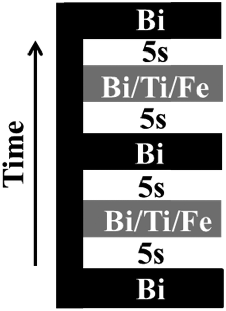 | ||
| Fig. 1 The precursor injection sequence used for growth of BTFO thin films. The iron precursor flow rate is varied while keeping bismuth and titanium precursor flow rates constant. | ||
A time interval of 5 s was used between each set of pulses. Thickness of the film was controlled by repeating this sequence a number of times to get the desired thickness. The flow of the precursors could be controlled with microliter precision to insert monolayers of titanium oxide and iron oxide by varying the opening time and number of pulses injected. This control provides the opportunity to study the effect of very tiny variations of the amounts of precursors on the structural properties. The mechanisms involving the growth of n = 3 (BTO) to n = 4 (BTFO) Aurivillius compounds can thus be easily studied by exploiting the precision of the injector system. This is the first report on the insight of the mechanisms involving transformation from BTO to BTFO systems and role of iron flow rates on their crystalline properties. All the films were characterized using a Panalytical MRD X-ray diffraction (XRD) system for their crystalline properties with filtered Cu Kα radiation. A JOEL 2100 transmission electron microscope (TEM) was used at 200 KV for high resolution cross-sectional imaging of the films. TEM samples were prepared with an FEI quanta focused ion beam (FIB) system. The surface morphology of the films was analysed by Asylum research MFP-3D™ atomic force microscope in AC mode.
3. Results and discussion
To prepare the BTFO thin films, the flow of precursors was varied to achieve the right stoichiometry. The flow of bismuth and titanium precursors was kept constant and iron flow was varied from no iron injection to the flow required for insertion of one full BiFeO3 perovskite unit. The amount of bismuth was kept higher than the required stoichiometry due to the volatile nature of bismuth, and inefficiency of bismuth precursor used.37 All results presented are discussed in terms of Ti/Fe ratio under conditions where the Bi flow was kept constant.The XRD plots in Fig. 2 show the presence of various crystalline phases which are observed after growth using the particular flow rates of iron precursor stated.
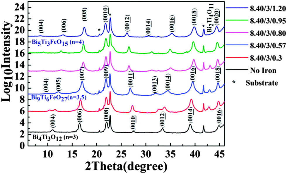 | ||
| Fig. 2 The XRD plots showing the effect of iron precursor flow rate on growth of BTFO thin films from no iron injection at all to the insertion of one full perovskite unit of BiFeO3. Note that all XRD plots are drawn on logarithmic scale to highlight low-intensity peaks and an offset was used between each plot to make them clearly visible. | ||
All peaks are labelled according to the crystal structures and index ‘n’ of Aurivillius phase present at particular iron injection volumes. All XRD plots are drawn on a logarithmic scale to highlight the low intensity peaks which may be evidence for any possible impurity phases. An offset is used for this graph to make individual plots visible clearly. The films are highly c-axis oriented as can be detected from XRD plot shown in Fig. 2. No bismuth oxide impurity phases were observed, even at higher bismuth precursor flow rates. This can be attributed to volatile nature of bismuth and the presence of bismuth self-limiting behavior film growth.35 Starting with no iron flow, the films grow in pure n = 3 BTO phase. Thickness fringes can be observed around the (006) peak confirming the excellent crystalline quality of BTO film. An introduction of iron precursor (Ti/Fe ratio 3/0.3) during the film growth, leads to interesting features in XRD plot. The (004) and (00![[1 with combining low line]](https://www.rsc.org/images/entities/char_0031_0332.gif)
![[2 with combining low line]](https://www.rsc.org/images/entities/char_0032_0332.gif) ) peak of the BTO structure start to split. The data analysis suggests that this splitting arises from the appearance of out-of-phase boundaries (OPB's) in BTO system. Our previous report on BTO thin film system shows that this kind of peak splitting can be caused by the inclusion of an amount of titanium that is in excess of that required for monolayer growth.35 The extra titanium in BTO system causes the OPB defects to form. These occur more often in layer-by-layer growth mode, where a change in local stoichiometry leads to a change in the local crystalline structure and hence gives rise to these defects, which in turn leads to peak splitting observed.
) peak of the BTO structure start to split. The data analysis suggests that this splitting arises from the appearance of out-of-phase boundaries (OPB's) in BTO system. Our previous report on BTO thin film system shows that this kind of peak splitting can be caused by the inclusion of an amount of titanium that is in excess of that required for monolayer growth.35 The extra titanium in BTO system causes the OPB defects to form. These occur more often in layer-by-layer growth mode, where a change in local stoichiometry leads to a change in the local crystalline structure and hence gives rise to these defects, which in turn leads to peak splitting observed.
However, in the present case, the OPB's appear on introducing a small amount of iron in the system during film growth. The BTO thin films (Fig. 2) show no peak splitting. This means that the splitting in the case of iron doped BTO films is not due to titanium excess but to local structural disorder that occurs due to the presence of iron in the structure. The appearance of the peak splitting is also accompanied by a weak impurity peak occurring at 2theta 42.84°, which belongs to a bismuth–titanium phase with chemical composition of Bi2Ti4O11 (B2T4O) and (−406) orientation.
Fig. 3 shows a high resolution cross-sectional TEM image of a BTO thin film prepared by doping with iron (Ti/Fe ratio 3/0.3). The OPB's can be clearly observed in this film. The OPB's shown in these iron doped BTO thin films are different from our previous results on BTO system where they are associated with an excess of Ti4+ ions create them.35 A closer look at the TEM image shown in Fig. 3, of BTO film with Fe3+ impurities reveals the origin of OPB's in this system. The lines highlighted with red and white colours correspond to OPB's and bismuth oxide layers respectively. The regions shown in rectangular yellow and blue boxes highlight the perovskite blocks with the height of half unit cells of BTO and BTFO respectively. An important thing to note in this image is that these BTFO regions are present near the OPB lines. The cause of these half BTFO unit-cells is the presence of Fe3+ ions in the system. There is a charge difference between Fe3+ and Ti4+ ions and the only way to accommodate these Fe3+ ions into the BTO system is the formation of half-unit cells of BTFO to attain the charge neutrality. The amount of iron precursor employed during the film growth is not enough to form n = 3.5 or 4 Aurivillius structure, which engenders the formation of BTFO half-unit cells in patches. The BTFO system consists of one more perovskite unit-cell of BiFeO3 as compared to BTO and so the OPB's tend to nucleate at the BTFO intergrowth sites due to the resulting difference in the c-axis length of BTO and BTFO unit-cells.
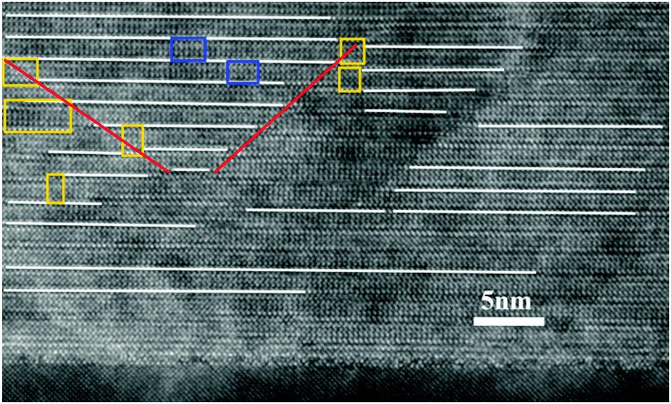 | ||
| Fig. 3 The high resolution TEM image of BTO film with Ti/Fe ratio 3/0.3. OPB's can be clearly observed in this image. | ||
Fig. 4 shows how the presence of half unit cell may change the structure around it and form OPB's. The presence of random BTFO unit-cells in BTO structure causes a phase difference of 4 Å, which is roughly the height of an individual perovskite unit as shown in Fig. 4. The phase difference as calculated from TEM image is also ≈4 Å and same as values previously observed in BTO system.35 This phase difference causes OPB's in BTO structure and thus the splitting in the XRD peaks.
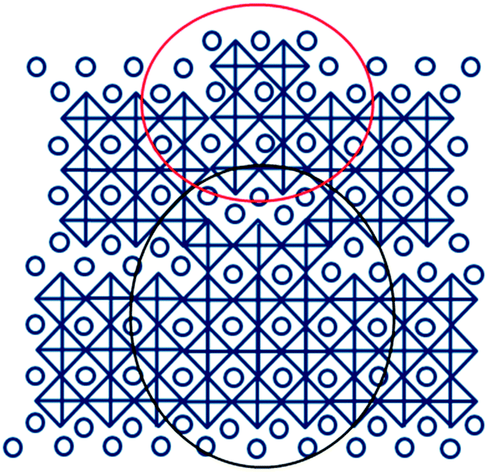 | ||
| Fig. 4 The possible structure of Bi4Ti3O12 (n = 3) phase near the OPB's formed at relative Ti/Fe flow rate of 3/0.30. The presence of half-unit cells of Bi5Ti3FeO15 causes a phase difference of nearly 4 Å, producing OPB's. In this figure titanium/iron (iron in case of films prepared with finite iron precursor flows) and oxygen atoms are at the center of octahedrons respectively and bismuth atomic positions are shown as circles. The large black and blue circles indicate BTO and BTFO half-unit cells respectively. | ||
An analysis of the intensity of the impurity peak from the Bi2Ti4O11 (B2T4O) phase for the films with a Fe/Ti ratio of 3/0.3 showed that the volume of BTO phase was 5.22 times more than B2T4O phase. These calculations were performed using structure factors for (−406) B2T4O and (00![[6 with combining low line]](https://www.rsc.org/images/entities/char_0036_0332.gif) ) BTO peaks, taking the Lorentz-polarization factor into account and considering that the absorption coefficient of both phases was identical. All calculations were tested by comparing the intensity of (008) and (00) BTO peaks and the relative error was below 2% between the values calculated and experimental values. The molar percentage of BTO and B2T4O phase was approximately 81% and 19% respectively as calculated from volume percentage. It may be assumed that there are 100 Ti and 10 Fe atoms forming the whole BTO (including OPB's) and B2T4O systems (as the Ti/Fe ratio was 3/0.3 and assuming that the Fe and Ti precursor efficiency is 100%).38 A simple calculation shows that approximately 81 Ti atoms will form BTO phase and 19 atoms will form B2T4O phase and for every half BTFO unit cells there will be 1.7 half BTO unit cells.
) BTO peaks, taking the Lorentz-polarization factor into account and considering that the absorption coefficient of both phases was identical. All calculations were tested by comparing the intensity of (008) and (00) BTO peaks and the relative error was below 2% between the values calculated and experimental values. The molar percentage of BTO and B2T4O phase was approximately 81% and 19% respectively as calculated from volume percentage. It may be assumed that there are 100 Ti and 10 Fe atoms forming the whole BTO (including OPB's) and B2T4O systems (as the Ti/Fe ratio was 3/0.3 and assuming that the Fe and Ti precursor efficiency is 100%).38 A simple calculation shows that approximately 81 Ti atoms will form BTO phase and 19 atoms will form B2T4O phase and for every half BTFO unit cells there will be 1.7 half BTO unit cells.
On further increasing the flow rate of iron precursor (Ti/Fe ratio 3/0.57). The split in (004) and (00) peaks of BTO structure gets larger. The B2T4O impurity phase still occurs in the films, but the position of the (−406) peak shifts to a slightly higher 2theta position from 42.84° to 43°, indicating a reduction in d-spacing by 0.35%. The shift in (−406) peak is probably due to the doping of B2T4O with iron which could lead to a lattice parameter reduction because of the ionic radius of Fe3+ (55 pm low spin state) is smaller than Ti4+ (60.5 pm).39 There can be two possible reasons for the wider peak split observed in (004) and (00) peaks: the first could be the presence of a higher OPB density, which usually gives rise to higher peak splitting.35,36 The second possibility can be the presence of a fractional n Aurivillius phase Bi9Ti6FeO2740 (n = 3.5), which could form due to the intergrowth of ‘n = 3’ BTO and ‘n = 4’ BTFO Aurivillius structures as the peak position matches to this phase.
The Ti/Fe ratio during the film growth is 5.26, which is slightly lower (more iron) than the required stoichiometric ratio of 6, for n = 3.5 Aurivillius phase growth. Cross-sectional HRTEM was performed on samples with a Ti/Fe ratio of 3/0.57 in order to deduce the reason of wider peak splitting. Fig. 5 shows the local crystalline structure of this film. In Fig. 5, white lines are drawn to represent bismuth oxide layers and number 3, 4 represents half unit-cells of BTO and BTFO respectively. As can be observed that in this image, the n = 3 and 4 layers have random stacking, instead of alternate stacking as in the case of Bi9Ti6FeO27 phase.40 We can still observe a few OPB's (shown by red color), but the density of OPB's is much lower when compared with the films prepared with Ti/Fe ratio 3/0.3. Thus the presence of extra iron in the films results in the formation of B2T4O impurity and also causes the random stacking of half-unit cells of n = 3 and 4 Aurivillius phase.
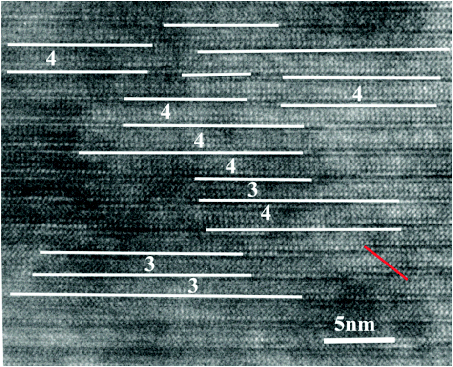 | ||
| Fig. 5 The high resolution TEM image of BTO film with Ti/Fe ratio 3/0.57. | ||
As the Ti/Fe ratio reaches 3/0.80 on further increasing the iron flow rate, there is a nucleation of the n = 4 BTFO phase. Fig. 2 shows the presence of B2T4O impurity phase, with (−406) peak further shifting to higher 2theta value (43.08), indicating the further reduction of the d-spacing of B2T4O phase by 0.53% (from B2T4O phase formed at Ti/Fe ratio 3/0.3). The pure BTFO phase forms when the Ti/Fe ratio becomes 3/1 or more, without formation of any impurity phase. Fig. 6 shows the cross-sectional high resolution TEM image for the four layered BTFO thin films.
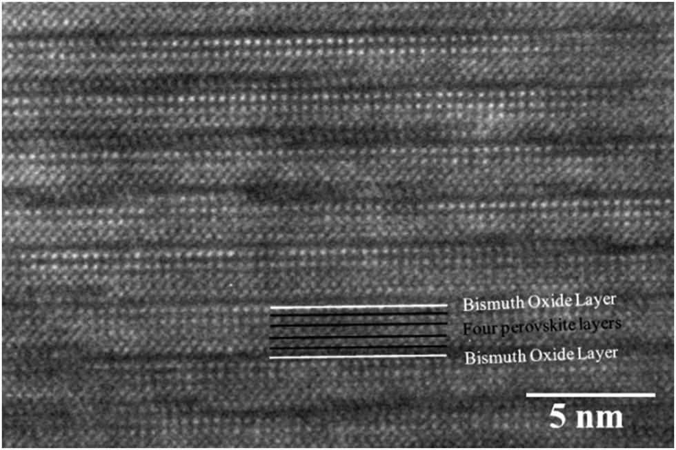 | ||
| Fig. 6 The four layered Bi5Ti3FeO15 structure shown in high resolution TEM image with four perovskite layers sandwiched between two bismuth oxide layers. | ||
The c-axis lattice parameters were calculated from XRD peaks (008), (009), and (00![[0 with combining low line]](https://www.rsc.org/images/entities/char_0030_0332.gif) ) for BTO, Bi9Ti6FeO27, and BTFO thin films respectively. All peak positions were calibrated with the substrate peaks. The change in c-axis lattice parameters for various compounds formed at from BTO to BTFO is shown in Table 1.
) for BTO, Bi9Ti6FeO27, and BTFO thin films respectively. All peak positions were calibrated with the substrate peaks. The change in c-axis lattice parameters for various compounds formed at from BTO to BTFO is shown in Table 1.
| Compound | Lattice parameter c (Å) |
|---|---|
| Bi4Ti3O12 | 32.274 |
| Bi9Ti6FeO27 | 36.454 |
| Bi5Ti3FeO15 | 40.727 |
The surface morphology of the films also changes appreciably with varying iron content. Fig. 7 shows the AFM images of the surface of the film at various Ti/Fe ratios. The RMS roughness values are also plotted against Ti/Fe ratios and are shown in Fig. 7f. The roughness of films first increases from 1.2 nm for pure BTO phase (no iron) to 1.715 nm for BTFO (Ti/Fe ratio 3/0.80). The roughness decreases drastically for pure BTFO films. The increase in RMS roughness can be attributed to the presence of impurity phase and increase in grain size.
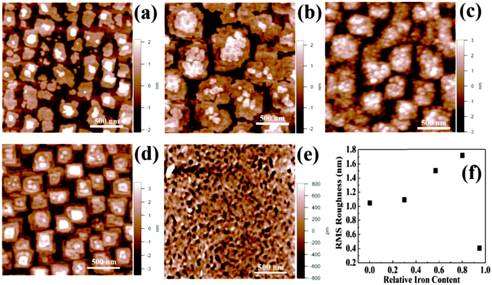 | ||
| Fig. 7 The change in surface morphology of thin films at Ti/Fe ratios (a) 3/0.0, (b) 3/0.3, (c) 3/0.57, (d) 3/0.80, and (e) Ti/Fe 3/0.95. (f) A plot showing RMS roughness values at various Ti/Fe ratios. | ||
BTFO and BTO thin films grow epitaxially with epitaxial relation (001) [001] BTO, BTFO∥(001) [001] STO and (100) [010] BTO, BTFO∥[110] STO. The BTO41 structure has smaller a–b lattice parameters (5.450 Å and 5.4059 Å) as compared with the BTFO42 structure (5.4698 Å and 5.4389 Å). Pure BTO thin film grows on STO in Stranski–Krastanov growth mode.43 This 3-D island formation on the surface of substrate occurs due to a larger lattice-mismatch of 1.7% (average) between film and STO substrate along a–b direction. The average lattice mismatch decreases to 1.2% between BTFO and STO. The BTFO films grow in layer-by-layer growth mode due to smaller lattice mismatch. In short, STO substrate provides a better epitaxial relation for BTFO films and hence results in RMS values less than 0.5 nm. These values are lowest ever reported for any form of BTFO thin films prepared.
4. Conclusions
Phase pure BTO and BTFO thin films were successfully prepared using liquid injection CVD, or AVD, in which very precise control of precursor delivery to the substrate surface is possible. XRD analysis shows films are highly c-axis oriented. It has been found that various phases occur at different iron precursor injection volumes at constant Bi and Ti values. Starting from no iron, pure BTO phase occurs. The small introduction of Fe3+ into BTO structure causes a splitting of the (004) and (0012) peaks due to formation of OPB's, as conformed by TEM analysis. The origin of OPB's was deduced from TEM images. A random occurrence of BTFO in BTO structure causes a phase shift between two layers of BTO layers and causes OPB's to appear. The fractional n = 3.5 Aurivillius phase compound Bi9Ti6FeO27, which form due to the intergrowth of BTO and BTFO, was observed to be present when growth was performed at Ti/Fe ratios of 6. A precise control over structural disorder was shown in these strategically important Aurivillius phase materials. A plausible mechanism for the transformation of n = 3 (BTO) to n = 4 (BTFO) structure is proposed. AFM analysis shows that the surface RMS roughness decreases from BTO to BTFO films due to a decrease in lattice mismatch between films and substrates. The lowest value of RMS roughness of BTFO thin films is reported as compared to other reported values in literature. This method can open up a way to fabricate and test the solubility of various ions in more complex and higher ‘n’ Aurivillius structures for next generation electronic devices.Acknowledgements
The authors acknowledge ICGEE (International Centre for Graduate Education in Micro & Nano Engineering) for funding Nitin Deepak's PhD. The support of Science Foundation Ireland (SFI) under the FORME Strategic Research Cluster Award number 07/SRC/I1172 is greatly acknowledged. In addition this work is also supported by Science foundation Ireland Principal Investigator Grant Number 11/PI/1117 (Martyn Pemble). This research was also enabled by the Higher Education Authority Program for Research in Third Level Institutions (2007–2011) via the INSPIRE program.Notes and references
- J. F. Scott, Nat. Mater., 2007, 6, 256–257 CrossRef CAS PubMed.
- E. Y. Tsymbal, A. Gruverman, V. Garcia, M. Bibes and A. Barthélémy, MRS Bull., 2012, 37, 138–143 CrossRef CAS.
- H. Masanobu, A. Takahiro, H. Kenji, L. Gyu Chang, P. Young Chul, O. Teiko and F. Yasubumi, Smart Mater. Struct., 2006, 15, N124 CrossRef.
- Y. Chen, S. M. Gillette, T. Fitchorov, L. Jiang, H. Hao, J. Li, X. Gao, A. Geiler, C. Vittoria and V. G. Harris, Appl. Phys. Lett., 2011, 99, 042505 CrossRef.
- T. Reji, J. F. Scott, N. B. Dwarka and S. K. Ram, J. Phys.: Condens. Matter, 2010, 22, 423201 CrossRef PubMed.
- E. Ascher, H. Rieder, H. Schmid and H. Stössel, J. Appl. Phys., 1966, 37, 1404–1405 CrossRef CAS.
- G. A. Smolensky, A. I. Agranovskaya and V. A. Isupov, Sov. Phys. Solid State, 1959, 1, 149 Search PubMed.
- N. A. Hill, J. Phys. Chem. B, 2000, 104, 6694–6709 CrossRef CAS.
- F. Manfred, J. Phys. D: Appl. Phys., 2005, 38, R123 CrossRef.
- J. Wang, J. B. Neaton, H. Zheng, V. Nagarajan, S. B. Ogale, B. Liu, D. Viehland, V. Vaithyanathan, D. G. Schlom, U. V. Waghmare, N. A. Spaldin, K. M. Rabe, M. Wuttig and R. Ramesh, Science, 2003, 299, 1719–1722 CrossRef CAS PubMed.
- G. Srinivasan, E. T. Rasmussen, B. J. Levin and R. Hayes, Phys. Rev. B: Condens. Matter Mater. Phys., 2002, 65, 134402 CrossRef.
- J. Zhai, Z. Xing, S. Dong, J. Li and D. Viehland, Appl. Phys. Lett., 2006, 88, 062510 CrossRef.
- J. Ryu, A. V. Carazo, K. Uchino and H. E. Kim, Jpn. J. Appl. Phys., Part 1, 2001, 40, 4948–4951 CrossRef CAS.
- S. Dong, J. Cheng, J. F. Li and D. Viehland, Appl. Phys. Lett., 2003, 83, 4812–4814 CrossRef CAS.
- P. Record, C. Popov, J. Fletcher, E. Abraham, Z. Huang, H. Chang and R. W. Whatmore, Sens. Actuators, B, 2007, 126, 344–349 CrossRef CAS.
- S. Dong, J.-F. Li and D. Viehland, Appl. Phys. Lett., 2003, 83, 2265–2267 CrossRef CAS.
- H. Zheng, J. Wang, S. E. Lofland, Z. Ma, L. Mohaddes-Ardabili, T. Zhao, L. Salamanca-Riba, S. R. Shinde, S. B. Ogale, F. Bai, D. Viehland, Y. Jia, D. G. Schlom, M. Wuttig, A. Roytburd and R. Ramesh, Science, 2004, 303, 661–663 CrossRef CAS PubMed.
- S. Valencia, A. Crassous, L. Bocher, V. Garcia, X. Moya, R. O. Cherifi, C. Deranlot, K. Bouzehouane, S. Fusil, A. Zobelli, A. Gloter, N. D. Mathur, A. Gaupp, R. Abrudan, F. Radu, A. Barthélémy and M. Bibes, Nat. Mater., 2011, 10, 753–758 CrossRef CAS PubMed.
- W. Eerenstein, M. Wiora, J. L. Prieto, J. F. Scott and N. D. Mathur, Nat. Mater., 2007, 6, 348–351 CrossRef CAS PubMed.
- L. Keeney, T. Maity, M. Schmidt, A. Amann, N. Deepak, N. Petkov, S. Roy, M. E. Pemble and R. W. Whatmore, J. Am. Ceram. Soc., 2013, 96, 2339–2357 CrossRef CAS.
- B. Aurivillius, Ark. Kemi, 1949, 1, 463 CAS.
- B. Aurivillius, Ark. Kemi, 1950, 2, 519 CAS.
- M. Krzhizhanovskaya, S. Filatov, V. Gusarov, P. Paufler, R. Bubnova, M. Morozov and D. C. Meyer, Z. Anorg. Allg. Chem., 2005, 631, 1603–1608 CrossRef CAS.
- A. Srinivas, D.-W. Kim, K. S. Hong and S. V. Suryanarayana, Appl. Phys. Lett., 2003, 83, 2217–2219 CrossRef CAS.
- F. Huang, X. Lu, T. Xu, Y. Liu, W. Su, Y. Jin, Y. Kan and J. Zhu, Thin Solid Films, 2012, 520, 6489–6492 CrossRef CAS.
- X. Mao, W. Wang, X. Chen and Y. Lu, Appl. Phys. Lett., 2009, 95, 082901 CrossRef.
- W. Bai, W. F. Xu, J. Wu, J. Y. Zhu, G. Chen, J. Yang, T. Lin, X. J. Meng, X. D. Tang and J. H. Chu, Thin Solid Films, 2012, 525, 195–199 CrossRef CAS.
- W. Bai, J. Y. Zhu, J. L. Wang, T. Lin, J. Yang, X. J. Meng, X. D. Tang, Z. Q. Zhu and J. H. Chu, J. Magn. Magn. Mater., 2012, 324, 2265–2270 CrossRef CAS.
- L. Keeney, S. Kulkarni, N. Deepak, M. Schmidt, N. Petkov, P. F. Zhang, S. Cavill, S. Roy, M. E. Pemble and R. W. Whatmore, J. Appl. Phys., 2012, 112, 052010 CrossRef.
- M. Schmidt, A. Amann, L. Keeney, M. E. Pemble, J. D. Holmes, N. Petkov and R. W. Whatmore, Sci. Rep., 2014, 4, 5712 CAS.
- H. M. Christen and G. Eres, J. Phys.: Condens. Matter, 2008, 20, 1–16 CrossRef PubMed.
- B. A. Joyce, Rep. Prog. Phys., 1985, 48, 1637–1697 CrossRef CAS.
- M. Leskela and M. Ritala, Thin Solid Films, 2002, 409, 138–146 CrossRef CAS.
- K. L. Choy, Prog. Mater. Sci., 2003, 48, 57–170 CrossRef CAS.
- N. Deepak, P. F. Zhang, L. Keeney, M. E. Pemble and R. W. Whatmore, J. Appl. Phys., 2013, 113, 187207 CrossRef.
- M. A. Zurbuchen, W. Tian, X. Q. Pan, D. Fong, S. K. Streiffer, M. E. Hawley, J. Lettieri, Y. Jia, G. Asayama, S. J. Fulk, D. J. Comstock, S. Knapp, A. H. Carim and D. G. Schlom, J. Mater. Res., 2007, 22, 1439–1471 CrossRef CAS.
- S. Y. Yang, F. Zavaliche, L. Mohaddes-Ardabili, V. Vaithyanathan, D. G. Schlom, Y. J. Lee, Y. H. Chu, M. P. Cruz, Q. Zhan, T. Zhao and R. Ramesh, Appl. Phys. Lett., 2005, 87, 102903 CrossRef.
- P. F. Zhang, N. Deepak, L. Keeney, M. E. Pemble and R. W. Whatmore, Appl. Phys. Lett., 2012, 101, 112903 CrossRef.
- R. Shannon, Acta Crystallogr., Sect. A: Cryst. Phys., Diffr., Theor. Gen. Crystallogr., 1976, 32, 751–767 CrossRef.
- G. N. Subbanna, T. N. G. Row and C. N. R. Rao, J. Solid State Chem., 1990, 86, 206–211 CrossRef CAS.
- A. D. Rae, J. G. Thompson, R. L. Withers and A. C. Willis, Acta Crystallogr., Sect. B: Struct. Crystallogr. Cryst. Chem., 1990, 46, 474–487 CrossRef.
- C. H. Hervoches, A. Snedden, R. Riggs, S. H. Kilcoyne, P. Manuel and P. Lightfoot, J. Solid State Chem., 2002, 164, 280–291 CrossRef CAS.
- G. W. Brown, M. E. Hawley, C. D. Theis, J. Yeh and D. G. Schlom, Thin Solid Films, 1999, 357, 13–17 CrossRef CAS.
| This journal is © The Royal Society of Chemistry 2015 |