
 Open Access Article
 This Open Access Article is licensed under a
 Creative Commons Attribution 3.0 Unported Licence
The controlled deposition of Cu2(ZnyFe1−y)SnS4, Cu2(ZnyFe1−y)SnSe4 and Cu2(ZnyFe1−y)Sn(SxSe1−x)4 thin films by AACVD: potential solar cell materials based on earth abundant elements†
Punarja
Kevin
a,
Mohammad Azad
Malik
*b and
Paul
O'Brien
*ab
aSchool of Chemistry, The University of Manchester, Oxford Road, M13 9PL, UK
bSchool of Materials, The University of Manchester, Oxford Road, M13 9PL, UK. E-mail: azad.malik@manchester.ac.uk
First published on 5th May 2015
Abstract
Highly crystalline thin films of Cu2(ZnyFe1−y)SnS4 (CZFTS), Cu2(ZnyFe1−y)SnSe4 (CZFTSe) and Cu2(ZnyFe1−y)Sn(SxSe1−x)4 (CZFTSSe) have been deposited by aerosol assisted chemical vapour deposition (AACVD) from mixtures of dithio- or diseleno-carbamato, diselenophosphinato and acetylacetenato complexes. The structure, morphology, composition, optical and electrical properties of the deposited materials were investigated. The [Zn]![[thin space (1/6-em)]](https://www.rsc.org/images/entities/char_2009.gif) :[Fe] and [S]:[Se] ratios are the important factors affecting the overall properties of these materials and can be controlled.
:[Fe] and [S]:[Se] ratios are the important factors affecting the overall properties of these materials and can be controlled.
Introduction
Kesteric materials are considered to be amongst the better of the new absorbers for polycrystalline PV-solar cells.1 The parent family encompasses Cu2ZnSnS4 (CZTS Kesterite), Cu2ZnSn(SxSe1−x)4, (CZTSSe) and Cu2ZnSnSe4 (CZTSe).1 The related iron containing phases Cu2(ZnyFe1−y)SnS4 (CZFTS), Cu2(ZnyFe1−y)SnSe4 (CZFTSe) and (CZFTSSe) have optical band gaps, large absorption coefficient and transport properties similar to those of CZTS.2–4 There are few studies reported for materials that can form in both the kesteritic (space group I![[4 with combining macron]](https://www.rsc.org/images/entities/char_0034_0304.gif) 8m) and the stannitic (space group I2m) type dependent upon the [Zn]:[Fe] ratio.4 The polymorphs have very small difference in thermodynamic stability. The addition of iron into CZTS thin films decreases the optical band gap which can improve the power conversion efficiency (PCE) of thin film solar cells (TFSCs). The solubility of iron in the CZTS derivatives plays a key role in controlling many parameters.5
8m) and the stannitic (space group I2m) type dependent upon the [Zn]:[Fe] ratio.4 The polymorphs have very small difference in thermodynamic stability. The addition of iron into CZTS thin films decreases the optical band gap which can improve the power conversion efficiency (PCE) of thin film solar cells (TFSCs). The solubility of iron in the CZTS derivatives plays a key role in controlling many parameters.5
The iron containing analogues are of particular interest for Si-based tandem solar cells as the lattice constant of Si (5.4311 Å) lies between two end members in the Cu2(ZnyFe1−y)Sn(SxSe1−x)4 series CFTS (5.414 Å) to CZTSe (5.435 Å). Variations in [Zn]:[Fe], or [S]:[Se] composition affect both the lattice spacing's and band gap.2–6 The magnetic5 and vibrational7 properties of CZFTS alloys have also been investigated. Addition of Fe in CZTS thin films decreases the optical band gap energy which can improve the PCE of TFSCs.2 Nanocrystals of the related CuInxGa1−x(SySe1−y)2 (CIGSSe) synthesized by colloidal methods, have band gaps tunable from 0.98–2.40 with changes in x and y from 0 to 1.8
AACVD is a simple technique which can operate at an ambient-pressure using the nebulization of the precursor molecules, followed by transport of the aerosol by an inert carrier gas such as argon or nitrogen to a substrate surface heated in a furnace where thermal decomposition of the precursor occurs.
AACVD has been widely applied in the deposition of complex systems and has enabled the used of less volatile precursors than more conventional CVD methods. These have included high temperature superconductors9 and other oxides.9 Stoichiometry controlled thin films of CdS, ZnS, and Cd1−xZnxS were deposited from Cd(SOCCH3)2–TMEDA and Zn(SOCCH)2–TMEDA (TMEDA = N,N,N,N-tetramethylethylenediamine).9 Marks et al. reported the deposition of metallic silver thin films using tris(phosphino)boratosilver(I) complexes10 and Parkin et al. reported a single step route to the deposition of super hydrophobic surfaces through AACVD and deposition of ZnO thin films by AACVD.11 Wijayantha et al. reported the polycrystalline a-Fe2O3 electrodes by aerosol-assisted chemical vapour deposition from a ferrocene precursor.12 Mazhar et al. reported the deposition of high quality NiTiO3 thin films from a single-source heterobimetallic complex [Ni2Ti2(OEt)2(m-OEt)6(acac)4] precursor.13 The method has also been successfully applied for α-Fe2O3 using [Fe6(PhCOO)10(acac)2(O)2(OH)2]33C7H8.14 AACVD has recently been used for the deposition of various semiconductor materials including SnS,15 CZTS,16 CuInSe2,17 CuGaSe2,17 CuIn0.7Ga0.3Se,17 MoS2,18 inorganic–organic perovskite (CH3NH3)PbBr3,19 SnSe and Cu2SnSe3.19 Hussain et al. reported different morphologies of hexagonal FeSe from 1-benzoyl-3-(4-ferrocenylphenyl)selenourea under the influence of surfactants (span and triton) and temperature.20 Very recently bismuth vanadate (BiVO4) thin film photoelectrodes prepared by AACVD on fluorine doped tin oxide (FTO) glass substrates were produced, BiVO4 photoelectrodes is promising for use in PEC water-splitting cells.21 Recently the application of AACVD has been reviewed by Marchand et al.9 β-In2S3 thin films deposited by AACVD, irrespective of different metal ligand design, generate comparable morphologies of thin films at different temperatures, the measured photoelectrochemical performance of these films were highly useful in fabricating electrodes for solar energy harvesting and optoelectronic application.22
Dhurba and reported the deposition of CZFTS thin films, by spray pyrolysis followed by sulfurization at ∼500 °C.7 Agawane et al. reported the effect of [Zn]:[Fe] ratio on the properties of CZFTS thin films deposited by a pulsed laser deposition technique but the formation of Cu-rich and Zn-poor large grains was found to affect these parameters.2 We have used a series of molecular precursors for the deposition of binary and ternary materials.22 Herein, we report the AACVD of CZFTS, CZFTSe and CZFTSSe thin films and detailed investigation on the effect of [Zn]:[Fe] and [S]:[Se] ratios on the structure, morphology, optical band gap and electrical resistance of these materials.
Experimental section
Preparations were performed under an inert atmosphere of dry nitrogen using standard Schlenk techniques. All reagents were purchased from Sigma-Aldrich chemical company and used as received. Solvents were distilled prior to use. Elemental analysis was performed by the University of Manchester micro-analytical laboratory. TGA measurements were carried out by a Seiko SSC/S200 model from 10 to 600 °C with a heating rate of 10 °C min−1 under nitrogen. Melting point was recorded on a Stuart melting point apparatus and uncorrected.Synthesis of metal–organic complexes
The compounds [Cu(S2CNEt2)2], [Fe(S2CNEt2)3], [nBu2Sn(S2CNEt2)2], [Zn(S2CNEt2)2], [Zn(Se2CNEt2)2] and [Cu(PPh3)(Ph2P(Se)NP(Se)Ph2)] were synthesised and recrystallized as reported in literature, brief details follow.14,23–25Deposition of thin films
The thin films were deposited using AACVD. Glass slides (1 × 2 cm) were used as substrates for the deposition of thin films. Substrates were thoroughly cleaned and sonicated in acetone for 30 minutes to remove any possible contamination. In a typical deposition experiment, precursor complex (or a suitable combination of precursors) was dissolved in 20 mL THF taken in a two-necked 100 mL round-bottom flask. The round-bottom flask was kept in a water bath above the piezoelectric modulator of a PIFCO ultrasonic humidifier (model 1077). The aerosol droplets of the precursor thus generated were transferred into the hot wall zone of the reactor by a carrier gas (Argon). The Argon flow rate was controlled at 180 sccm by a Platon flow gauge. Both the solvent and precursor were evaporated, and the precursor vapor reached the heated substrate surface where thin film was deposited at 300–400 °C.Deposition of CZFTS thin films
Thin films of Cu2(ZnyFe1−y)SnS4 (CZFTS) were deposited using a mixture of [Cu(S2CNEt2)2] (2.78 mmol), [Fe(S2CNEt2)3] (0.7 mmol), [Zn(S2CNEt2)2] (0.7 mmol) and [nBu2Sn(S2CNEt2)2] (1.40 mmol) in the molar ratio 2:1:0.5:0.5:1 in 20 ml THF. The AACVD experiments were carried out as described above at 300 and 350 °C. The Fe-rich compositions of this material were deposited by increasing the ratio of the iron precursor as compared to that of zinc precursor. A mixture of [Cu (S2CNEt2)2] (2.78 mmol), [Fe(S2CNEt2)3] (1.0 mmol), [Zn(S2CNEt2)2] (0.4 mmol) and [nBu2Sn(S2CNEt2)2] (1.40 mmol) in 2:1:0.7:0.3:1 molar ratio in 20 ml THF was used to deposit films at 350 °C.
Deposition of CZFTSe thin films
The deposition of Cu(ZnFe)SnSe4 was carried out by using a mixture of [Cu(PPh3)(Ph2P(Se)NP(Se)Ph2)], (2.78 mmol), [Sn(CH3CO2)4] (1.40 mmol) [Zn(Se2CNEt2)2] (0.7 mmol) and [Fe(acac)3] (0.7 mmol) in the molar ratio 2:1:0.5:0.5:1 in 20 mL of THF at 300 °C and 350 °C for 55 minutes. For the deposition of Fe-rich films a similar deposition was carried out at 350 °C with different ratio of [Zn(S2CNEt2)2] (0.4 mmol) (2.8 mmol) and [Fe(acac)3] (1.0 mmol) in 2:1:0.7:0.3:1 molar ratio in 20 mL THF and keeping other precursor concentrations same as in the previous experiment.
Deposition of CZFTSSe thin films
The Cu2(ZnyFe1−y)Sn(SxSe1−x)4 thin films were deposited by using [Zn(Se2CNEt2)2] (0.7 mmol) whilst keeping all the other precursors same as for Zn-rich CZFTS (1:0.5:0.5:1 in 20 mL of THF). The depositions were carried out at 300 °C and 350 °C. For the deposition of Fe-rich composition on the films, another deposition was carried out at 350 °C using [Zn(Se2CNEt2)2] (0.4 mmol) and [Fe(S2CNEt2)3] (1.0 mmol) in 2:1:0.7:0.3:1 molar ratio in 20 mL THF whilst keeping all the other concentrations same.
Characterisation of thin films
The p-XRD patterns were recorded on a Bruker D8 AXE diffractometer using Cu-Kα radiations. The samples were mounted flat and scanned between 10 and 120° in a step size of 0.05 with a varying count rate depending upon the sample. The morphology and microstructure of thin films were investigated by using a Philips XL 30 FEGSEM and film composition was studied by EDX analysis using a DX4 instrument at 20 kV with WD 10 mm. Raman spectra measurements taken in Renishaw 1000 Micro Raman system with an excitation wavelength of 520 nm, measurement range set from 100 to 700 cm−1. UV-VIS measurement carried out in Perkin Elmer Lambda 1050 spectrophotometer (PSI), scanned across the range from 250–1000 nm. Electrical resistance measured using Jandel four probe conductivity meter under room temperature using 1 μA current. TEM samples were prepared by evaporating a drop of a dilute suspension of the sample in toluene or hexane on carbon coated copper grid. The excess solvent was allowed to dry completely at room temperature. TEM images and elemental maps were collected on Technai T20 microscope using accelerating voltage of 300 kV. TEM (nanoscale) elemental maps were measured using Aztec software.Results and discussion
Thermal decomposition studies
Thermal decomposition studies were carried at 10–600 °C; heating rate 10 °C min−1 under nitrogen. All compounds show rapid single step decomposition between 250–350 °C (Fig. 1). The residual mass of [Fe(S2CNEt2)3] complex found to be about 18% which close to the calculated percentage of FeS (17.5%). The [Bu2Sn(S2CNEt2)2] complex decomposed slightly faster than the other complexes and the residual mass found to be ∼34% which agrees with the calculated residual mass of SnS2. [Zn(S2CNEt2)2] and [Zn(Se2CNEt2)2] resulted with ∼9–10% residue which found to be half or less than half of the mass of the expected metal chalcogenides; ZnS (27%) and ZnSe (20%). TGA of [Cu(PPh3)(Ph2P(Se)NP(Se)Ph2)] showed single step decomposition between 250 to 320 °C with residue ∼10% which was lesser than the expected residual mass of CuSe (16%).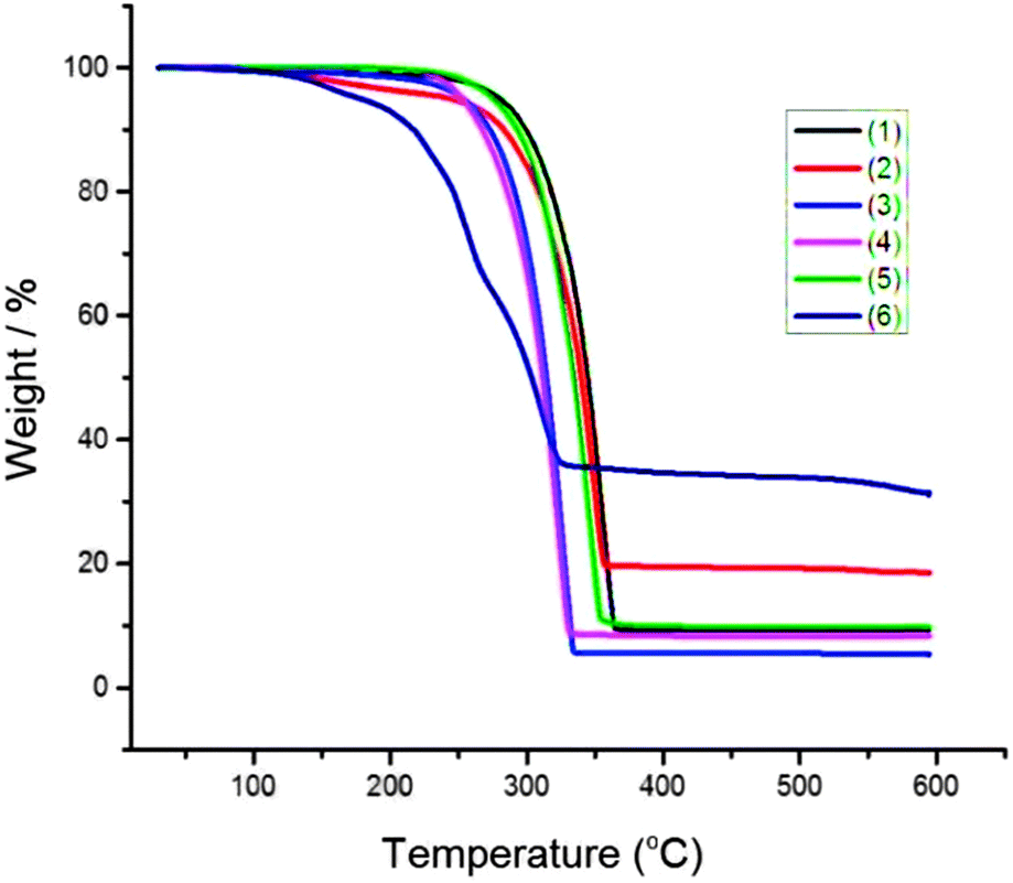 | ||
| Fig. 1 TGA of [Cu(S2CNEt2)2] (1), [Fe(S2CNEt2)3] (2), [Zn(S2CNEt2)2] (3), [nBu2Sn(S2CNEt2)2] (4), [Zn(Se2CNEt2)2] (5) and [Cu(PPh3)(Ph2P(Se)NP(Se)Ph2)] (6) complexes. | ||
X-ray diffraction studies
The deposition of CZFTS materials at 300 °C gave very thin dark green films which did not diffract whereas black adherent films were deposited at 350 °C. The p-XRD pattern (Fig. 2) of these films was corresponding to the Zn-rich phase of Cu2Fe0.3Zn0.7Sn1S4 (ICDD 04-015-0225) with the tetragonal space group I2m with lattice parameters a = 5.42(2) Å and c = 10.86(4) Å. Rietveld refinement carried out on the p-XRD patterns of the deposited material using this Zn-rich standard space group showed very good fit with a Rietveld parameter Rwp = 2.85, space group I2m with lattice parameters a = 5.411(4) Å and c = 10.862(3) Å (Fig. 3(a)). The main d-spacing for the planes were 3.13 Å (112), 1.91 Å (204), 1.91 Å (220), 1.63 Å (116) and 1.63 Å (312) respectively. The resultant d-spacing were well matched with the reported d-spacing for the corresponding planes at 3.13 Å (112), 1.91 Å (204), 1.91 Å (220), 1.63 Å (116) and 1.63 Å (312) respectively (ICDD: 04-015-0225) for Cu2Fe0.3Zn0.7Sn1S4. The doublet planes were not well resolved possibly due to broadening of the peaks due to the small size of the particles compared to the bulk materials, but the material is very close to cubic. The details of calculated d-spacings and 2θ values are shown in Table S1 in the ESI.† The lattice parameters also estimated calculated from the principal peaks in the p-XRD patterns to a cubic cell giving a = 5.412(8) Å in good agreement with the values obtained from the Rietveld refinement (Table 1). This approach was also used for all films some of which did not give good fits in the Rietveld analysis.
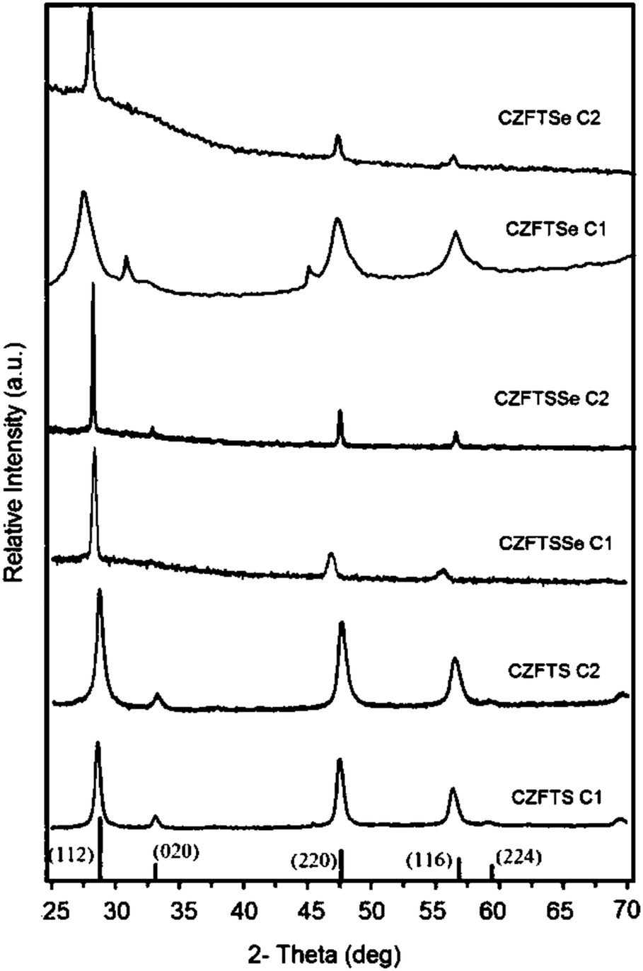 | ||
| Fig. 2 p-XRD patterns of Zn-rich (C1) and Fe-rich (C2) phases of CZFTS, CZFTSe, CZFTSSe thin films deposited with different [Zn] at 350 °C. | ||
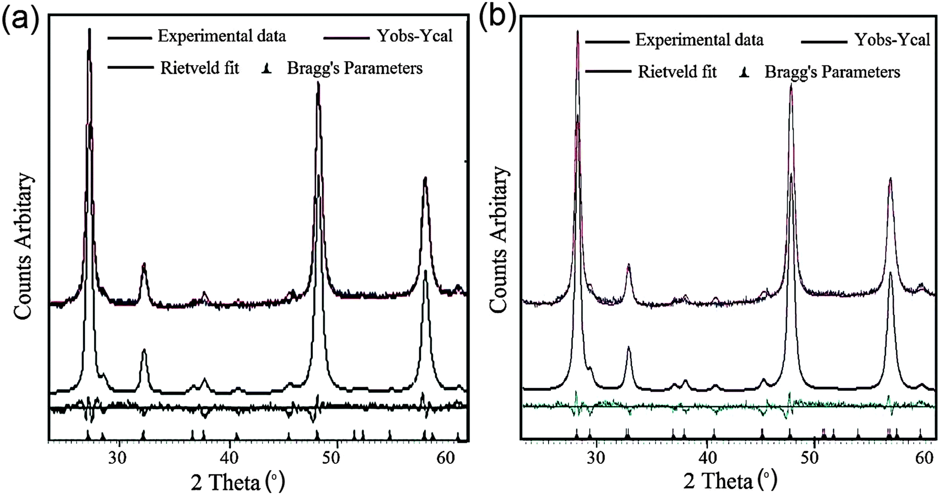 | ||
| Fig. 3 (a) Rietveld analysis p-XRD patterns of CZFTS thin films deposited at 350 °C using 2:1:0.5:0.5:1 of [Cu(S2CNEt2)2]:[Fe(S2CNEt2)3]:[Zn(S2CNEt2)2]:[nBu2Sn(S2CNEt2)2] precursors. The peaks fitted using Cu2Fe0.3Zn0.7Sn1S4 (ICDD 04-015-0225) phase. (b) Rietveld analysis of p-XRD patterns of CZFTS thin films deposited at 350 °C using 2:1:0.7:0.3:1 of [Cu(S2CNEt2)2]:[Fe(S2CNEt2)3]:[Zn(S2CNEt2)2]:[nBu2Sn(S2CNEt2)2] precursors. The peaks fitted using Fe-rich Cu2Fe0.7Zn0.3Sn1S4 (ICDD: 01-015-0228) phase. | ||
| Sample | T (°C) | [Cu] AACVD | [Cu] EDX | [Zn] AACVD | [Zn] EDX | [Sn] AACVD | [Sn] EDX | [Fe] AACVD | S EDX | Se EDX | a (Å) Riet | c (Å) Riet | a (Å) hkl | BG/eV | R/Ω |
|---|---|---|---|---|---|---|---|---|---|---|---|---|---|---|---|
| CZFTS (C1) | 350 | 2.78 | 2.2 | 0.7 | 0.7 | 1.4 | 1.3 | 0.7 | 3.4 | 0 | 5.411(4) | 10.862(3) | 5.412(8) | 1.72 | 2.48 |
| CZFTS (C2) | 350 | 2.78 | 1.9 | 0.4 | 0.3 | 1.4 | 1.3 | 1 | 3.2 | 0 | 5.418(7) | 10.829(1) | 5.415(2) | 1.67 | 2.42 |
| CZFTSSe (C1) | 350 | 2.78 | 1.7 | 0.7 | 0.6 | 1.4 | 0.8 | 0.7 | 1.9 | 1.2 | x | x | 5.477(5) | 1.64 | 2.31 |
| CZFTSSe (C2) | 350 | 2.78 | 2 | 0.7 | 0.4 | 1.4 | 0.8 | 1 | 2.1 | 1.7 | x | x | 5.429(8) | 1.61 | 2.29 |
| CZFTSe (C1) | 350 | 2.78 | 2 | 0.7 | 0.7 | 1.4 | 1 | 0.7 | 0 | 3.1 | x | x | 5.429(7) | 1.47 | 2.21 |
| CZFTSe (C2) | 350 | 2.78 | 1.8 | 0.4 | 0.3 | 1.4 | 0.9 | 1 | 0 | 3 | x | x | 5.492(7) | 1.48 | 2.16 |
CZFTS films deposited at 350 °C using a higher ratio of the Fe precursor (CZFTS C2 in Table 1) were very dark and uniform. The p-XRD pattern of as deposited films (Fig. 3(b)) corresponds to the Fe-rich phase of Cu2Fe0.7Zn0.3Sn1S4 (ICDD: 01-015-0228). No additional phase or impurities were found in the p-XRD and showed good match to the stick patterns can be seen in Fig. 2. Rietveld refinement of the resultant p-XRD patterns analysed with the observed Fe-rich phase showed very good match with Rwp = 2.43 as shown in Fig. 3(b). The standard material possesses an I2m space group with space group number 12 and a = 5.43(2) Å and c = 10.79(4) Å and the refined space group was found to be I2m with lattice parameters a = 5.42 Å and c = 10.83 Å. The resultant d-spacing for the planes and planes were 3.13 Å (112), 1.91 Å (220) and 1.63 Å (312) which found to be the same as the standard d-spacing for the planes i.e. 3.13 Å (112), 1.91 Å (220) and 1.63 Å (312) respectively (ICDD: 01-015-0228). The details of calculated d-spacing's and 2θ positions are given in Table S2 in the ESI.† The lattice parameters a calculated from the principal peaks in p-XRD patterns were 5.415 (2) (see Table S1, ESI†).
The deposition of Cu(ZnFe)SnSe4 at 300 °C gave only amorphous material which did not show any diffraction by p-XRD whereas uniform dark brownish films were obtained at 350 °C. The p-XRD pattern of the thin films deposited at 350 °C are shown in Fig. 2, peaks show clear shifts from Zn-rich Cu2ZnFeSnS4 (ICDD: 00-83-0225) and Fe-rich Cu2ZnFeSnS4 (ICDD: 01-015-0228) phase as expected. The p-XRD pattern found to be broader because of the small particle size of individual crystallites and overlapping of peaks especially about 2θ:47 to 48° and around 2θ:55–56. The calculated lattice parameters from the p-XRD patterns was a = 5.429(7) Å (Table 1).
A similar deposition with more Fe precursor concentration at 350 °C gave thin brown films. The p-XRD patterns were analysed by comparing with the Zn-rich Cu2ZnFeSnS4 (ICDD: 00-83-0225) an Fe-rich Cu2ZnFeSnS4 (ICDD: 01-015-0228) phases (Fig. 2), it had been observed that the p-XRD patterns were shifted significantly from the reference patterns. The p-XRD patterns were further analysed using Cu2FeSnSe4 patterns (JCPDS: 00-027-0167) but none of the peaks no matching peaks were seen. The calculated lattice parameters from the p-XRD patterns was a = 5.492(7) Å (Table 1).
The deposition of Cu2(ZnFe)Sn(SxSe1−x)4 using a mixture of precursors as described in the experimental part gave only a negligible amount of deposits at 300 °C whereas good quality black specular films were deposited at 350 °C. The p-XRD pattern of these films showed a clear shifts from those of the Fe-rich and Zn-rich phases of CZFTS indicating the formation of Cu2(ZnyFe1−y)Sn(SxSe1−x)4 as shown in Fig. 2. The calculated lattice parameter a = 5.477(5) Å (Table 1). Another deposition with more Fe precursors at 350 °C produced thin black films. The p-XRD pattern was compared with Fe-rich (ICDD: 01-015-0228) and Zn-rich (ICDD 04-015-0225) CZFTS patterns. The peaks showed larger shift from both reference patterns (Fig. 2). The lattice parameter a calculated from the p-XRD patterns was 5.429(8) Å (see Table 1).
SEM, EDX and TEM studies
Elemental analysis of the films confirmed that the metal content of all films correlated well with mole fraction of metal in the feed shown in Fig. 4. It is clear from the figure shows that a correlation between the mole fraction of Se in the precursor mixture and mole fraction of Se in the deposited thin films. From the graph it shows a linear correlation between the mole fraction of Se in the precursor and in the deposited thin films.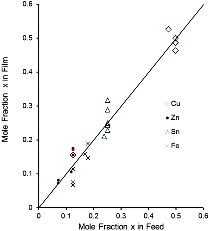 | ||
| Fig. 4 Correlation between mole fraction of each metal (x) in the feed and observed amount in the film by EDX. | ||
The SEM images of all deposited films showed different morphologies with ∼1 μm thickness over the entire area of the substrate (Fig. 5). Zn-rich phase of CZFTS thin films deposited at 350 °C showed irregular flakes, less than 1 micron thickness. Elemental map confirmed of these films the uniform distribution of elements through the entire film (Fig. 6(a)). EDX confirmed the p-XRD results by showing the deposition of the Zn-rich films: Cu (28.42%), Zn (8.84%), Fe (3.97%), Sn (15.23%), S (43.54%) corresponding to Cu2.2Fe0.3Zn0.7Sn1.2S3.4. SEM images of the CZFTS thin films deposited from higher concentration of iron precursor showed uniform flakes with an even distribution (Fig. 5(b)). EDX results revealed the composition as (Cu (25.92%) Zn (4.52%) Fe (9.5%) Sn (17.52%) S (45.54%)) giving an empirical formula of Cu1.9Fe0.7Zn0.3Sn1.3S3.2 confirming the deposition of Fe-rich films. Elemental map of the films showed uniform composition of deposited material with constituent elements are shown in Fig. 6(b).
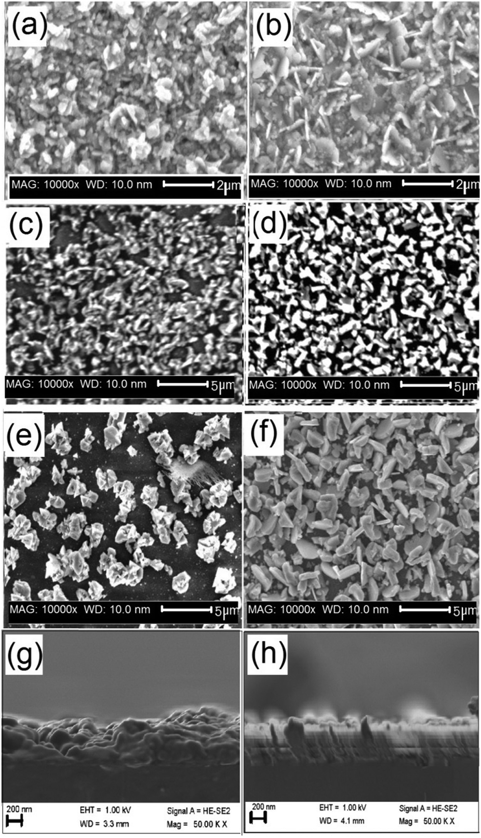 | ||
| Fig. 5 (a) and (b) are the SEM images, Zn-rich (CZFTS C1) and Fe-rich (CZFTS C2) phases of CZFTS films (c) and (d) are the SEM images, Zn-rich (CZFTSe C1) and Fe-rich (CZFTSe C2) phases of CZFTSe. (e) and (f) are the SEM images, Zn-rich (CZFTSSe C1) and Fe-rich (CSFTSSe C2) phases of CZFTSSe films deposited at 350 °C. (g) and (h) are the cross sectional images of films (a) and (b). | ||
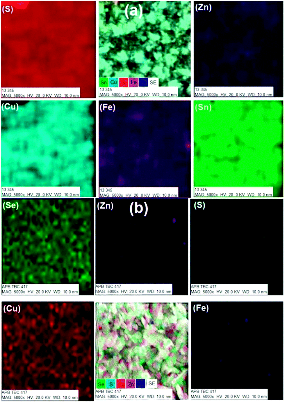 | ||
| Fig. 6 Elemental map images for (a) (CZFTS C1) and (b) Zn-rich and Fe-rich (CZFTS C2) phases of CZFTS films deposited at 350 °C. | ||
The SEM images of C(ZF)TSe thin films deposited at 350 °C showed irregular crystallites with size ca. 1 μm as shown in Fig. 5(c). EDX analysis results showed atomic percentage of Cu (28.55%), Zn (10.72%), Fe (3.55%), Sn (14.50%) and Se (42.65%) which gave a stoichiometric composition as Cu2.0Zn0.7Fe0.3Sn1.0Se3.1; a Zn-rich phase.
SEM images with Fe-rich phases of C(ZF)TSe showed irregularly shaped crystallites (Fig. 5(d)). EDX analysis showed atomic percentage of Cu (26.13%), Zn (4.10%), Fe (11.21%), Sn (13.60%) and Se (44.13%) which gives a stoichiometric composition of Cu1.8Zn0.3Fe0.7Sn0.9Se3.0 corresponding to Fe-rich phase.
The SEM images of Cu2(ZnFe)Sn(SxSe1−x)4 thin films deposited at 350 °C showed morphology based on irregular plate like crystallites as shown in Fig. 5(e). The EDX analysis showed Cu (25.63%) Zn (8.74%) Fe (6.46%) Sn (12.46%) S(28.74%) and Se (17.94%) corresponding to Cu1.7Fe0.4Zn0.6Sn0.8S1.9Se1.2, the Zn-rich and S-rich stoichiometry.
The (ZnFe)Sn(SxSe1−x)4 films deposited with higher concentration of Fe at 350 °C on EDX analysis showed Cu (26.87%) Zn (5.13%) Fe (7.92%) Sn (11.15%) S (26.24%) and Se (22.85%) corresponding to Cu2.1Fe0.6Zn0.4Sn0.8S2.1Se1.7 which showed a Fe and S-rich stoichiometry. SEM images showed irregular plate like crystallites (Fig. 5(f)). The elemental map showed uniform composition throughout the material (ESI,† Fig. S1 and S2).
The Fe-rich CZFTS thin films (CZFTS C1) and Zn-rich (CZFTS C2) phases were further studied using TEM. The films were removed by scratching and ground, and dispersed in toluene for TEM analysis. The TEM images (Fig. 7) showed flaky irregular crystallites with size ranging from 10 to 30 nm. Selected area elemental map results further revealed the Zn-rich and Fe-rich phases in the nm scale. The d-spacing obtained from lattice fringes and diffraction patterns were in good agreement with the standard patterns for the Zn-rich and Fe-rich phases.
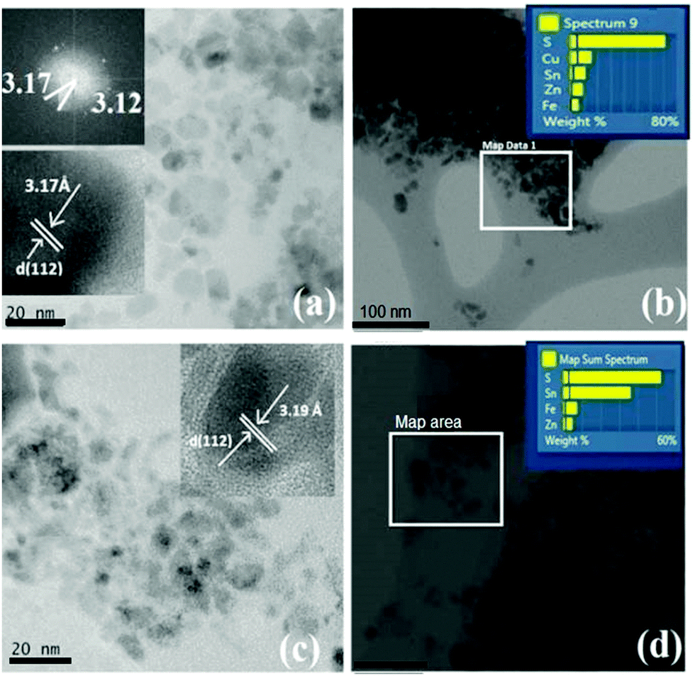 | ||
| Fig. 7 (a) and (b) shows the TEM images and elemental map of CZFTS thin films deposited using 2:0.5:0.5:1 molar ratio of Cu, Fe, Fe and Sn precursors at 350 °C (CZFTS C1). (c) and (d) shows the TEM and elemental maps of CZFTS thin films deposited with 2:0.7:0.3:1 molar ratio of Cu, Fe, Zn and Sn precursor mixture at 350 °C (CZFTS C2). Inserts images in (a) and (c) shows the d-spacing of the particles. | ||
Raman spectra and UV-visible spectra
The Raman spectra of films deposited with different [Fe]:[Zn] ratios of CZFTS, CZFTSe and CZFTSSe are shown in Fig. 8. Raman spectra showed peaks at ∼340 cm−1 and 350 cm−1 for CZFTS Fe-rich and Zn-rich phases. The Zn-rich CZFTS showed a higher Raman mode than the Fe-rich material as reported previously.2,7 Tauc plots drawn by plotting (αhν)2 against hν of films deposited with different [Fe]:[Zn] ratios of CZFTS, CZFTSe and CZFTSSe are shown in ESI† Fig. S3 which clearly show the variation in bandgaps (ESI,† Table S3 and Table 1).
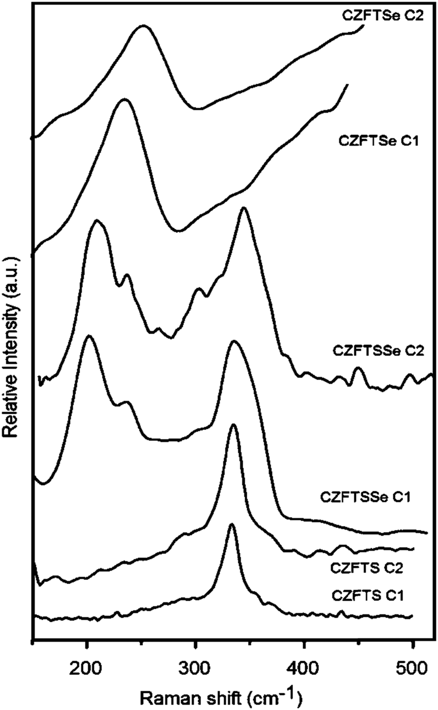 | ||
| Fig. 8 Raman spectra of Zn-rich and Fe-rich (C2CZFTS (CZFTS C1 and CZFTS C2), CZFTSe (CZFTSe C1 and CZFTSe C2) and CZFTSSe (CZFTSSe C1 and CZFTSSe C2) thin films deposited at 350 °C using different precursor mixtures. | ||
Raman spectra for the CZFTSSe films showed peaks at ∼198, 228 and ∼340 cm−1. All these peaks are shifted from Raman peaks for CFTSe (209, 270 cm−1) or CFTS (321, 284, 218 cm−1) phases as expected.7,8,26–28 Band gap measurements of CZFTS for Zn-rich composition showed 1.72 eV whereas those with Fe-rich composition gave a band gap of 1.67 eV, which are close to those reported previously.2,7 Raman spectra obtained for the Fe-rich CZFTSe films showed a broad peak with low intensity at 230 cm−1. The Zn-rich CZFTSe Raman shifts were observed at ∼235 cm−1 which lies between the end materials CZTSe and CFTSe phases with their corresponding Raman modes at 209 cm−1 and 270 cm−1 respectively.27
Here also the Zn-rich phases showed slightly higher Raman mode as observed in CZFTS.2,7 The calculated band gaps were 1.48 and 1.47 eV for Zn-rich and Fe-rich CZFTSe thin films respectively which are in the range of CZTS, CZTSe, CZTSSe and CFTSe.27–29 UV/Vis Tauc plots drawn by ploting (αhν)2 against hν gave a band gap values of ∼1.64 and 1.61 eV for Zn-rich and Fe-rich CZFTSSe thin films, which were closer to that of the Kesterite CZFTS phases.2,6–8,14–20
Electrical sheet resistance
Variation in the electrical sheet resistance with different Fe-compositions has been studied. The electrical resistance measured at room temperature were 2.48 KΩ sq−1 for Fe-rich thin films and 2.42 KΩ sq−1 for Zn-rich films of CZFTS values which lie between the electrical sheet resistance for parent materials CZTS (2.8 KΩ sq−1) and CFTS (2.3 KΩ sq−1).9,28–31 The Fe-rich films showed comparatively lower resistance than the Zn-rich ones. The sheet resistance of the Zn-rich CZFTSe films and Fe-rich phases were observed as 2.10 KΩ sq−1 for and 2.07 KΩ sq−1 respectively, both values were lower than those for CZFTS (2.48 KΩ sq−1 and 2.42 KΩ sq−1) as expected.The resistance value for end materials were as CZTSe (2.12 KΩ sq−1) and CFTSe (2.04 KΩ sq−1). These resistance measurements for CZFTSSe materials were found to be 2.31 and 2.29 KΩ sq−1 for Zn-rich and Fe-rich films respectively. Both values are lower than those of CZFTS Fe-rich (2.48 KΩ sq−1) and Zn-rich phases (2.42 KΩ sq−1) but higher than the CZFTSe Zn-rich (2.10 KΩ sq−1) and Fe-rich (2.07 KΩ sq−1) phases32,33 (ESI,† Fig. S4).
Vegard-type analysis were carried out using the measured band gap and sheet resistance values and is shown in Fig. 9. There is a reasonable linear correlation between the Se/S mole fraction in all samples and these properties for all the films.
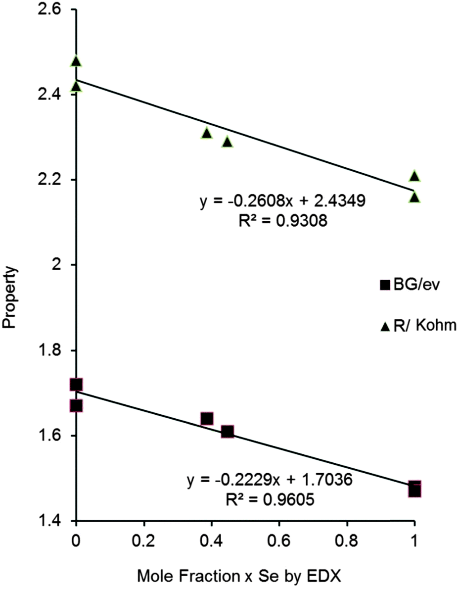 | ||
| Fig. 9 Vegard-type plot for resistance and band gaps of all samples against the mole fraction of Se as measured by EDX (band gap eV, resistance KΩ sq−1). | ||
Conclusions
Thin films of CZFTS, CZFTSe and CZFTSSe have been deposited by AACVD. The ratios of the constituents: Zn, Fe, S and Se can be controlled by varying the concentrations of corresponding precursors and the deposition temperature. The band gaps of these materials lie between 1.0 eV and 1.7 eV on changing the [Zn]:[Fe] and [S]:[Se] ratios in the material. These band gaps are ideal for absorber material in thin film solar cells. The sheet resistance of the materials are good for polycrystalline CZTS PV-cells. The structural parameters for the films do not show any consistent variation with composition, and given the wide range of differing radii of the ions involved this observation is perhaps not surprising. There is a distinct irregular trend following the mole fraction of selenium (Table 1). The band gap and resistance of each film is overwhelmingly controlled by the selenium content as shown in Fig. 8. Dhurba and Kim have demonstrated the potential of such materials for solar cells.7 We now present a viable CVD method for their deposition. The potential for the use of these materials in devices will be investigated in the future.
Acknowledgements
We thank EPSRC for funding instruments, under grant number EP/K039547/1), used for characterization of compounds. PK thanks the School of Chemistry, The University of Manchester for funding.Notes and references
- D. B. Mitzi, O. Gunawan, T. K. Todorov, K. Wang and S. Guha, Sol. Energy Mater. Sol. Cells, 2011, 95, 1421–1436 CrossRef CAS PubMed.
- G. L. Agawane, S. W. Shin, S. A. Vanalakar, A. V. Moholkar and J. H. Kim, Mater. Lett., 2014, 137, 147–149 CrossRef CAS PubMed.
- X. Fontane, V. Izquierdo-Roca, E. Saucedo, S. Schorr, V. O. Yukhymchuk and M. Y. Valakh, J. Alloys Compd., 2012, 539, 190–194 CrossRef CAS PubMed.
- P. Bonazzi, L. Bindi, G. P. Bernardini and S. Menchetti, Can. Mineral., 2003, 41, 639 CrossRef CAS.
- T. Shibuya, Y. Goto, Y. Kamihara, M. Matoba, K. Yasuoka, L. A. Burton and A. Walsh, Appl. Phys. Lett., 2014, 104, 021912 CrossRef PubMed.
- S. R. Hall, J. T. Szymanski and J. M. Stewart, Can. Mineral., 1978, 16, 131–137 CAS.
- D. B. Khadka and J. J. Kim, J. Phys. Chem. C, 2014, 118, 14227 CAS.
- S. H. Chang, M. Y. Chiang, C. C. Chiang, F. W. Yuan, C. Y. Chen, B. C. Chiu, T. L. Kao, C. H. Lai and H. Y. Tuan, Energy Environ. Sci., 2011, 4, 4929–4932 CAS.
- (a) P. Marchand, I. A. Hassan, I. P. Parkin and C. J. Carmalt, Dalton Trans., 2013, 42, 9406–9422 RSC; (b) M. Nyman, M. J. Hampden-Smith and E. A. Duesler, Chem. Vap. Deposition, 1996, 2, 171–173 CrossRef CAS PubMed.
- M. N. McCain, S. Schneider, M. R. Salata and T. J. Marks, Inorg. Chem., 2008, 47, 2534–2542 CrossRef CAS PubMed.
- (a) C. R. Crick and I. P. Parkin, J. Mater. Chem., 2009, 19, 1074–1076 RSC; (b) M. R. Waugh, G. Hyett and I. P. Parkin, Chem. Vap. Deposition, 2008, 14, 366–372 CrossRef CAS PubMed.
- K. G. U. Wijayantha, S. Saremi-Yarahmadia and L. M. Peter, Phys. Chem. Chem. Phys., 2011, 13, 5264–5270 RSC.
- A. Tahir, M. Mazhar, M. Hamid, K. G. U. Wijayantha and K. C. Molloy, Dalton Trans., 2009, 3674–3680 RSC.
- A. Tahir, K. G. U. Wijayantha, S. Saremi-Yarahmadi, M. Mazhar and V. McKee, Chem. Mater., 2009, 21, 3763–3772 CrossRef CAS.
- (a) K. Ramasamy, V. L. Kuznetsov, K. Gopal, M. A. Malik, J. Raftery, P. Edwards and P. O'Brien, Chem. Mater., 2013, 25, 266K–276K CrossRef; (b) P. Kevin, D. J. Lewis, J. Raftery, M. A. Malik and P. O'Brien, J. Cryst. Growth, 2015, 415, 93–99 CrossRef CAS PubMed.
- K. Ramasamy, M. A. Malik and P. O'Brien, Chem. Sci., 2011, 2, 1170 RSC.
- S. Mahboob, S. N. Malik, N. Haider, C. Q. Nguyen, M. A. Malik and P. O'Brien, J. Cryst. Growth, 2014, 394, 39 CrossRef CAS PubMed.
- A. Adeogun, M. Afzaal and P. O'Brien, Chem. Vap. Deposition, 2006, 12, 597–599 CrossRef CAS PubMed.
- (a) D. J. Lewis and P. O'Brien, Chem. Commun., 2014, 50, 6319 RSC; (b) P. Kevin, S. N. Malik, M. A. Malik and P. O'Brien, Chem. Commun., 2014, 50, 14328–14330 RSC.
- R. A. Hussain, A. Badshah, M. Dilshad Khan, N. Haider, B. Lal, S. Ishtiaq Khan and A. Shah, Mater. Chem. Phys., 2015, 159, 152–158 CrossRef CAS PubMed.
- P. Brack, J. S. Sagu, T. A. N. Peiris, A. McInnes, M. Senili, K. G. U. Wijayantha, F. Marken and E. Selli, Chem. Vap. Deposition, 2015, 21, 41–45 CrossRef CAS PubMed.
- M. A. Ehsan, T. A. Nirmal Peiris, K. G. Upul Wijayantha, M. M. Olmstead, Z. Arifin, M. Mazhar, K. M. Loa and V. McKeeb, Dalton Trans., 2013, 42, 10919–10928 RSC.
- N. Revaprasadu, M. A. Malik and P. O'Brien, J. Mater. Res., 1999, 14, 3237 CrossRef CAS; M. A. Malik, M. Motevalli and P. O'Brien, Inorg. Chem., 1995, 34, 6223 CrossRef; M. A. Malik, M. Motevalli, P. O'Brien and J. R. Walsh, Organometallics, 1992, 11, 3136 CrossRef; A. A. M. Memon, M. Afzaal, M. A. Malik, C. Nguyen, P. O'Brien and J. Raftery, Dalton Trans., 2006, 4499 RSC; D. J. Binks, S. P. Bants, D. P. West, M. A. Malik and P. O'Brien, J. Mod. Opt., 2003, 50, 299 Search PubMed; C. Q. Nguyen, A. E. Adeogun, M. Afzaal, M. A. Malik and P. L. O'Brien, Chem. Commun., 2006, 2182 RSC; M. A. Malik, M. Motevalli, T. Saeed and P. O'Brien, Adv. Mater., 1993, 5, 653 CrossRef PubMed; A. Panneerselvam, C. Q. Nguyen, M. A. Malik, P. O'Brien and J. Raftery, J. Mater. Chem., 2009, 19, 419–427 RSC; N. Revaprasadu, M. A. Malik and P. O'Brien, S. Afr. J. Chem., 2004, 57, 40–43 Search PubMed.
- M. Akhtar, J. Akhter, M. A. Malik, P. O'Brien, F. Tuna, J. Raftery and M. Helliwell, J. Mater. Chem., 2011, 21, 9737–9745 RSC.
- M. B. Hursthouse, M. A. Malik, M. Motevalli and M. P. O'Brien, J. Mater. Chem., 1992, 2, 949 RSC.
- E. S. Schorr, V. O. Yukhymchuk, M. Y. Valakh, A. Pérez-Rodríguez and J. R. Morante, J. Alloys Compd., 2012, 539, 190–194 CrossRef PubMed.
- M. Cao, B. L. Zhang, J. Huang, Y. Sun, L. J. Wang and Y. Shen, Chem. Phys. Lett., 2014, 604, 15–21 CrossRef CAS PubMed.
- S. C. Riha, B. A. Parkinson and A. L. Prieto, J. Am. Chem. Soc., 2011, 133, 15272–15275 CrossRef CAS PubMed.
- C. Jiang, J. S. Lee and D. V. Talapin, J. Am. Chem. Soc., 2012, 134, 5010–5013 CrossRef CAS PubMed.
- X. Zhang, N. Bao, K. Ramasamy, Y. H. A. Wang, Y. Wang, B. Lin and A. Gupta, Chem. Commun., 2012, 48, 4956 RSC.
- H. Katagiri, K. Saitoh, T. Washio, H. Shinohara, T. Kurumadani and S. Miyajima, Sol. Energy Mater. Sol. Cells, 2001, 65, 141–148 CrossRef CAS.
- X. Yu, A. Ren, F. Wang, C. Wang, J. Zhang, W. Wang, L. Wu, W. Li, G. Zeng and L. Feng, Int. J. Photoenergy, 2014, 6, 1–9 Search PubMed.
- E. M. Mkawi, K. Ibrahim, M. K. M. Ali and A. S. Mohamed, Int. J. Electrochem. Sci., 2013, 8, 359–368 CAS.
Footnote |
| † Electronic supplementary information (ESI) available. See DOI: 10.1039/c5tc00867k |
| This journal is © The Royal Society of Chemistry 2015 |