
 Open Access Article
 This Open Access Article is licensed under a Creative Commons Attribution-Non Commercial 3.0 Unported Licence
Stability and electronic properties of silicene on WSe2
Jiajie
Zhu
and
Udo
Schwingenschlögl
*
PSE Division, King Abdullah University of Science and Technology, Thuwal 23955-6900, Kingdom of Saudi Arabia. E-mail: udo.schwingenschlogl@kaust.edu.sa
First published on 17th March 2015
Abstract
Many semiconducting substrates, such as GaS and MgBr2, have been explored for silicene. However, large lattice mismatches, complicated control of terminal layers and small band gaps are critical limiting factors. First-principles results on the stability and electronic properties of silicene on WSe2 show that the energy barriers for lateral translation between the two subsystems are very small due to weak van der Waals interactions. For the same reason, the Dirac physics of silicene is preserved. It turns out that the induced band gap is sufficient to withstand thermal fluctuations.
1 Introduction
Silicene, first proposed theoretically by Takeda and Shiraishi in 1994,1 consists of a monolayer of Si atoms in a two-dimensional honeycomb structure, just like graphene. Even though freestanding silicene is subject to buckling (sp2–sp3 hybridization),2,3 the Dirac cone at the corner of the Brillouin zone (linearly dispersing π and π* bands) is maintained.4 In addition to its electronic similarity to graphene,5–7 silicene is also suitable to be integrated in current Si-based nanoelectronics. Furthermore, the stronger spin–orbit coupling as compared to graphene opens new avenues for applications.8Although silicene has been successfully deposited on several metallic substrates, including ZrB2(0001),9 Ir(111)10 and Ag(111),11,12 the Dirac characteristics are destroyed because of hybridization of π bands with the substrate.13–15 On the other hand, semiconducting substrates have been investigated in order to avoid such strong interaction. For example, GaS nanosheets have been predicted to yield a Dirac cone with a 170 meV band gap, while the lattice mismatch of 7.5% casts doubts on the stability of this hybrid system.16 Kokott and coworkers have found for silicene on H(Cl)-passivated Si(111) substrate (lattice mismatch less than 1%) linearly dispersing π bands with a band gap of 3(56) meV.17,18 Similar results have been reported for H-passivated Si- and C-terminated SiC(0001).19,20 Although Dirac physics can be achieved on MgX2(0001) (X = Cl, Br and I) substrates without dangling surface bonds, which simplifies the synthesis, band gaps below 16 meV strongly limit the applicability.21 A band gap of 52 meV is induced by F-terminated CaF2(111), but control of the preparation process is very problematic.18
A band gap of some 100 meV is typically desirable to overcome thermal fluctuations at room temperature. Several approaches have been studied to open such a band gap in graphene, including external electric fields22,23 and multilayer stacking,24,25 which may also be useful for silicene. However, the experimentally accessible electric fields limit the band gap to about 30 meV.26,27 Moreover, adjacent Si layers are predicted to form clusters instead of bilayer silicene, which completely destroys any Dirac states because of the strong interaction.21,28 While adsorbed metal atoms are predicted to open a band gap in freestanding silicene, they may aggregate instead of maintaining a uniform distribution.29,30 WSe2 is a semiconductor with a hexagonal structure consisting of sandwich-like layers along the [001] direction without dangling bonds.31 It has minimal lattice mismatch with low-buckled silicene among the transition metal dichalcogenides, consequently overcoming the practical obstacles caused by related substrates with much larger lattice mismatch.32 Since the van der Waals interaction is expected to be stronger than for MgBr2 (more electrons are contributing to the dipole), the band gap of silicene on WSe2 is expected to be enhanced. Therefore, WSe2 appears to fulfill all criteria of a suitable substrate for silicene. We will investigate in this work the stability and electronic properties of this hybrid system and will demonstrate very encouraging results.
2 Computational method
Electronic structure calculations are performed in the framework of density functional theory and the projector augmented wave method.33 The generalized gradient approximation of Perdew, Burke and Ernzerhof is employed for the exchange–correlation potential34 and the long-range van der Waals interaction is taken into account by the DFT-D2 method.35 The cut-off energy for the plane wave basis is set to 400 eV and an energy tolerance of 10−6 eV is selected for the iterative solution of the Kohn–Sham equations. Brillouin zone integrations are performed with 9 × 9 × 1 k-meshes in the structure optimizations and 18 × 18 × 1 k-meshes in the electronic structure calculations. All structures are relaxed until the residual forces on the atoms have declined to less than 0.01 eV Å−1.The in-plane lattice constant of WSe2(001) is found to be 3.313 Å and thus similar to the experimental and previous theoretical values of 3.282 Å and 3.31 Å, respectively.36 The lattice mismatch between 2 × 2 WSe2 and 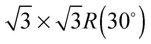 low-buckled silicene is only 0.6%. High-buckled silicene is also considered, since it has been prepared on MoS2.37 Furthermore, monolayer WSe2 has been obtained by mechanical exfoliation.38 We use a vacuum layer of 15 Å thickness to avoid unphysical interaction between images due to the periodic boundary conditions. Dipole corrections result only in tiny energy variations of less than 0.1 meV per atom. Low-buckled silicene on bilayer WSe2 is investigated for comparison with the monolayer case. In addition, S and Te atoms are substituted for Se (concentration 12.5%) to modify the stability of the hybrid system as well as the band gap of silicene.
3 Results and discussion
Fig. 1(a) shows the structure of low-buckled silicene on monolayer WSe2, where the W and Se atoms are located on top of the hollow and bridge sites of the Si hexagons (which we will call in the following the unshifted structure). According to the structural parameters summarized in Table 1, the buckling height of the Si atoms (0.51 Å) as well as the binding energy (122 meV) are larger than in the case of the MgBr2 substrate (0.49 Å and 63 meV) due to the stronger van der Waals interaction.21 Moveover, the binding energy is close to that of low-buckled silicene on MoS2 (120 meV).39 A bilayer WSe2 substrate yields little differences for the structural properties of silicene. The Si buckling height and in-plane lattice constant are virtually identical to the monolayer result, whereas the distance between the substrate and silicene grows by about 1% to 3.23 Å. Since the binding energy (121 meV) is also similar, we conclude that already the WSe2 monolayer accurately models realistic substrate thicknesses.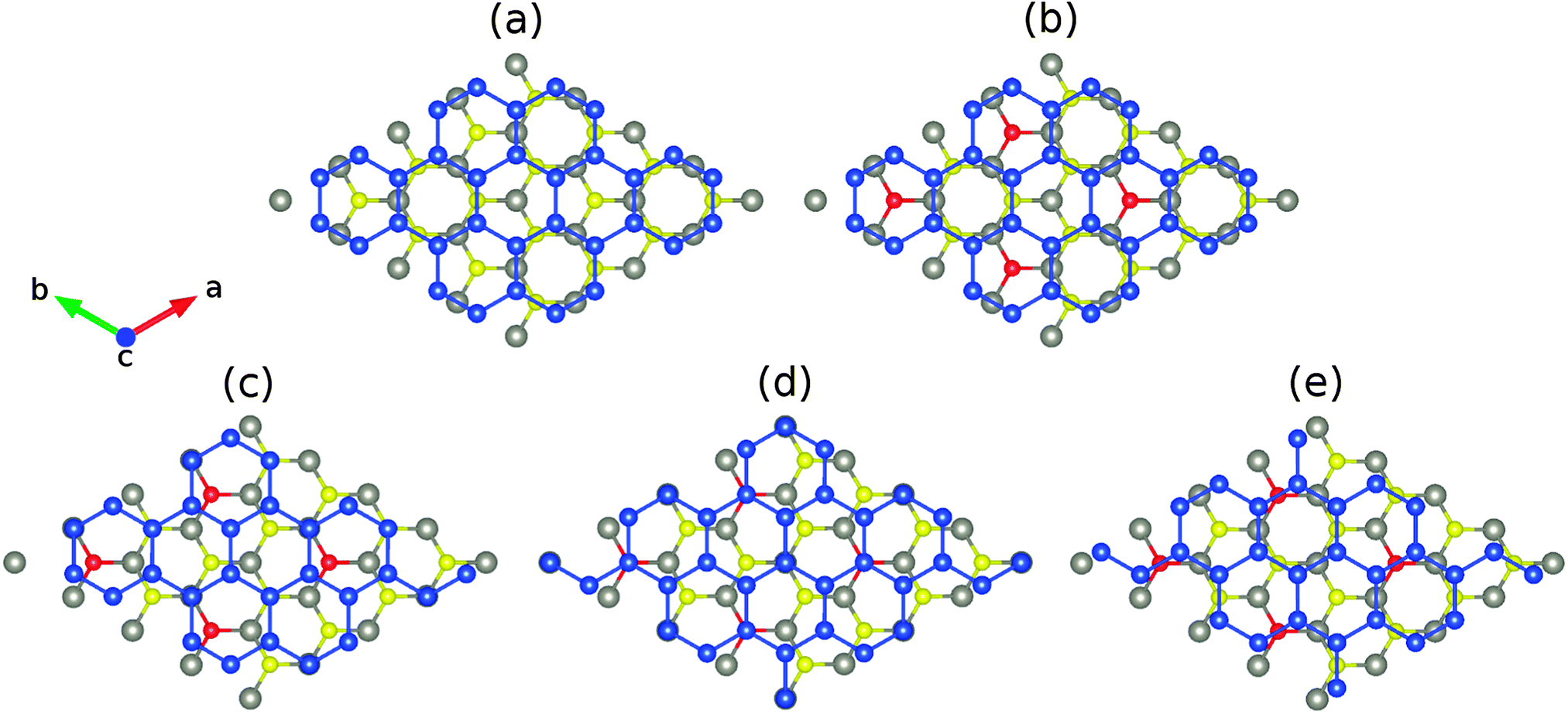 | ||
| Fig. 1 Top view of low-buckled silicene on (a) undoped WSe2 without lateral shift and (b–e) S/Te doped WSe2 with lateral shifts of 0, 1/6, 1/3 and 1/2 along the [100] direction. The W, Se, Si and S/Te atoms are shown in gray, yellow, blue and red color. | ||
| S doping | Pristine | Te doping | |
|---|---|---|---|
| b sil (Å) | 0.51 | 0.51 | 0.49 |
| d sil-sub (Å) | 3.19 | 3.20 | 3.03 |
| a (Å) | 3.829 | 3.842 | 3.861 |
| E (meV) | 112 | 122 | 135 |
| ΔH (eV) | 0.01 | 0.32 | |
| d W-dop (Å) | 2.42 | 2.54 | 2.73 |
The variation of the total energy of the hybrid system as a function of the lateral shift along the [100] direction with respect to the unshifted structure is illustrated in Fig. 2. Note that the [100] and [010] directions are equivalent due to the three-fold rotational symmetry of the lattice. The unshifted structure in addition has mirror symmetry and the translational periodicity is half of the cell size due to the 2 × 2 WSe2 supercell. The maximal translation energy barrier is found to be less than 0.4 meV per atom, which reflects a high uncertainty in the structure of the hybrid system at room temperature as well as below. The binding energy of the two components is also addressed in Fig. 2, showing a variation of less than 2 meV per Si atom with distinct valleys at lateral shifts of ±0.25 along the [100] direction.
 | ||
| Fig. 2 Total energy per atom with respect to the unshifted structure and binding energy per Si atom for low-buckled silicene on WSe2 as a function of the lateral shift along the [100] direction. | ||
We next substitute S or Te for Se to modify the interaction at the interface, see Fig. 1. Different configurations of the dopant atoms ranging from clusters to a homogeneous distribution are compared. The latter turns out to be energetically favorable due to small local distortions around the dopant atoms, which are located on top of the Si atoms for 1/6 and 1/3 lateral shifts, respectively, and occupy hollow and bridge sites for 0 and 1/2 lateral shifts. The corresponding formation energies are 0.01 and 0.32 eV (Table 1). The W–S (2.42 Å) and W–Te (2.73 Å) bond lengths deviate from the W–Se bond length (2.54 Å) as expected from the ionic radii (1.70, 1.84 and 2.07 Å for S, Se and Te, respectively). Smaller (3.829 Å) and larger (3.861 Å) in-plane lattice constants are predicted for S and Te doping. In addition, the distance between silicene and the substrate remaines similar for S doping (3.19 Å) but is significantly reduced for Te doping (3.03 Å), see Table 1. For S doping a ±1/3 lateral shift is energetically favorable, see Fig. 2, whereas the unshifted structure now has the highest total energy. The resistance against translation is enhanced substantially as compared to the pristine case, which is a consequence of stronger variations of the binding energy. Under Te doping the unshifted structure is most stable and the maximal translation energy barrier is enhanced to 7 meV, which corresponds to a binding energy difference of 19 meV per Si atom (including 2 meV of relaxation energy from the substrate).
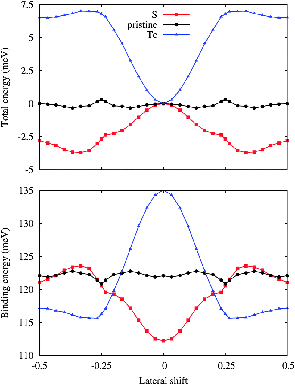
Fig. 3 shows densities of states without shift and with a lateral shift of 1/3 (most and least stable configurations for different dopings). The top of the valence band and the bottom of the conduction band are dominated by Si 3p states. Hybridization between the substrate and Si 3p states extends closer to the valence band maximum for Te doping than for S doping due to the smaller distance to the silicene. Moreover, larger hybridizations between the S/Te p and Si 3p states are characteristic for the unshifted structures. The band structures in Fig. 4 show the Dirac cone, as expected, at the Γ point. While alkali metal intercalation can also restore the Dirac cone of double-layered silicene, the present system is less difficult to handle experimentally.40 Without lateral shift we obtain band gaps of 0.30, 0.32 and 0.34 eV for S doped, pristine and Te doped WSe2. The slight increase reflects the growing interaction at the interface, compare Table 1. Spin–orbit coupling reduces the band gap of the pristine system without lateral shift by 2.8 meV due to spin splitting (2.0 meV in the valence band and 1.5 meV in the conduction band), which is negligible as compared to the original value. On the other hand, the band gap is close to zero for the shifted structures because of weaker interaction: in the unshifted case S/Se/Te occupies a hollow site and thus has six Si neighbours, whereas in the shifted case it occupies a top site with only a single interaction partner. Although Se vacancies are inevitable in monolayer WSe2,41 they only slightly reduce the band gap, for example by 0.06 eV for undoped WSe2 without lateral shift (one Se vacancy in a 4 × 4 supercell), and leave the principal features of the band structure unaffected.
 | ||
| Fig. 3 Density of states of low-buckled silicene on (a, b) S doped, (c, d) pristine and (e, f) Te doped WSe2 without lateral shift (left row) and with a 1/3 lateral shift (right row). | ||
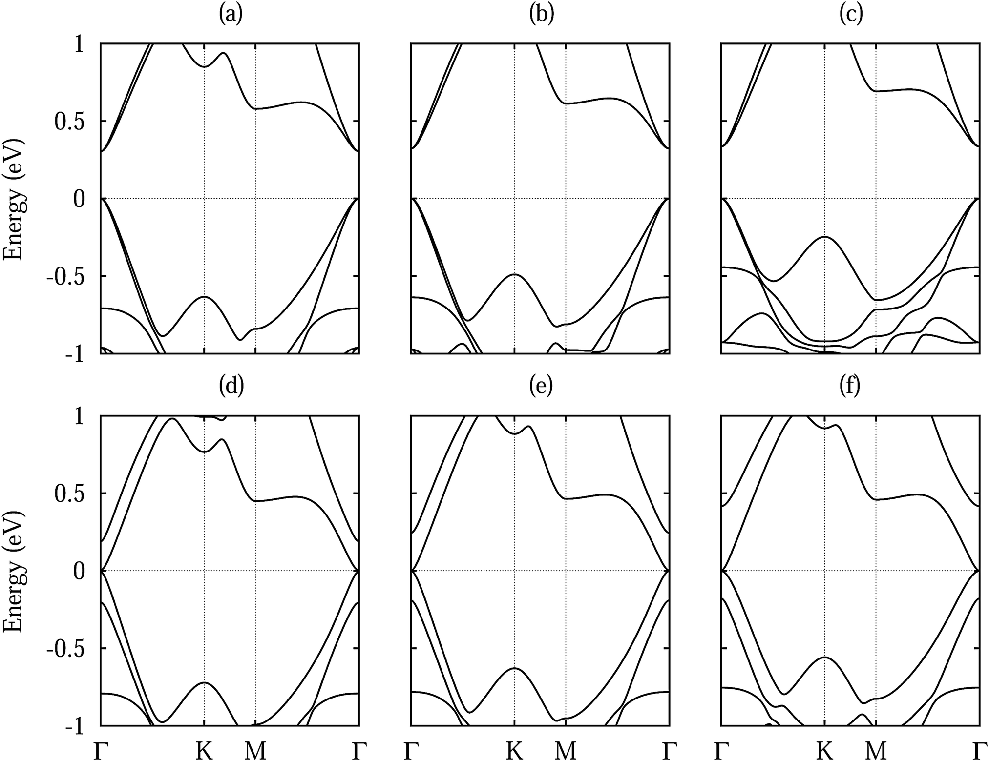 | ||
| Fig. 4 Band structure of low-buckled silicene on (a, d) S doped, (b, e) pristine and (c, f) Te doped WSe2 without lateral shift (upper row) and with a 1/3 lateral shift (lower row). | ||
The position of the Dirac point (middle point between the π and π* bands) with respect to the Fermi level and the corresponding band gap are illustrated in Fig. 5. Doping is found to have hardly any effect on both these quantities. On the other hand, the band gaps are reduced to almost zero for the 1/6 and 1/3 lateral shifts, which are structurally similar with the W and Se or dopant atoms on top of the Si atoms. Since the translation energy barrier is quite small for the pristine substrate, thermal fluctations even at low temperature can modify the electronic properties dramatically, ranging from metallic to semiconducting characters. On the contrary, stable metallic and semiconducting silicene is obtained by S and Te doping, respectively. In each case the Dirac point is located less than 0.16 eV above the Fermi level, reflecting weakly p-doped silicene. The position of the Dirac point follows the same trend as the band gap, which suggests that the value of the band gap is determined by the amount of charge redistribution between silicene and substrate. Indeed, the internal electric field created at the interface breaks the symmetry of the two silicene sublattices, which opens the band gap.
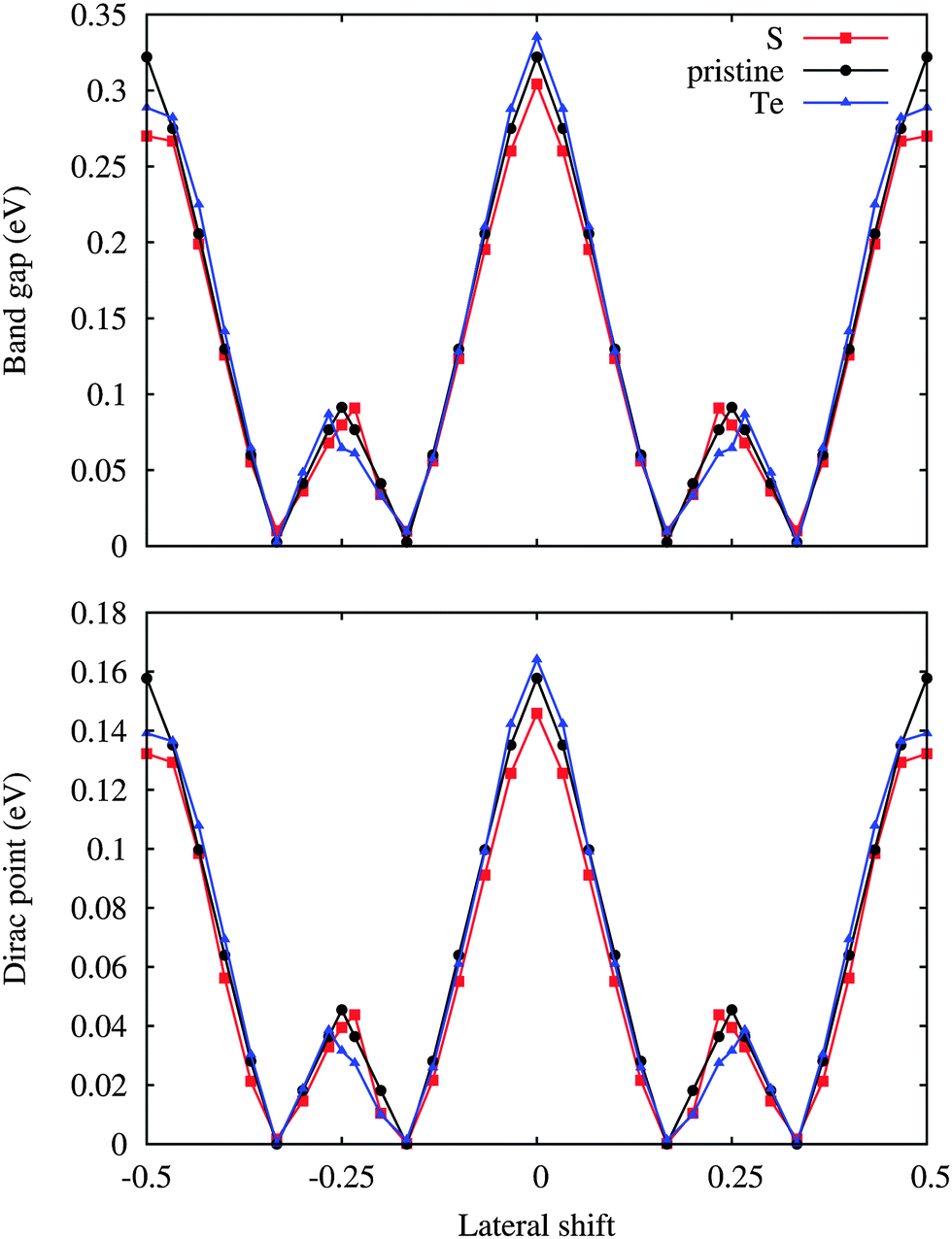 | ||
| Fig. 5 Position of the Dirac point with respect to the Fermi level and band gap as a function of the lateral shift along the [100] direction for low-buckled silicene. | ||
The charge density difference Δρ = ρhyb + ρsil + ρsub (ρhyb, ρsil and ρsub being the charge densities of the hybrid system, silicene and substrate, respectively) due to interaction of silicene with WSe2 is shown in Fig. 6 for the cases without and with a lateral 1/3 shift. Both ρsil and ρsub are calculated with the same parameters as ρhyb. From left to right Fig. 6 shows an enhanced charge density redistribution at the interface of the two subsystems for the unshifted structure (upper row), reflecting the growing interaction (the number of valence electrons grows along the series S–Se–Te). Charge also shifts within the silicene sheet from the lower sublattice to the upper sublattice. Under the lateral shift (lower row) the charge density redistribution at the interface is substantially weaker.
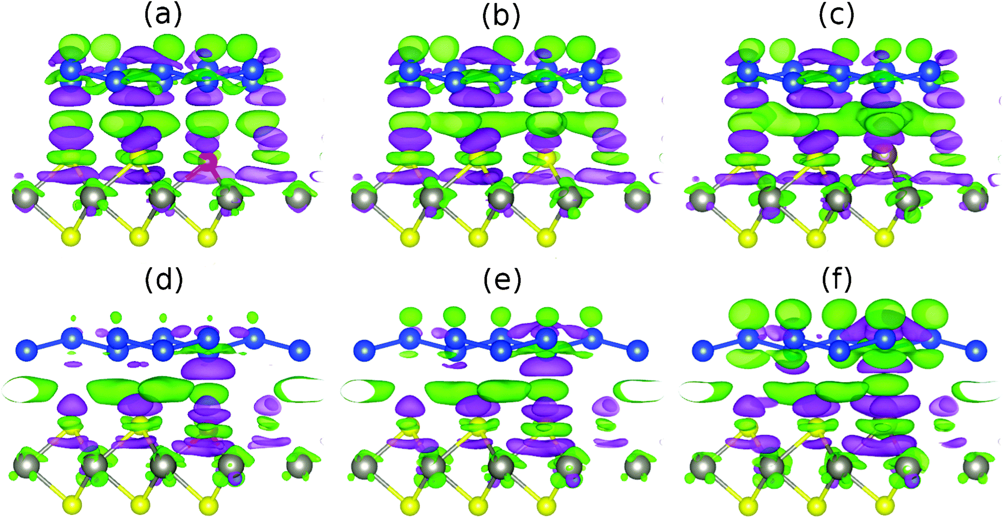 | ||
| Fig. 6 Charge density difference due to the interaction of low-buckled silicene with (a, d) S doped, (b, e) pristine and (c, f) Te doped WSe2 without lateral shift (upper row) and with a 1/3 shift (lower row). Green (purple) color represents charge accumulation (depletion), where the isosurfaces refer to isovalues of 3 × 10⁻⁴ electrons per bohr3. The W, Se, Si, S and Te atoms are shown in gray, yellow, blue, red and brown color. | ||
The structure of high-buckled silicene on WSe2 is shown in Fig. 7 for different locations of the Si atoms, namely on top of W, Se and the hollow site. The first case turns out to be energetically favorable by 10 and 3 meV per atom with respect to the other cases, respectively. The Si buckling height is found to be 1.3 Å, which is smaller than in the case of high-buckled silicene on the MoS2 substrate (2.0 Å) due to a reduced lattice compression.37 The larger binding energy (195 meV) as compared to low-buckled silicene (122 meV) is a consequence of the smaller distance to the substrate (2.55 Å instead of 3.20 Å). This strong interaction destroys the Dirac cone, see Fig. 7(d), in contrast to the low-buckled system and similar to previous results on the MoS2 substrate.37,42
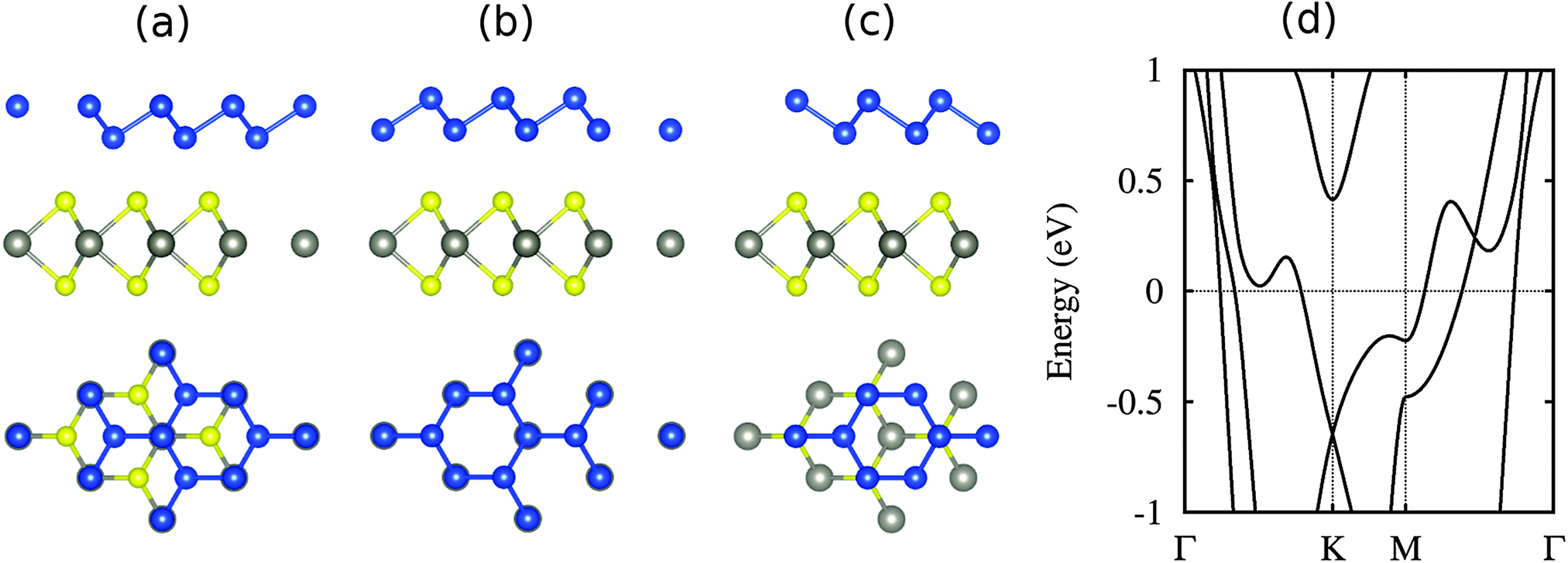 | ||
| Fig. 7 (a–c) Side and top views of high-buckled silicene on WSe2 for different configurations, see the text for details. The W, Se and Si atoms are shown in gray, yellow and blue color. (d) Band structure of the lowest energy configuration (a). | ||
4 Conclusions
The stability and electronic properties of silicene on the semiconducting WSe2 substrate have been investigated using first-principles calculations, motivated by the minimal lattice mismatch. The undoped substrate suffers from the structural uncertainty coming from the possibility of lateral shifts between the component systems due to small translation energy barriers. Therefore, electronic structures ranging from metallic to semiconducting silicene are encountered and can fluctuate even at low temperature. On the other hand, silicene on S and Te doped WSe2 turns out to be stable metallic and semiconducting, respectively, because of different interaction strengths. The translation energy barrier and binding energy for Te doping amount to 7 meV and 135 meV, respectively. The Dirac physics of silicene is preserved with the Dirac point located 160 meV above the Fermi level due to charge redistribution. A band gap of 340 meV is achieved, which withstands thermal fluctuations at room and elevated temperatures and results in an improved applicability of the proposed hybrid system.Using WSe2 as a support will open access to the unique properties of silicene, which so far could not be utilized as they were always perturbed by the substrate. Of particular interest are the unusual performances of silicene-based spintronic devices8 and the potential to obtain ultra high speed (THz frequency range) field-effect transistors. Such field-effect transistors show a high on/off current ratio43 but require a complicated preparation procedure.44 All this is only possible if the fundamental shortcomings of the current substrates are resolved. On the one hand, the Dirac cone has to be preserved, which excludes many potential candidates. On the other hand, the lattice mismatch has to be small to avoid strain effects on silicene, the termination must not cause complications, and the band gap must be intrinsically large enough to operate at standard temperatures. All these criteria can be achieved by utilizing WSe2 to exploit the intrinsic properties of silicene, thus avoiding, for example, the large supply voltage required when adatoms are used to open the band gap.45 It should be noted that silicene already has been grown epitaxially on MoS2,37 which is isostructural to WSe2 and has very similar physical and chemical properties, so that the same preparation method can be expected to be successful.
Acknowledgements
Research reported in this publication was supported by the King Abdullah University of Science and Technology (KAUST).References
- K. Takeda and K. Shiraishi, Theoretical Possibility of Stage Corrugation in Si and Ge Analogs of Graphite, Phys. Rev. B: Condens. Matter Mater. Phys., 1994, 50, 14916–14922 CrossRef CAS.
- E. Durgun, S. Tongay and S. Ciraci, Silicon and III-V Compound Nanotubes: Structural and Electronic Properties, Phys. Rev. B: Condens. Matter Mater. Phys., 2005, 72, 075420 CrossRef.
- N. J. Roome and J. D. Carey, Beyond Graphene: Stable Elemental Monolayers of Silicene and Germanene, ACS Appl. Mater. Interfaces, 2014, 6, 7743–7750 CAS.
- S. Cahangirov, M. Topsakal, E. Aktürk, H. Şahin and S. Ciraci, Two- and One-Dimensional Honeycomb Structures of Silicon and Germanium, Phys. Rev. Lett., 2009, 102, 236804 CrossRef CAS.
- K. S. Novoselov, A. K. Geim, S. V. Morozov, D. Jiang, Y. Zhang, S. V. Dubonos, I. V. Grigorieva and A. A. Firsov, Electric Field Effect in Atomically Thin Carbon Films, Science, 2004, 306, 666–669 CrossRef CAS PubMed.
- A. H. Castro Neto, F. Guinea, N. M. R. Peres, K. S. Novoselov and A. K. Geim, The Electronic Properties of Graphene, Rev. Mod. Phys., 2009, 81, 109–162 CrossRef CAS.
- K. S. Novoselov, V. I. Fal'ko, L. Colombo, P. R. Gellert, M. G. Schwab and K. Kim, A Roadmap for Graphene, Nature, 2012, 490, 192–200 CrossRef CAS PubMed.
- C. Liu, W. Feng and Y. Yao, Quantum Spin Hall Effect in Silicene and Two-Dimensional Germanium, Phys. Rev. Lett., 2011, 107, 076802 CrossRef.
- A. Fleurence, R. Friedlein, T. Ozaki, H. Kawai, Y. Wang and Y. Yamada-Takamura, Experimental Evidence for Epitaxial Silicene on Diboride Thin Films, Phys. Rev. Lett., 2012, 108, 245501 CrossRef.
- L. Meng, Y. Wang, L. Zhang, S. Du, R. Wu, L. Li, Y. Zhang, G. Li, H. Zhou, W. A. Hofer and H. Gao, Buckled Silicene Formation on Ir(111), Nano Lett., 2013, 13, 685–690 CrossRef CAS PubMed.
- P. Vogt, P. De Padova, C. Quaresima, J. Avila, E. Frantzeskakis, M. C. Asensio, A. Resta, B. Ealet and G. Le Lay, Silicene: Compelling Experimental Evidence for Graphene like Two-Dimensional Silicon, Phys. Rev. Lett., 2012, 108, 155501 CrossRef.
- D. Tsoutsou, E. Xenogiannopoulou, E. Golias, P. Tsipas and A. Dimoulas, Evidence for Hybrid Surface Metallic Band in (4 × 4) Silicene on Ag(111), Appl. Phys. Lett., 2013, 103, 231604 CrossRef PubMed.
- D. Kaltsas, L. Tsetseris and A. Dimoulas, Structural Evolution of Single-Layer Films during Deposition of Silicon on Silver: A First-Principles Study, J. Phys.: Condens. Matter, 2012, 24, 442001 CrossRef CAS PubMed.
- C.-L. Lin, R. Arafune, K. Kawahara, M. Kanno, N. Tsukahara, E. Minamitani, Y. Kim, M. Kawai and N. Takagi, Substrate-Induced Symmetry Breaking in Silicene, Phys. Rev. Lett., 2013, 110, 076801 CrossRef.
- Y. Wang and H. Cheng, Absence of a Dirac Cone in Silicene on Ag(111): First-Principles Density Functional Calculations with a Modified Effective Band Structure Technique, Phys. Rev. B: Condens. Matter Mater. Phys., 2013, 87, 245430 CrossRef.
- Y. Ding and Y. Wang, Electronic Structures of Silicene/GaS Heterosheets, Appl. Phys. Lett., 2013, 103, 043114 CrossRef PubMed.
- S. Kokott, L. Matthes and F. Bechstedt, Silicene on Hydrogen-Passivated Si(111) and Ge(111) Substrates, Phys. Status Solidi RRL, 2013, 7, 538–541 CrossRef CAS.
- S. Kokott, P. Pugradt, L. Matthes and F. Bechstedt, Nonmetallic Substrates for Growth of Silicene: An Ab Initio Prediction, J. Phys.: Condens. Matter, 2014, 26, 185002 CrossRef CAS PubMed.
- N. Gao, J. Li and Q. Jiang, Bandgap Opening in Silicene: Effect of Substrates, Chem. Phys. Lett., 2014, 592, 222–226 CrossRef CAS PubMed.
- H. Liu, J. Gao and J. Zhao, Silicene on Substrates: A Way to Preserve or Tune Its Electronic Properties, J. Phys. Chem. C, 2013, 117, 10353–10359 CAS.
- J. Zhu and U. Schwingenschlögl, Structural and Electronic Properties of Silicene on MgX2 (X = Cl, Br, and I), ACS Appl. Mater. Interfaces, 2014, 6, 11675–11681 CAS.
- L. Huang, Q. Yue, J. Kang, Y. Li and J. Li, Tunable Band Gaps in Graphene/GaN van der Waals Heterostructures, J. Phys.: Condens. Matter, 2014, 26, 295304 CrossRef PubMed.
- K. Tang, R. Qin, J. Zhou, H. Qu, J. Zheng, R. Fei, H. Li, Q. Zheng, Z. Gao and J. Lu, Electric-Field-Induced Energy Gap in Few-Layer Graphene, J. Phys. Chem. C, 2011, 115, 9458–9464 CAS.
- X. Zhong, Y. K. Yap, R. Pandey and S. P. Karna, First-Principles Study of Strain-Induced Modulation of Energy Gaps of Graphene/BN and BN Bilayers, Phys. Rev. B: Condens. Matter Mater. Phys., 2011, 83, 193403 CrossRef.
- J. Sławińska, I. Zasada and Z. Klusek, Energy Gap Tuning in Graphene on Hexagonal Boron Nitride Bilayer System, Phys. Rev. B: Condens. Matter Mater. Phys., 2010, 81, 155433 CrossRef.
- Z. Ni, Q. Liu, K. Tang, J. Zheng, J. Zhou, R. Qin, Z. Gao, D. Yu and J. Lu, Tunable Bandgap in Silicene and Germanene, Nano Lett., 2012, 12, 113–118 CrossRef CAS PubMed.
- M. Ye, R. Quhe, J. Zheng, Z. Ni, Y. Wang, Y. Yuan, G. Tse, J. Shi, Z. Gao and J. Lu, Tunable Band Gap in Germanene by Surface Adsorption, Physica E, 2014, 59, 60–65 CrossRef CAS PubMed.
- Y. Liu, H. Shu, P. Liang, D. Cao, X. Chen and W. Lu, Structural, Electronic, and Optical Properties of Hydrogenated Few-Layer Silicene: Size and Stacking Effects, J. Appl. Phys., 2013, 114, 094308 CrossRef PubMed.
- R. Quhe, R. Fei, Q. Liu, J. Zheng, H. Li, C. Xu, Z. Ni, Y. Wang, D. Yu, Z. Gao and J. Lu, Tunable and Sizable Band Gap in Silicene by Surface Adsorption, Sci. Rep., 2012, 2, 853 Search PubMed.
- Z. Ni, H. Zhong, X. Jiang, R. Quhe, G. Luo, Y. Wang, M. Ye, J. Yang, J. Shi and J. Lu, Tunable Band Gap and Doping Type in Silicene by Surface Sdsorption: Towards Tunneling Transistors, Nanoscale, 2014, 6, 7609–7618 RSC.
- M. Traving, M. Boehme, L. Kipp, M. Skibowski, F. Starrost, E. E. Krasovskii, A. Perlov and W. Schattke, Electronic Structure of WSe2: A Combined Photoemission and Inverse Photoemission Study, Phys. Rev. B: Condens. Matter Mater. Phys., 1997, 55, 10392–10399 CrossRef CAS.
- E. Scalise, M. Houssa, E. Cinquanta, C. Grazianetti, B. van den Broek, G. Pourtois, A. Stesmans, M. Fanciulli and A. Molle, Engineering the Electronic Properties of Silicene by Tuning the Composition of MoX2 and GaX (X = S, Se, Te) Chalchogenide Templates, 2D Mater., 2014, 1, 011010 CrossRef.
- G. Kresse and D. Joubert, From Ultrasoft Pseudopotentials to the Projector Augmented-Wave Method, Phys. Rev. B: Condens. Matter Mater. Phys., 1999, 59, 1758–1775 CrossRef CAS.
- J. P. Perdew, K. Burke and M. Ernzerhof, Generalized Gradient Approximation Made Simple, Phys. Rev. Lett., 1996, 77, 3865–3868 CrossRef CAS.
- S. Grimme, Semiempirical GGA-Type Density Functional Constructed with a Long-Range Dispersion Correction, J. Comput. Chem., 2006, 27, 1787–1799 CrossRef CAS PubMed.
- A. Kumar and P. Ahluwalia, Electronic Structure of Transition Metal Dichalcogenides Monolayers 1H-MX2 (M = Mo, W; X = S, Se, Te) from Ab-Initio Theory: New Direct Band Gap Semiconductors, Eur. Phys. J. B, 2012, 85, 186 CrossRef.
- D. Chiappe, E. Scalise, E. Cinquanta, C. Grazianetti, B. van den Broek, M. Fanciulli, M. Houssa and A. Molle, Two-Dimensional Si Nanosheets with Local Hexagonal Structure on a MoS2 Surface, Adv. Mater., 2014, 26, 2096–2101 CrossRef CAS PubMed.
- W. Zhao, Z. Ghorannevis, K. K. Amara, J. R. Pang, M. Toh, X. Zhang, C. Kloc, P. H. Tan and G. Eda, Lattice Dynamics in Mono- and Few-Layer Sheets of WS2 and WSe2, Nanoscale, 2013, 5, 9677–9683 RSC.
- N. Gao, J. C. Li and Q. Jiang, Tunable Band Gaps in Silicene-MoS2 Heterobilayers, Phys. Chem. Chem. Phys., 2014, 16, 11673–11678 RSC.
- H. Liu, N. Han and J. Zhao, Band Gap Opening in Bilayer Silicene by Alkali Metal Intercalation, J. Phys.: Condens. Matter, 2014, 26, 475303 CrossRef PubMed.
- P. Zhao, D. Kiriya, A. Azcatl, C. Zhang, M. Tosun, Y.-S. Liu, M. Hettick, J. S. Kang, S. McDonnell, S. KC, J. Guo, K. Cho, R. M. Wallace and A. Javey, Air Stable p-Doping of WSe2 by Covalent Functionalization, ACS Nano, 2014, 8, 10808–10814 CrossRef CAS PubMed.
- L. Li and M. Zhao, Structures, Energetics, and Electronic Properties of Multifarious Stacking Patterns for High-Buckled and Low-Buckled Silicene on the MoS2 Substrate, J. Phys. Chem. C, 2014, 118, 19129–19138 CAS.
- Y. F. Zhu, Q. Q. Dai, M. Zhao and Q. Jiang, Physicochemical Insight into Gap Openings in Graphene, Sci. Rep., 2013, 3, 1524 CAS.
- L. Tao, E. Cinquanta, D. Chiappe, C. Grazianetti, M. Fanciulli, M. Dubey, A. Molle and D. Akinwande, Silicene Field-Effect Transistors Operating at Room Temperature, Nat. Nanotechnol., 2015, 10, 227–231 CrossRef CAS PubMed.
- F. Xia, D. B. Farmer, Y.-M. Lin and P. Avouris, Graphene Field-Effect Transistors with High On/Off Current Ratio and Large Transport Band Gap at Room Temperature, Nano Lett., 2010, 10, 715–718 CrossRef CAS PubMed.
| This journal is © The Royal Society of Chemistry 2015 |