
 Open Access Article
 This Open Access Article is licensed under a
 Creative Commons Attribution 3.0 Unported Licence
Electronic and optical properties of single crystal SnS2: an earth-abundant disulfide photocatalyst†
Lee A.
Burton
*a,
Thomas J.
Whittles
b,
David
Hesp
b,
Wojciech M.
Linhart
b,
Jonathan M.
Skelton
c,
Bo
Hou
d,
Richard F.
Webster
e,
Graeme
O'Dowd
b,
Christian
Reece
f,
David
Cherns
e,
David J.
Fermin
g,
Tim D.
Veal
b,
Vin R.
Dhanak
b and
Aron
Walsh
ch
aMaterials and Structures Laboratory, Tokyo Institute of Technology, 4259 R3-7 Nagatsuta, Midori-ku, Yokohama 226-8503, Japan. E-mail: burton.l.aa@m.titech.ac.jp; Tel: +81-45-924-5345
bStephenson Institute for Renewable Energy, Department of Physics, University of Liverpool, Liverpool, L69 7ZF, UK
cCentre for Sustainable Chemical Technologies, Department of Chemistry, University of Bath, Bath, BA2 7AY UK
dDepartment of Engineering Science, University of Oxford, Parks Road, Oxford OX1 3PJ, UK
eSchool of Physics, HH Wills Physics Laboratory, University of Bristol, Tyndall Avenue, Bristol, BS8 1TL, UK
fSchool of Chemistry, Cardiff University, Park Place, Cardiff CF10 3AT, UK
gSchool of Chemistry, University of Bristol, Cantocks Close, Bristol, BS8 1TS, UK
hGlobal E3 Institute and Department of Materials Science and Engineering, Yonsei University, Seoul 120-749, Korea
First published on 11th December 2015
Abstract
Tin disulfide is attractive as a potential visible-light photocatalyst because its elemental components are cheap, abundant and environmentally benign. As a 2-dimensional semiconductor, SnS2 can undergo exfoliation to form atomic layer sheets that provide high surface areas of photoactive material. In order to facilitate the deployment of this exciting material in industrial processes and electrolytic cells, single crystals of phase pure SnS2 are synthesised and analysed with modern spectroscopic techniques to ascertain the values of relevant semiconductor properties. An electron affinity of 4.16 eV, ionisation potential of 6.44 eV and work function of 4.81 eV are found. The temperature dependent band gap is also reported for this material for the first time. We confirm the valence band is formed predominately by a mixture S 3p and Sn 5s, while the conduction band consists of a mixture of Sn 5s and 5p orbitals and comment on the agreement between experiment and theory for values of band gaps.
1 Introduction
Today, more than 50% of global primary oil demand is concentrated in the transport sector, compared with around 7% in power generation.1 As such, the greatest strides to be made in securing a sustainable future reside in the substitution of consumable transport fuels with a renewable energy vector. One candidate fuel to achieve this goal is hydrogen gas as it is light, compressible and abundant. However, an efficient and cost-effective way of producing H2 on an industrial scale has yet to be found.Water photolysis is a potential method of hydrogen production that relies on the energy of the sun to liberate hydrogen gas from water molecules. However, most modern photocatalytic systems are inefficient, and/or require the use of expensive and rare elements, such as Ir, Ga or Pt.
Recent studies have shown that the relatively cheap/abundant transition metal dichalcogenides (e.g. WSe2, MoS2) are promising candidates for photocatalysis and photoelectrochemisty.2,3 In these species the chalcogenide anions pack hexagonally between octahedrally coordinated metal cations, resulting in distinct layers bound by weak van der Waals (VdW) interactions.4,5 Not only do their band gaps typically correspond to regions of the terrestrial light spectrum with high photon intensities,6 but their valence and conduction band extrema also reside near to the energy levels associated with photoelectrochemical water splitting (−4.44 and −5.67 eV to the vacuum potential for reduction,7 and oxidation,8 respectively).9 Furthermore, the large surface area that can be obtained with these ultra-thin structures is a major driving force behind the increased activity in the field, not only because of the increased active area, but because in a 2D system, charges need not migrate to a surface before becoming available to the exterior medium. Tin disulfide (SnS2) is of interest as it exhibits the same 2D structural motif, as shown in Fig. 1, and is expected to display similar electronic properties.10,11 It has been shown to exhibit a band gap of 2.18–2.44 eV,12–14 corresponding to a wavelength of light within the visible region of the electromagnetic spectrum. Here ca. 43% of available solar energy resides, as opposed to around 4% in the ultraviolet region, where the widely studied photocatalyst TiO2 preferentially absorbs.15 Indeed, single atomic layers of SnS2 have already been found to achieve an incident photon to current conversion efficiency of over 38%.16
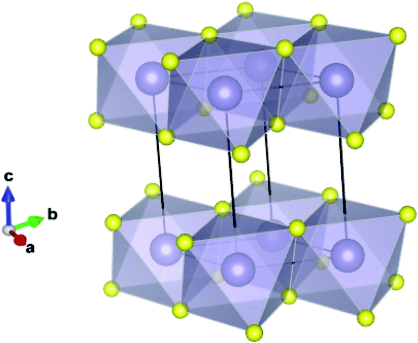 | ||
| Fig. 1 Ground state (2H) structure of SnS2 showing the 2-dimensional bonded plane of edge-sharing octahedra and the conventional unit cell. | ||
SnS2 is also of broader importance as a secondary phase in earth abundant photovoltaic applications, where spontaneous formation has been observed to occur during tin sulfide and copper zinc tin sulfide (CZTS) depositions.17,18 While such formation of tin disulfide ought to be carefully avoided in the photoactive bulk, it remains potentially useful as a n-type buffer layer in such applications, as the wide band gap allows for the transmission of visible light and the low lying conduction band minimum can accept migrating electrons from the photoabsorber.
Over 70 stacking polytypes of SnS2 have been reported to date,19 with thin films grown by spray pyrolysis,20 chemical bath,21 chemical vapour deposition,22 and SILAR methods.14 Numerous nano-forms of SnS2 have also been synthesised, including nano-flowers,23 nano-flakes,10 nano-tubes,24 and quantum dots.25 In addition, a number of other tin sulfide phases (i.e. SnS and Sn2S3) are known to exist,26 with anisotropic properties of their own.27 Unsurprisingly then, reported properties vary with synthesis conditions,28 and thus it is important to identify and analyse the ground state, phase pure SnS2 not just with regards to photocatalytic applications, but all manner of two dimensional devices and metamaterial applications.29
We report the valence band maximum and conduction band minimum energies with respect to the vacuum level and temperature dependent band gaps for phase pure single crystal SnS2, compare these directly with density functional theory and conclude on the applicability of this system for photocatalysis.
2 Methods
2.1 Experimental details
Single crystals were obtained using the chemical vapour transport (CVT) method, which involved the placement of solid iodine and 1![[thin space (1/6-em)]](https://www.rsc.org/images/entities/char_2009.gif) :2 stoichiometric amounts of tin and sulfur in a sealed and evacuated quartz ampoule. A temperature gradient between 850 and 600 °C was enforced across this ampoule for twelve days in order to drive the reaction. Full details of the experimental procedure can be found in Ref. 28, along with additional characterisation such as energy dispersive spectroscopy.
:2 stoichiometric amounts of tin and sulfur in a sealed and evacuated quartz ampoule. A temperature gradient between 850 and 600 °C was enforced across this ampoule for twelve days in order to drive the reaction. Full details of the experimental procedure can be found in Ref. 28, along with additional characterisation such as energy dispersive spectroscopy.
X-ray diffraction (XRD) patterns were taken of the as prepared single crystals to confirm their structures. These were collected on a Bruker D8 instrument with Cu Kα radiation (λ = 1.54 Å) with the samples being held with a Si XRD holder.
Transmission electron microscopy (TEM) results were prepared by dispersing the sample in toluene and drop casting the solution onto a thin carbon support film on a copper grid. The samples were examined at 200 kV in a JEOL 2010 TEM. Selected area electron diffraction (SAED) and convergent beam electron diffraction (CBED) were performed on samples clamped in a folding grid in a Philips EM430 TEM at an accelerating voltage of 200 kV.
Fourier-transform infra-red (FTIR) absorption spectroscopy was performed using a Bruker Vertex 70 V Fourier transform IR spectrometer using a tungsten lamp, a silicon diode detector and a quartz beam splitter. Measurements were performed between 4 and 350 K using a continuous flow helium cryostat. Reflectance and transmittance measurements were performed at an incident angle of 11° relative to the surface normal from which the absorption spectra were calculated.
X-ray photoelectron spectroscopy (XPS) measurements were carried out using a SPECS monochromated Al Kα source (1486.6 eV) at 200 W power with a PSP Vacuum Technology electron analyser. The spectrometer was calibrated using standard Ag 3d5/2 peak at 368.3 eV binding energy with a full-width-half-maximum of 0.6 eV and operated in constant pass energy mode. Low resolution survey spectra were taken at 50 eV pass energy, with regions of interest measured at a higher resolution 10 eV pass energy.
The valence band was also probed by XPS, with the crystals held at a constant sample bias, arbitrarily chosen, of −10.0 V. The conduction band was probed by using inverse photoemission spectroscopy (IPES), using a BaO cathode dispenser electron source and an isochromat NaCl photon detector (PSP Vacuum Technology) to measure the photon energies resulting from the decay of absorbed low energy electrons. Analysis of the measured Fermi edge of a polycrystalline Ag foil indicated instrumental resolutions of 0.3 eV and 0.9 eV for XPS and IPES measurements respectively.
Binding energy scales for the spectra are referenced to the Fermi level determined from the Fermi edge position of polycrystalline Ag foil. Prior to measurement, the single crystals were cleaved by splitting with a steel blade ex situ and vacuum prepared by 500 eV Ar+ ion bombardment for 5 minutes, and annealing at 230 °C for 5 h, to remove surface contaminants.
Finally, Raman spectra were recorded at room temperature with a Raman microscope (Renishaw inVia), using a 532 nm wavelength laser focused through an inverted microscope (Leica), via a 50× objective lens (Leica).
2.2 Theoretical details
The room temperature atomic structure of the SnS2 single crystals, obtained from the XRD analysis, was relaxed using Kohn–Sham density functional theory (DFT),30,31 within the plane-wave project-augmented wave formalism as implemented in the Vienna ab initio simulation package (VASP).32,33 Electron exchange and correlation were described with the generalized gradient approximation (GGA) within the functional of Perdew, Burke and Ernzerhof (PBE).34,35To account for van der Waals interactions, the D3 correction with Becke–Johnson damping was included,36,37 which has been shown to provide superior agreement with experiment over other such relaxation schemes.38 A plane-wave basis set with a 500 eV kinetic energy cut-off, was employed with well-converged k-point sampling of at least 8 × 8 × 6. For the electronic structure and band gap results, hybrid-DFT was employed, incorporating 25% screened Hartree–Fock exchange, i.e. the HSE06 functional.39
3 Results
3.1 Materials characterisation
Single crystal XRD confirmed that the SnS2 crystals had the standard hexagonal crystal structure with P![[3 with combining macron]](https://www.rsc.org/images/entities/char_0033_0304.gif) m1 symmetry (space group 164) corresponding to the ground state 2H polytype with the lattice constants a = 3.649 Å and c = 5.899 Å.28 This is shown as ESI, Fig. S1.†
m1 symmetry (space group 164) corresponding to the ground state 2H polytype with the lattice constants a = 3.649 Å and c = 5.899 Å.28 This is shown as ESI, Fig. S1.†
Fig. 2 (top-left) shows a TEM micrograph of a thin area of a sample which displays twist dislocations. It can be inferred that the crystals are composed of narrow platelets, highlighted by the termination of the dislocations at the platelet edges, as corroborated by the physical appearance of the macroscopic crystals (bottom-centre). Fig. 2 (top-right) also shows the obtained diffraction patterns for a convergent beam electron diffraction in the [0001] direction, from this the lattice parameter a = 3.61 ± 0.04 Å has been determined, which agrees with the average value determined from XRD and simulated TEM for the 2H SnS2 polytype. A CBED pattern in the [0001] direction, shown as the inset of top-right Fig. 2, shows the 6-fold symmetry expected from this direction.
 | (1) |
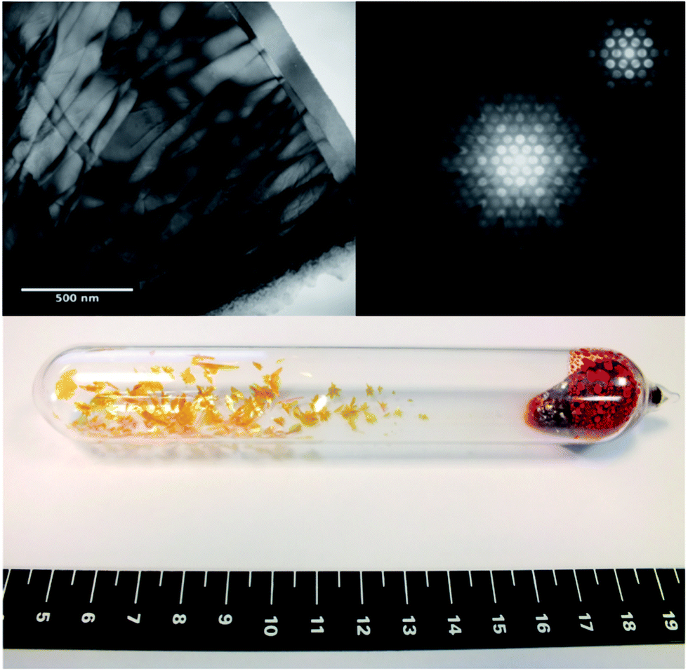 | ||
| Fig. 2 Top left – Bright field transmission electron microscopy of an SnS2 platelet, image near the [0001] zone axis. Top right – Convergent beam electron diffraction pattern near the [0001] zone axis and, inset, detail of the zero order Laue zone from the same sample. Bottom centre – Macroscopic single crystals synthesised from the CVT method, with the scale in centimetres. | ||
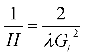
A first order Laue zone (FOLZ) ring was observed which is formed by the intersection of the Ewald sphere with the reciprocal lattice of the crystal in the direction of the incident electron beam, in this case the [0001] direction of the crystal. Using Eqn (1) (where H is the height of the unit cell in real space, G1 is the measured radius of the FOLZ ring and λ is the wavelength of the electrons used), which is derived from the geometry in reciprocal space, the lattice parameter in the [0001] direction can be determined. This was found to be c = 5.3 ± 0.8 Å, which is consistent with the 2H structure. There is however no sign of any higher order Laue zone rings apart from the FOLZ ring, likely owing to the reduced elastic scattering and the increased inelastic background expected at higher scattering angles.
The absence of an inner Laue ring between the zero order reflections (central spot) and the clear higher order Laue zone ring, indicate that phase pure 2H polytype is obtained (see full-size, annotated image in ESI, Fig. S2†). An inner Laue ring would be present because of the larger c lattice parameter for alternate polytypes as the 2H structure has the smallest c lattice parameter possible for this system.40
Fig. 3 shows unpolarized Raman spectra recorded in backscattering geometry. Two peaks are visible, one intense peak at 316.2 cm−1 and a weaker one at 207.9 cm−1. These features are assigned to the two Raman active phonon modes of the 2H polytype of SnS2; that is, with A1g and Eg symmetry, respectively.41,42 The 4H and 18R polytypes are ruled out, as they give three peaks within the 190–225 cm−1 range rather than the single peak observed here.43
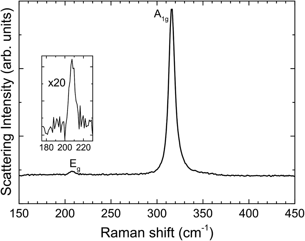 | ||
| Fig. 3 Raman spectrum from SnS2, with A1g and Eg modes indicative of the 2H polytype. The inset shows a 20 times magnification of the Eg mode. | ||
We conclude from the combined X-ray, electron diffraction and Raman results that the single crystals are the ground state 2H polytype of phase-pure SnS2.
3.2 Electronic structure: experiment
XPS core level spectra confirmed both the phase purity of the crystals, and also the successful removal of surface contaminants by sputtering and annealing (see Fig. S3 in ESI†). The combination of valence band XPS and IPES measurements allows the positions of the valence band maximum (EVBM), conduction band minimum (ECBM), and Fermi level (EF) to be determined with respect to the vacuum level (Evac).44 These positions were determined by linear extrapolation of the band edges and secondary electron cut-off, to the baseline, and yielded an ionisation potential (Evac − EVBM) of 6.44 ± 0.07 eV and an electron affinity (Evac − ECBM) of 4.16 ± 0.17 eV. A bandgap (ECBM − EVBM) of 2.28 ± 0.15 eV is thus found that corresponds to the indirect band gap. All of these values are schematically represented in Fig. 4. Given that these techniques have an approximate surface sampling depth of 5 atomic layers it is expected that these values will also be relevant for exfoliated layers and thin films as well as the bulk solid.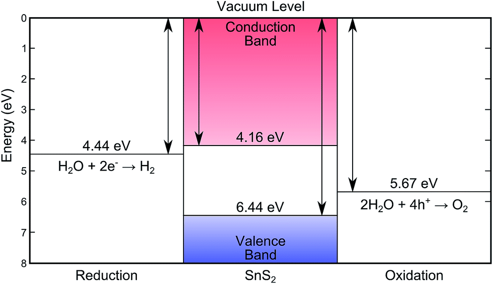 | ||
| Fig. 4 The energy levels of SnS2 as determined by XPS/IPES in this work, showing the desirable band placements for water splitting.7,8 | ||
The macroscopic single crystals of yellow SnS2 were analysed with FTIR spectroscopy between the temperatures 4–350 K, in order to report the temperature dependence of the band gap. The optical absorption spectra are shown in Fig. 5(a) in the form of absorption coefficient squared versus photon energy. The linear portion of these curves is extrapolated to zero to estimate the direct band gap as a function of temperature. These values are then shown as squares in Fig. 5(b). The room temperature (300 K) direct band gap is 2.38 ± 0.01 eV. The indirect band gap was estimated by plotting the square root of the absorption coefficient versus photon energy (see Fig. S4 in ESI†) and extrapolating the linear part of the curves to zero. The values are plotted as circles in Fig. 5(b). It has previously been noted that these methods should be applied with caution to the determination of direct and indirect band gaps that are close in energy.45 However, some support for the methodology is provided here by the relatively close agreement between the 300 K indirect band gap value from absorption of 2.25 eV and the room temperature value determined from XPS and IPES of 2.28 eV.
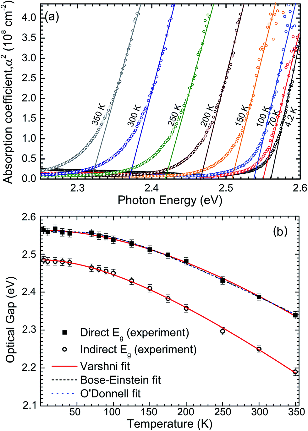 | ||
| Fig. 5 (a) Optical absorption spectra as a function of temperature and (b) corresponding direct (closed squares) and indirect (open circles) band gaps for the same single crystal of tin disulfide. Also shown are Varshni, Bose–Einstein and O'Donnell fits to the direct band gaps and a Varshni fit to the indirect band gaps. | ||
The direct band gap data have been fitted by the standard expressions for the temperature dependence of band gaps, namely the Varshni,46 Bose–Einstein,47 and O'Donnell equations.48 These models account in different ways for the lattice dilation and electron–phonon interactions. All three methods produce a good fit to the data. The coefficients obtained from the fitting procedures are given in Table 1, along with the 0 K band gaps (Eg0) from extrapolation that allow, in principle, for direct comparison with DFT methods. The 0 K direct and indirect band gaps are found to be 2.56 ± 0.01 eV and 2.48 ± 0.01 eV, respectively. The Varshni parameters for the indirect band gap are α = 1.61 × 10⁻³ eV K−1, β = 312.2 K and Eg0 = 2.485 eV. The previously determined direct and indirect band gap values for 2H-SnS2 at 273 and 77 K fall close to the fit lines presented here.45
3.3 Electronic structure: calculation
2-Dimensional semiconductors present both an interesting opportunity and a challenging problem for materials simulation. The failure of DFT to accurately account for long range van der Waals, or London dispersion interactions, is well known,38 as is the difficulty in calculating accurate values for band gaps.49 These two dimensional systems are problematic because their band gap and inter-bonding layer distance are intrinsically linked and accurate modelling of such sensitive parameters has yet to be demonstrated.SnS2 provides a unique opportunity to study these effects in the absence of exotic physical phenomena, such as Dirac cones or topological effects,50 which can arise from partially filled d-orbitals in other systems. With the accurate and well-behaved properties reported for the confirmed ground state structures in the previous section, the opportunity to appraise suitable levels of density functional theory presents itself.
The HSE06 functional has been shown to be superior to other, even higher levels of theory, when it comes to predicting materials band gaps,51 without the need for empirical (+U) parameters. Indeed, for the similar, pseudo-2-dimensional SnS case, this level of theory has been shown to give exceptional agreement with electronic properties of single crystals.27 As such, we assess the performance of HSE06 for electronic-structure calculations on atomic structures obtained directly from experiment and by relaxation with various common DFT functionals. Such consideration allows, uniquely in this study, for the effect of the VdW spacing on electronic structure to be observed alongside direct comparison to single crystal experimental results.
Table 2 compares the lattice parameters and band gaps obtained from HSE06 calculations on the crystal structure obtained at room temperature from single-crystal XRD both without relaxation, and after relaxation with several common DFT functionals. These results show that while the D3 correction is more successful than PBE at reproducing the interlayer spacing in the structure, the subsequent application of HSE06 to this structure yields overestimated band gaps (direct 2.68 eV, indirect 2.14 eV). On the other hand relaxation with the PBE level of theory greatly overestimates the interlayer spacing by more than 15% but does allow for relatively accurate band gaps when compared to experiment (direct 2.62 eV, indirect 2.32 eV).
| DFT procedure | Direct gap (eV) | Indirect gap (eV) | c lattice parameter (Å) | |
|---|---|---|---|---|
| Ionic relaxation | Electronic relaxation | |||
| None | HSE06 | 2.74 (7.03) | 2.29 (−7.66) | 5.899 (0.00) |
| PBE | HSE06 | 2.62 (2.34) | 2.32 (−6.45) | 6.859 (16.3) |
| PBE-D3 | HSE06 | 2.68 (4.69) | 2.14 (−13.7) | 5.808 (−1.54) |
| HSE06 | HSE06 | 2.77 (8.20) | 2.46 (−0.81) | 6.561 (11.2) |
| Experiment | 2.56 | 2.48 | 5.899 | |
The converged atomic coordinates from the HSE06 level gave band gap values of 2.77 eV and 2.46 eV for direct and indirect gap respectively. The fundamental gap is the closest value to experiment reported here but the direct transition is somewhat overestimated. The full electronic structure at this level yielded the band structure diagram for SnS2 as shown in Fig. 6. From this, it is possible to see the highly dispersed conduction band, corroborating the use of this material as an n-type component in electrochemical applications, as band dispersion is inversely proportional to charge effective mass. Similarly the relatively flat valence band between Γ and A shows the low degree of bonding between the distinct layers. The direct band gap of 2.77 eV can be seen, in Fig. 6, to occur at M and the fundamental band gap of 2.25 eV is between the VBM at Γ and the CBM at L. The valence band is found to be composed of a mixture of S 3p and Sn 5s, while the conduction band consists of a mixture of Sn 5s and 5p orbitals, for all HSE06 calculations.
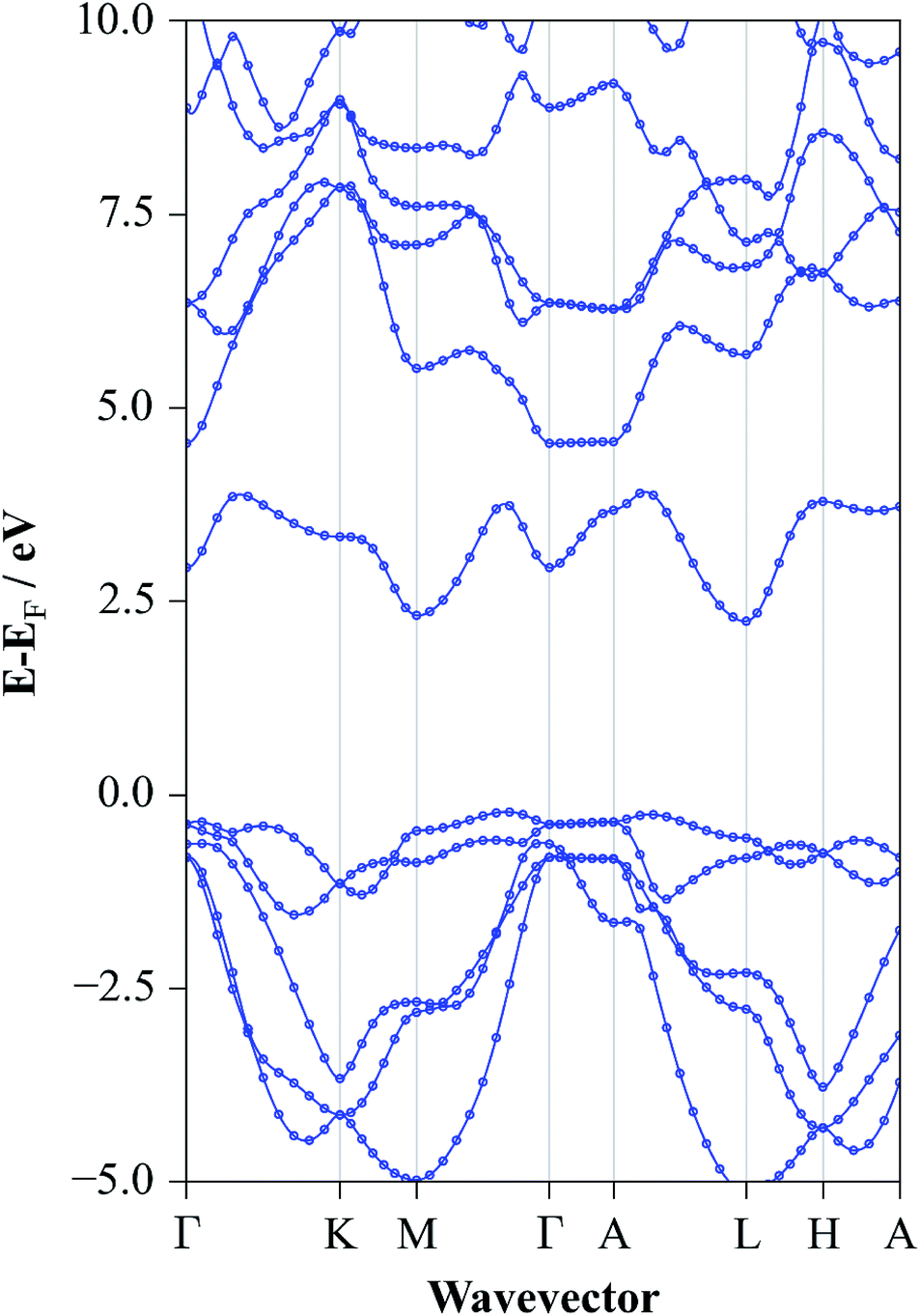 | ||
| Fig. 6 Band structure diagram of SnS2 for the experimentally determined lattice constants at the HSE06/DFT level of electronic structure theory. | ||
All of the methods implemented in this work yield band gap energies that are simultaneously over and under estimated for the direct and indirect gap respectively. This behaviour shows that more than a scissor operator is required to correct the single-particle Kohn–Sham density functional theory description, i.e. a more rigorous description of many body effects may be required for 2D systems. Our results indicate therefore that in order to recover properties for these 2D systems that are as accurate as possible, more sophisticated implementations of DFT are necessary, for example the self consistent screening approach described by Lucero et al.,52,53 and the explicit treatment of electron–phonon coupling. This is due to the sensitivity of the electronic structure on the VdW spacing that is, as of yet, poorly described, even with modern corrections. For now, the most optimal method appears to be allowing structural relaxation with the HSE06 level of theory. While this is the most expensive of the four methods considered here, it offers the lowest deviation from experiment overall with respect to both electronic and structural properties.
4 Discussions & conclusions
The combination of electronic and optical spectroscopy with first-principles calculations can elucidate the origins of the photocatalytic performance of SnS2. The energy levels of the valence and conduction band are almost ideally placed for water photolysis, more so than many other materials receiving intense study in the field currently (see for instance Ref. 54).The band gap of SnS2 is sufficiently wide to straddle both water splitting potentials with suitable overpotentials of 0.77 eV and 0.28 eV for oxidation and reduction respectively. However, due to the n-type nature of SnS2, observed here from the relative position of the work function with respect to the CBM and VBM, alongside favourable band dispersions in the conduction band, this material could also be used in tandem photocatalytic devices. Such devices employ a suitable metal electrode with an n-type photoabsorber to achieve spatially separate oxygen and hydrogen evolution.55 Such a configuration is advantageous as the recombination of oxygen and hydrogen gas to form water is diminished.
It is also expected that these results will have impacts beyond photocatalysis. For example, the energy levels of SnS2 are similar to those found in the n-type material cadmium sulfide (band gap of 2.41 eV and electron affinity of 4.5 eV),56 commonly used in photovoltaic devices. In this way SnS2 could facilitate the elimination of cadmium from these devices, decreasing costs and increasing the deployment of such an important renewable energy source.
We also report the temperature dependent electronic structure relationship for the first time. Extrapolation to a value at 0 K (Eg0 = 2.56 eV, Bose–Einstein fit) provides a reliable reference point for first principles electronic structure calculations. Such realistic benchmarks can greatly facilitate the development of new van der Waals corrections and subsequent improvements of simulation accuracy that we show are currently lacking in the field.
Finally, DFT analysis shows that while many corrections to DFT exist, the optimal method of analysing the electronic structure of such systems is the HSE06 level of theory relaxation of crystal structures. That is to say that in this study, the DFT band gap that is closest in value to the single crystal data, from the several common methods deployed in this work, is the one in which HSE06 was used to fully converge atomic and electronic configurations.
The physical properties reported in this work, combined with the high surface areas readily obtainable with this class of 2-dimensional semiconductors, show that phase pure SnS2 is certainly one of the most promising candidates for water splitting considered to date.
Acknowledgements
LAB was funded by the EPSRC (EP/G03768X/1 and EP/J017361/1) and is now supported through the JSPS (26.04792). TJW and WML were funded by the EPSRC (EP/L505018/1 and EP/G004447/2). AW acknowledges support from the Royal Society University Research Fellowship Scheme. AW and TDV acknowledge membership of the Materials Design Network. P. Jones at the University of Bath is thanked for glass-blowing expertise. Iain Aldous and Laurence Hardwick are acknowledged for access to and assistance with the Raman. The simulated TEM pattern was calculated using the CrystalMaker Software. Images of chemical structure were made using the VESTA software.57References
- R. Priddle, World Energy Outlook, International Energy Agency report, 2012 Search PubMed.
- W. Zhao, Z. Ghorannevis, L. Chu, M. Toh, C. Kloc, P.-H. Tan and G. Eda, ACS Nano, 2013, 7, 791–797 CrossRef CAS PubMed.
- K. F. Mak, C. Lee, J. Hone, J. Shan and T. F. Heinz, Phys. Rev. Lett., 2010, 105, 136805 CrossRef PubMed.
- C. Wang, K. Tang, Q. Aa and Y. Qian, Chem. Phys. Lett., 2002, 357, 371–375 CrossRef CAS.
- J. Wilson and A. Yoffe, Adv. Phys., 1969, 18, 193–335 CrossRef CAS.
- M. G. Walter, E. L. Warren, J. R. McKone, S. W. Boettcher, Q. Mi, E. A. Santori and N. S. Lewis, Chem. Rev., 2010, 110, 6446–6473 CrossRef CAS PubMed.
- M. Ni, J. Jirt, B. Koata, A. Jenkins and A. McNaught, IUPAC Compendium of Chemical Terminology, Iupac technical report, 2009 Search PubMed.
- H. L. Zhuang and R. G. Hennig, Chem. Mater., 2013, 25, 3232–3238 CrossRef CAS.
- S. Chandra, Photoelectrochemical Solar Cells, Gordon and Breach, 1986 Search PubMed.
- Y. C. Zhang, Z. N. Du, S. Y. Li and M. Zhang, Appl. Catal., B, 2010, 95, 153–159 CrossRef CAS.
- Y. Sun, H. Cheng, S. Gao, Z. Sun, Q. Liu, Q. Liu, F. Lei, T. Yao, J. He and S. Wei, Angew. Chem., Int. Ed., 2012, 51, 8727–8731 CrossRef CAS PubMed.
- X. Hu, G. Song, W. Li, Y. Peng, L. Jiang, Y. Xue, Q. Liu, Z. Chen and J. Hu, Mater. Res. Bull., 2013, 48, 2325–2332 CrossRef CAS.
- S. Panda, A. Antonakos, E. Liarokapis, S. Bhattacharya and S. Chaudhuri, Mater. Res. Bull., 2007, 42, 576–583 CrossRef CAS.
- N. Deshpande, A. Sagade, Y. Gudage, C. Lokhande and R. Sharma, J. Alloys Compd., 2007, 436, 421–426 CrossRef CAS.
- Z. Li, W. Luo, M. Zhang, J. Feng and Z. Zou, Energy Environ. Sci., 2013, 6, 347–370 CAS.
- Y. Sun, H. Cheng, S. Gao, Z. Sun, Q. Liu, Q. Liu, F. Lei, T. Yao, J. He, S. Wei and Y. Xie, Angew. Chem., Int. Ed., 2012, 51, 8727–8731 CrossRef CAS PubMed.
- A. Schneikart, H.-J. Schimper, A. Klein and W. Jaegermann, J. Phys. D: Appl. Phys., 2013, 46, 305109 CrossRef.
- M. Z. Ansari and N. Khare, J. Phys. D: Appl. Phys., 2014, 47, 185101 CrossRef.
- T. Jiang and G. A. Ozin, J. Mater. Chem., 1998, 8, 1099–1108 RSC.
- B. Thangaraju and P. Kaliannan, J. Phys. D: Appl. Phys., 2000, 33, 1054 CrossRef CAS.
- R. D. Engleken, H. Mccloud, C. Lee, M. Slayton and H. Ghoreishi, J. Electrochem. Soc., 1987, 134, 2696 CrossRef.
- I. P. Parkin, L. S. Price, T. G. Hibbert and K. C. Molloy, J. Mater. Chem., 2001, 11, 1486–1490 RSC.
- Y. Zou and Y. Wang, Chem. Eng. J., 2013, 229, 183–189 CrossRef CAS.
- A. Yella, E. Mugnaioli, H. A. Therese, M. Panthoofer, U. Kolb and W. Tremel, Chem. Mater., 2009, 21, 2474–2481 CrossRef CAS.
- F. Tan, S. Qu, J. Wu, K. Liu, S. Zhou and Z. Wang, Nanoscale Res. Lett., 2011, 6, 298 CrossRef PubMed.
- L. A. Burton and A. Walsh, J. Phys. Chem. C, 2012, 116, 24262–24267 CAS.
- R. E. Banai, L. A. Burton, S. G. Choi, F. Hofherr, T. Sorgenfrei, A. Walsh, B. To, A. Croll and J. R. S. Brownson, J. Appl. Phys., 2014, 116, 013511 CrossRef.
- L. A. Burton, D. Colombara, R. D. Abellon, F. C. Grozema, L. M. Peter, T. J. Savenije, G. Dennler and A. Walsh, Chem. Mater., 2013, 25, 4908–4916 CrossRef CAS.
- Y. Sun, S. Gao and Y. Xie, Chem. Soc. Rev., 2013, 530–546 Search PubMed.
- P. Hohenberg and W. Kohn, Phys. Rev., 1964, 136, B864–B871 CrossRef.
- W. Kohn and L. J. Sham, Phys. Rev., 1965, 140, A1133–A1138 CrossRef.
- G. Kresse and J. Furthmüller, Phys. Rev. B: Condens. Matter Mater. Phys., 1996, 54, 11169 CrossRef CAS.
- G. Kresse and D. Joubert, Phys. Rev. B: Condens. Matter Mater. Phys., 1999, 59, 1758 CrossRef CAS.
- J. P. Perdew, K. Burke and M. Ernzerhof, Phys. Rev. Lett., 1996, 77, 3865–3868 CrossRef CAS PubMed.
- J. P. Perdew, K. Burke and M. Ernzerhof, Phys. Rev. Lett., 1997, 78, 1396 CrossRef CAS.
- E. R. Johnson and A. D. Becke, J. Chem. Phys., 2006, 124, 174104 CrossRef PubMed.
- S. Grimme, J. Antony, S. Ehrlich and H. Krieg, J. Chem. Phys., 2010, 132, 154104 CrossRef PubMed.
- S. Grimme, S. Ehrlich and L. Goerigk, J. Comput. Chem., 2011, 32, 1456–1465 CrossRef CAS PubMed.
- J. Heyd, G. E. Scuseria and M. Ernzerhof, J. Chem. Phys., 2006, 124, 219906 CrossRef.
- R. S. Mitchell, Y. Fujiki and Y. Ishizawa, Nature, 1974, 247, 537–538 CrossRef CAS.
- A. J. Smith, P. E. Meek and W. Y. Liang, J. Phys. C: Solid State Phys., 1977, 10, 1321 CrossRef CAS.
- V. G. Hadjiev, D. De, H. B. Peng, J. Manongdo and A. M. Guloy, Phys. Rev. B: Condens. Matter Mater. Phys., 2013, 87, 104302 CrossRef.
- S. Nakashima, H. Katahama and A. Mitsuishi, Physica B+C, 1981, 105, 343–346 CrossRef CAS.
- M. Helander, M. Greiner, Z. Wang and Z. Lu, Appl. Surf. Sci., 2010, 256, 2602–2605 CrossRef CAS.
- M. J. Powell, J. Phys. C: Solid State Phys., 1977, 10, 2967 CrossRef CAS.
- Y. Varshni, Physica, 1967, 34, 149–154 CrossRef CAS.
- L. Viña, S. Logothetidis and M. Cardona, Phys. Rev. B: Condens. Matter Mater. Phys., 1984, 30, 1979–1991 CrossRef.
- K. O’Donnell and X. Chen, Appl. Phys. Lett., 1991, 58, 2924–2926 CrossRef.
- J. P. Perdew, Int. J. Quantum Chem., 1985, 28, 497–523 CrossRef.
- H. Zeng, J. Dai, W. Yao, D. Xiao and X. Cui, Nat. Nanotechnol., 2012, 7, 490–493 CrossRef CAS PubMed.
- T. L. Bahers, M. Rerat and P. Sautet, J. Phys. Chem. C, 2014, 118, 5997–6008 CAS.
- M. J. Lucero, I. Aguilera, C. V. Diaconu, P. Palacios, P. Wahnón and G. E. Scuseria, Phys. Rev. B: Condens. Matter Mater. Phys., 2011, 83, 205128 CrossRef.
- J. H. Skone, M. Govoni and G. Galli, Phys. Rev. B: Condens. Matter Mater. Phys., 2014, 89, 195112 CrossRef.
- A. Kudo and Y. Miseki, Chem. Soc. Rev., 2009, 38, 253–278 RSC.
- A. Fujishima and K. Honda, Nature, 1972, 238, 37 CrossRef CAS PubMed.
- J. Lee, W. Lee, T. Park, J. Lee, E. Park, D. Lee, J. Lee and W. Yi, J. Vac. Sci. Technol., B: Nanotechnol. Microelectron.: Mater., Process., Meas., Phenom., 2010, 28, C2B43–C2B46 CAS.
- K. Momma and F. Izumi, J. Appl. Crystallogr., 2011, 44, 1272–1276 CrossRef CAS.
Footnote |
| † Electronic supplementary information (ESI) available. See DOI: 10.1039/c5ta08214e |
| This journal is © The Royal Society of Chemistry 2016 |