
 Open Access Article
 This Open Access Article is licensed under a
 Creative Commons Attribution 3.0 Unported Licence
Soft X-ray spectroscopic studies of the electronic structure of M:BiVO4 (M = Mo, W) single crystals†
V.
Jovic
*ab,
J.
Laverock
cd,
A. J. E.
Rettie
e,
J.-S.
Zhou
f,
C. B.
Mullins
ef,
V. R.
Singh
d,
B.
Lamoureux
d,
D.
Wilson
ab,
T.-Y.
Su
d,
B.
Jovic
g,
H.
Bluhm
h,
T.
Söhnel
ab and
K. E.
Smith
abd
aSchool of Chemical Sciences, The University of Auckland, Auckland, New Zealand. E-mail: vjov001@aucklanduni.ac.nz
bThe MacDiarmid Institute for Advanced Materials and Nanotechnology, New Zealand
cSchool of Physics, H. H. Wills Physics Laboratory, University of Bristol, Tyndall Avenue, Bristol, BS8 1TL, UK
dDepartment of Physics, Boston University, Boston, MA 02215, USA
eMcKetta Department of Chemical Engineering, The University of Texas at Austin, Austin, Texas 78712, USA
fTexas Materials Institute, The University of Texas at Austin, Austin, Texas 78712, USA
gDefence Technology Agency, New Zealand Defence Force, Devonport Naval Base, Auckland 0624, New Zealand
hChemical Science Division, Lawrence Berkeley National Laboratory, Berkeley, CA 94720, USA
First published on 26th October 2015
Abstract
Bismuth vanadate, BiVO4, is a promising material for use as an anode in photoelectrochemical water splitting. However, its conversion efficiency is limited by poor bulk charge transport, which is via small-polarons. We report here the use of a suite of X-ray spectroscopic probes to determine the electronic structure of 0.3–0.6 at% M:BiVO4 (M = Mo or W). The results are interpreted in the context of current theories regarding the influence of doping on the existence of inter-band gap small-polaron states and their effect on the conversion efficiency of BiVO4. Preliminary X-ray absorption and emission measurements reveal that doping widens the band gap from 2.50 to 2.75 eV, whereas the indirect nature of the band gap remains unaffected. X-ray absorption spectroscopy verified that the doping levels did not affect the distorted tetrahedral environment of V5+ in BiVO4. For BiVO4 and W:BiVO4, V L3 resonant inelastic X-ray scattering showed energy loss features related to charge transfer from low lying valence metal/oxygen states to unoccupied V eg conduction band states. A 3.8 eV energy loss feature, coupled with small polaron-like peaks measured in valence band resonant photoelectron spectroscopy of M:BiVO4, point to the population of inter-band gap V 3d states of eg symmetry. The data reveals the existence of a band gap state in the absence of an applied bias in M:BiVO4, linked to small-polaron formation. We tentatively assign it as a deep trap state, which suggests that the improved conversion efficiency of M:BiVO4 relative to the undoped material is largely due to the increased carrier concentration in spite of increased carrier recombination rates.
1. Introduction
Harnessing solar power to generate hydrogen (H2) through photoelectrochemical (PEC) water splitting is a promising approach towards achieving future energy supply security.1,2 There is now a strong incentive to develop metal oxides as alternatives to non-oxide semiconductors (CdTe, CdSe, CdS, Cu(In,Ga)(Se,S)2, GaInP2) for use in PEC water splitting due to their commonly non-toxic nature, stability against photocorrosion and reasonable cost.1,3,4 Bismuth vanadate (BiVO4) is a near ideal candidate in this respect owing to its appropriate band gap (∼2.4 eV), well positioned valence band (VB) potential, stability in the presence of a co-catalyst and promising conversion efficiencies.2,5–11 A bottleneck for the further use of BiVO4 in PEC water splitting is its poor bulk conductivity, the result of electron localization (‘small-polaron’ formation).8,12,13In BiVO4 (a d0 transition metal (TM) oxide), small-polarons form when charge carriers are introduced by doping; small polarons are vulnerable to be trapped.8,14 Instead of flowing freely under an applied bias, the electron is forced to ‘hop’ slowly through the lattice (via V-sites) by thermal assistance, drastically reducing mobility.8,12 BiVO4 possesses the catalytically favourable monoclinic scheelite (ms) structure, composed of edge-sharing BiO8 (Bi3+) dodecahedra in contact with VO4 (V5+) tetrahedra by an apex oxygen atom.6,9,10 Distortions of VO4 and BiO8 units by an electron lone pair (in Bi 6s/O 2p states at the VB maximum), along with poor wavefunction overlap of V–V neighbours in the c-direction, and a large dielectric constant, assist in electron localization.15–17 Based on recent theory, this manifests in electrons occupying empty V 3dz2 states at the CB minimum, with weak delocalization to the adjacent oxygen atoms (filling antibonding V 3d–O 2p states) and a slight elongation of V–O bonds.18 The accompanying adverse electron localization diminishes the availability of charge carriers for surface photoreactions. Intriguingly, it is now well established that doping the BiVO4 lattice with molybdenum (Mo6+) or tungsten (W6+), at V5+ sites in the bulk, can strongly improve the PEC performance.11,19–23 In an effort to shed light on the effects of Mo and W doping on the bulk conductivity and PEC activity, Rettie et al., performed a series of comprehensive electronic transport measurements on 0.3–0.6% Mo/W:BiVO4single crystals. Despite improvements in PEC activity, results verified that the main conduction mechanism in Mo or W doped BiVO4 was still small-polaron hopping (SPH) and that the electron drift mobility remained low: ∼10−4 cm2 V−1 s−1 at 300 K.8,12 Rettie et al., also observed a conductivity anisotropy ratio, σab/σc, in the ab-plane relative to the c-plane of approximately 2.3. The discrepancy was structurally rationalized in terms of a next nearest-neighbour hopping path, only available in the ab plane.12 In agreement with the work of Abdi et al., the results suggest that the improved PEC performance seen in many studies is associated with increased charge carrier concentrations on account of Mo6+ or W6+ (electron donor) substitution at the V5+ site.7,12,21 Results also suggest that the bulk electronic conductivity remains a key obstacle in the PEC activity of BiVO4.21 However, the formation and nature of deep trap states or small-polaron sites, thought to be responsible for the low conductivity, along with their effects on the conversion efficiency, are open to interpretation.
Our current understanding of the structural aspects associated with electron small-polaron formation in M:BiVO4 (M = Mo or W) stems from transport data and theoretical calculations. This forms a foundation for interpreting the material's electronic structure and electron localization from an X-ray spectroscopic perspective, as recently pointed out by Kweon et al.18 In this paper, we focused on detailed measurements of the electronic structure of BiVO4, 0.6 at% Mo:BiVO4 and 0.3 at% W:BiVO4 single crystals using X-ray absorption spectroscopy (XAS), X-ray emission spectroscopy (XES), resonant inelastic X-ray scattering (RIXS) and X-ray photoelectron spectroscopy (XPS). Preliminary measurements were aimed at (i) probing the fundamental electronic structure of pure and doped BiVO4 in an effort to standardise our results and to build on earlier spectroscopic studies, and (ii) at evaluating the influence of Mo or W on the electronic band gap. Next, we focused on the identification of localized electron (small-polaron) sites, which have recently been theoretically predicted to result in the presence of inter-band gap spectroscopic fingerprints.18 The data is interpreted in the context of current theories aimed at linking the influence of Mo/W doping on the PEC performance of BiVO4.
2. Experimental
2.1 Materials
High quality single crystals of BiVO4, 0.6 at% Mo doped BiVO4 and 0.3 at% W doped BiVO4 were grown by a floating zone method in an optical image furnace at the University of Texas at Austin.8 Details regarding the crystal growth and characterization along with the results of PEC performance and transport measurements have been comprehensively reported in our earlier publications.8,122.2 Spectroscopic methods
Single crystal boules were cleaved ex situ to give rectangular plates which revealed mirror-like faces. Soft X-ray spectroscopy (XAS, above-threshold XES and RIXS) data was collected at beamline 8.0.1 of the Advanced Light Source (ALS), Lawrence Berkeley National Laboratory (LBNL). XAS data were collected in the surface sensitive (∼10 nm) total electron yield (TEY) mode by measuring the sample drain current, and in the bulk sensitive (∼100 nm) total fluorescence yield (TFY) mode. The energy scales of XAS spectra at the V L- and O K-edges were calibrated with reference to the Ti L- and O K-edge XAS spectra of rutile TiO2. Spectral resolution was ∼200 meV at full width at half maximum (FWHM). Agreement between TEY and TFY spectra indicated that BiVO4 did not charge during measurements, and that the TEY signal was also illustrative of the bulk. O K-edge XES and V L3 edge RIXS data were calibrated with reference to the Lα1,2 and Lβ1 second order emission lines of a Zn metal, and using the elastic scattering peaks of V Lα emission spectra. The XES spectral resolution was 700 meV. For RIXS measurements at the V L3-edge, the photon resolution was ∼300 meV. Both XES and RIXS spectra were recorded in a 90° scattering geometry, i.e. the angle between the wavevectors of the incident and scattered X-rays. Thus, the incident X-rays were at 45° relative to the surface normal of the sample. This decreases contributions from the elastic feature in the spectra by reducing elastic scattering from the material for linearly polarized light in the scattering plane, as the Brewster angle is 45°.24 The analysis chamber pressure was below 5 × 10⁻⁹ Torr during measurements. XPS data were collected at beamline 11.0.2 of the ALS. The UHV chamber base pressure was below 5 × 10⁻⁹ Torr for measurements. VB spectra were collected with 275 eV photons and calibrated against the 4f peaks of a metallic gold foil in electrical contact with the sample.2.3 Data analysis
To remove undesirable high frequency noise components from the intensity signals of noisy spectra, a Finite Impulse Response (FIR) Low Pass (LP) filtering method was implemented.25,26 The FIR LP filter was designed by first modelling the intensity signal in the time domain where its duration was set to 1 second. The signal was then transformed to the frequency domain using the Fourier Transform and its spectral components were observed. This is shown in ESI Fig. 1(a)† for an example BiVO4 V L3 RIXS spectrum (hν = 515.2 eV).27 The FIR LP filter used was designed with start and stop cut-off frequencies of 80 and 100 Hz, respectively.25 The filter eliminates all frequency components above 100 Hz, while not modifying, that is, passing, all frequency components between 0 and 80 Hz. The 80–100 Hz frequency range is known as a transition band of a practical filter in which frequencies are progressively attenuated. An inherent feature of a practical FIR filter is that it reduces the number of signal samples during the filtering process. The number of samples reduced by the filtering process increases as the transition band of an FIR filter is shortened. The non-filtered and filtered intensity signals are shown in the time domain in ESI Fig. 1(b).† High frequency noise components were successfully removed, leaving a smooth signal which accentuates desired low frequency characteristics. The designed filter was found to produce the most optimal results out of a number of other FIR LP filters with different cut-off frequencies. Filters based on wavelets offering other advantages over the FIR LP method are described in the ESI.†263. Results and discussion
Fig. 1(a) shows V L3,2-edge XAS, TEY (black) and TFY (red), for (a.) BiVO4, (b.) 0.6% Mo:BiVO4 and (c.) 0.3% W:BiVO4. Spectra are dominated by two regions; L3 (excitation from 2p3/2 core levels to unoccupied CB V 3d states) and L2 (excitation from 2p1/2 core levels to unoccupied CB V 3d states). The regions are separated by 6.65 eV due to the spin–orbit coupling of the 2p core-hole, in agreement with the work of Cooper et al.16 The L3 edge further splits into two main regions; the eg (516.3 eV) and t2g (518.5 eV) states, separated by 2.14 eV (which is related to the ligand field splitting parameter, 10Dq).28 Peaks ‘I’ and ‘III’, at 515.4 and 517.2 eV, respectively, are triplet states arising from atomic multiplet effects associated with the core-hole following transitions from occupied 2p3/2 states to unoccupied 3d states (eg and t2g) of V5+ (i.e. p–d orbital interactions).28 These features, having wavefunctions with strong ligand character, are mixed through spin–orbit interactions and Coulomb repulsion into the L3 edge. They provide information regarding charge transfer between oxygen ligands and d0 metal sites using V L3 RIXS (as will be discussed).28 The L2 edge has a similar shape to the L3 edge; however, as the lifetime broadening at the L2 edge is shorter, the spectral features are not obvious. Collectively, the spectra provide evidence of a distorted tetrahedral environment of V5+ in the monoclinic scheelite structure of BiVO4. The d-states of the dopant distribute near the bottom of the VB (bonding M–O features) and CB (anti-bonding M–O features).29 However, spectral changes with doping are not evident owing to their low concentration in the lattice and similar atomic radii to V (giving only a slight elongation of the M–O bond).29 Furthermore, formation of a small-polaron at V 3dz2 states is accompanied by partial electron delocalization to the surrounding oxygen atoms, resulting in a localised distortion due to V–O bond elongation.18 This is expected to produce a weak spectral feature at energies within the electronic band gap.18 However, the samples already have a strongly distorted local environment (due to the core-hole). Thus, the small-polaron (a state bound to a weak local distortion), and its spectroscopic fingerprint, will be strongly susceptible to core-hole effects. This makes it difficult to detect simply through XAS or non-resonant XES (Fig. 2(a)). Spectroscopic evidence of small-polaron-like features is shown in later text. | ||
| Fig. 1 (a) V L3,2 XAS in the TEY (black) and TFY (red) modes for (a.) BiVO4, (b.) 0.6% Mo:BiVO4 and (c.) 0.3% W:BiVO4. (b) O K-edge XAS in the TEY (black) and TFY (red) modes for (a.) BiVO4, (b.) 0.6% Mo:BiVO4 and (c.) 0.3% W:BiVO4. Spectra are vertically offset for clarity. | ||
 | ||
| Fig. 2 (a) O K XES spectra for (1.) BiVO4, (2.) 0.6% Mo:BiVO4 and (3.) 0.3% W:BiVO4 collected with an incident photon energy of 560 eV. (b) BiVO4 O K-edge RXES. (c) 0.6% Mo:BiVO4 O K-edge RXES. (d) 0.3% W:BiVO4 O K-edge RXES. | ||
Fig. 1(b) shows O K-edge XAS in TEY (black) and TFY (red) modes for (a.) BiVO4, (b.) 0.6% Mo:BiVO4 and (c.) 0.3% W:BiVO4. O K-edge XAS involves transitions from occupied 1s core levels to empty O 2p states, thus providing an insight into unoccupied metal states due to hybridization with oxygen valence states.30 Characteristic peaks at 530.8 eV (labelled I) and 532.1 eV (II) are indicative of O 2p–V 3d hybridization and in agreement with the tetrahedral crystal field split V eg and t2g states.31 The t2g feature is a contribution of two peaks (at 531.7 eV and 532.5 eV) owing to the V 3d orbital non-degeneracy.16 A strong feature at 535.7 eV (III) (particularly obvious in the TFY spectra of each material) is related to Bi 6p states in the bulk.16 A feature at 537.3 eV can be clearly resolved in the TFY spectra and is prominent in undoped BiVO4 and in Mo:BiVO4 but absent in W:BiVO4. Its origin will be addressed below, in the context of O K-edge resonant XES. Finally, a broad band extending beyond 538 eV indicates mixing of metal 4sp and O 2p electrons.31 As noted, oxygen states will hybridize with dopant d-states, however, due to low doping levels and strong core-hole effects, spectra do not reflect the presence of Mo and W in the systems.
O K-edge XES (transitions from O 2p states to O 1s core level) was used to probe the materials occupied partial density of states (pDOS). Fig. 2(a) shows XES for (1.) BiVO4, (2.) 0.6% Mo:BiVO4 and (3.) 0.3% W:BiVO4 collected at an incident photon energy of 560 eV (well above the absorption threshold). A broad feature from 520–530 eV is indicative of a VB dominated by O 2p states, typical of TM oxides. The peak at 526.5 eV (I) signifies emission from O 2pπ states near the VB maximum and experiences a ∼0.2 eV low energy shift after 0.6% Mo doping. A similar observation is seen with 0.3% W doping and suggests weak broadening of the bulk band gap energy with doping, verified below. Emission from hybridized O sp2/V 3d states near the VB centre is indicated by a feature at 524.7 eV (II).16 Spectral broadening near the bottom of the VB is due to emission from hybridized O sp2–Bi 6p states at 523 eV (III).16 A low energy feature at 510.5 eV (IV) is associated with the V Lα1,2 emission line (transitions from V 3d to V 2p states). Similarly, a small peak at 518 eV (10 eV below the VB maximum) is likely related to V Lβ emission. This is based on the similar energetic separation (∼6.65 eV) as the spin–orbit splitting of the V L3 and L2 absorption features in Fig. 1(a). Previously, this feature was also proposed to be associated with Bi 6s states due to the suppression of the V Lβ emission by the more intense O Kα emission line (O 2p → O 1s).15,32 Due to the 3+ charge of Bi in BiO8, the 6s states have an electron lone pair which interacts with O 2p states. This results in an occupied antibonding state with minority 6s character at the VB maximum and majority 6s character at the minimum.13,15 Bi 6s–O 2p coupling, and the resulting lone pair of electrons, distorts the VO4 and BiO8 units. This weakens the antibonding destabilization.15 The distortion may also result in the poor wavefunction overlap of V sites in the c-direction, possibly aiding in electron localization (this is further addressed in the text below).16
By tuning the photon energy to that of an XAS feature, resonant XES (RXES) can be used to provide site specific DOS for the associated chemical environment. Fig. 2 also shows O K-edge RXES data for (b) BiVO4, (c) Mo:BiVO4 and (d) W:BiVO4 excited at select energies along the O K-edge absorption edge. All spectra show emission at; (i) 526.5 eV (from O 2pπ states); (ii) 524.7 eV (from O sp2/V 3d states); (iii) 523 eV from O sp2/Bi 6p hybridized states, (iv) 510 eV due to emission from V Lα states and; (v) weak Bi 6s/O 2p states at 518 eV. Resonance with the eg peak (530.7 eV) results in quasi-elastic scattering (at the same energy) which is quenched by fluorescence signals at higher resonance energies. At resonance energies near the onset of the O K-edge absorption (i.e. where electrons are promoted to unoccupied valence states near the CB minimum) emission from O sp2/V 3d states is enhanced. At higher energies, emission features from O 2p states predominate. Resonance at 537.3 eV (with a feature in the bulk sensitive TFY plots of BiVO4 and 0.6% Mo:BiVO4) gives a distinct enhancement of the V Lα emission feature at 510 eV. This is coupled with an enhancement V Lα feature at 518 eV and overall a broadening of the VB. Thus, we associate this feature with emission from hybridized V–O sp2 states.
We next consider the effects of doping on the size of the BiVO4 bulk band gap. Fig. 3 compares O K-edge XAS TFY (red) with non-resonant O K-edge XES (black) for BiVO4, 0.6% Mo:BiVO4 and 0.3% W:BiVO4. Corresponding first derivative plots are shown in the right panels of Fig. 3. XES data were collected at hν = 550 eV, which is sufficiently high above the absorption threshold to extract data regarding the high energy VB onset. At higher energies, closer to the ionisation potential, other processes contribute (i.e. double excitations, ionisation, etc.) and overestimate the energetic onset. With respect to XAS, the O K-edge is ‘less complex’ than the V L-edge due to core-hole screening from band edge electronic states of the metal. Screening also lowers core-hole effects (perturbations to the system which shift spectra to lower energies), resulting in a more direct picture of the energetic onset at the conduction band. At the O K-edge, the core-hole shift is equal for all crystals studied here (∼1 eV).33 Thus, any evolutions with doping are robust irrespective of the shift. On this basis, the bulk band gap energy can be determined from the separation between the first derivative minima and maxima of the XES and XAS spectra, respectively. In undoped BiVO4, the band gap is determined to be 2.50 ± 0.1 eV (corresponding to transitions from occupied O 2p states at the VB maximum to unoccupied V 3d states at the CB minimum).17 This is in agreement with recent values found by X-ray spectroscopy.34 A band gap of 2.75 ± 0.1 eV was found for 0.6% Mo:BiVO4. The 0.25 eV broadening with Mo doping is consistent with a generalized gradient approximation (GGA) predicting an increase in the band gap energy from 2.08 eV to 2.14 eV after 1.04% Mo doping.29 We note that this method underestimates the band gap energy relative to experimental measurements.29 The band gap energy is roughly the same with 0.3% W doping. These experimental values are slightly larger than the 2.40 eV energies found for the crystals using diffuse reflectance UV-vis spectroscopy and incident photon conversion efficiency (IPCE) spectra.8 The broadening of the gap is also consistent with an increase in the PEC activity of doped BiVO4, due to improved transport properties.22 However, this increase in PEC activity is also likely related to changes in the ratio of the effective mass between an electron–hole pair with doping. In pure BiVO4, the effective mass of charge carriers is thought to be light and equal, which can lead to rapid recombination rates.15,29 Doping has been predicted to induce significant variation in the effective masses between electron–hole pairs, particularly along different directions in reciprocal space, which facilitates charge separation and aids in PEC performance.29
 | ||
| Fig. 3 Left panels; O K-edge XES (black) and O K-edge XAS TFY (red) for BiVO4, 0.6% Mo:BiVO4 and 0.3% W:BiVO4. The XES spectra were taken at hν = 550 eV. Right panels; first derivative plots for the plots at left. | ||
Resonant inelastic X-ray scattering, RIXS, can also be used to probe the electronic transitions (direct or indirect) between high and low energy points of the VB and CB, respectively. The direct or indirect nature of the band gap has a strong effect on H2 production and has been an aspect of debate in BiVO4.13,29,34,35 Briefly, the VB maximum and the CB minimum are distinguished by particular wavevectors in k-space.36 In an indirect band gap (Fig. 4(a)), e−–h+ angular momenta differ, thus radiative recombination rates are low due to the violation of conservation of momentum.35 Non-radiative recombination occurs at grain boundaries or point defects.37 In a direct band gap, angular momenta are equal and recombination is more dynamic (shown by time resolved microwave conductivity on anatase and rutile TiO2).38,39 In this process, electron excitation to the CB manifests in an intermediate state with a core-hole. Decay of a valence electron to the core-hole conserves momentum between the initial and final states, thus emission occurs from valence states at the same point along the E-k dispersion as for absorption.34,40 The use of RIXS as a probe of vertical transitions in E-k space was elegantly shown by Cooper et al., on BiVO4 thin films spin coated on silica substrates.34
 | ||
| Fig. 4 (a) The indirect (left) and direct (right) electronic band gaps. (b–d) Plots of O K-edge XES spectra collected at three energies near the onset of the O K-edge XAS. The high energy shift of VB onset with increasing photon energy verifies that the band gap of the material is indirect and unaffected by Mo or W doping. | ||
Fig. 4 also shows O K-edge RIXS for (b) BiVO4, (c) 0.6% Mo:BiVO4 and (d) 0.3% W:BiVO4 collected at 530.8 eV, 532.6 eV, 534.4 eV (in the vicinity of the O K-edge absorption threshold). The crystals show a shift in the VB maximum with increasing excitation energy (i.e. as electrons are promoted to higher energies beyond the onset of the CB). Spectra signified by black lines were collected with incident photon energies of ∼530.8 eV (just above the onset of absorption). Here, a core electron moves near the CB minimum. The coherent part of the emission comes from valence states at the same momentum (vertical transition in the dispersion relation). With increasing energy, we move away from the CB minimum and see that the spectra shift to higher energies. Thus, emission occurs from states closer to the VB maximum, which happens to be at a different k-point relative to the CB minimum. The data suggests that BiVO4 has an indirect gap (lower in energy than the direct gap) which is unaffected by doping. The observation of an indirect gap in BiVO4 is consistent with recent experiments and with theory predicting separations of 2.08–2.17 eV between the VB maxima and CB (found at different k-points along the L and M line).17,29,34,41 As stated earlier, the GGA method predicting a marginal increase in the band gap energy with doping, also predicted no effect on the indirect gap with doping.29 The use of RIXS as a probe of the band gap nature should also be approached with some caution. For instance, Walsh et al. found that BiVO4 has a direct band gap between the A points of the Brillouin zone corresponding to an energy of 2.21 eV.13 They showed that the A point of the valence band has a strong Bi 6s component, and only very weak V 3d character. The O K-edge RIXS (Fig. 4) shows an indirect gap. Here, the excited states (CB) are predominantly V 3d states. Thus, it may be that fluorescence from the Bi 6s at the very top of the band, near the A point, is suppressed in our measurements, in favour of fluorescence from the deeper states that mix with vanadium. In that case, it would look indirect to the RIXS measurements performed here, but would formally be a direct band gap.
As RIXS probes excitations related to valence states near the Fermi level, it also provides insight into low energy crystal field excitations and charge transfer events between ligand–metal and metal–metal sites.42 In particular, RIXS is a sensitive probe of local perturbations in the system on account of Mo6+ or W6+ doping at V5+ sites. Fig. 5(a) displays the V L3-edge RIXS spectra for BiVO4, collected at incident photon energies of (a.) 516.4 eV (on the V L3 eg peak), (b.) 516.2 eV, (c.) 515.9 eV, (d.) 515.3 eV and (e.) 515.2 eV. These energies correspond to excitation along the V L3 eg onset (as shown at the inset of plot (a)). Fig. 5(b) shows the spectra on an energy loss scale (i.e. referenced to the incident photon energy). BiVO4 is a d0 compound, therefore, the strong signal to noise ratio in the RIXS spectra was anticipated.43 Accordingly, we used the Finite Impulse Response (FIR) Low Pass (LP) filtering method, described in the data analysis section, in an attempt to filter the intensity signal by removing noise components.25–27 The raw non-filtered signals are shown in red and the FIR LP filtered signals are shown in black.
 | ||
| Fig. 5 (a) V L3-edge RIXS spectra for BiVO4. The spectra have been vertically offset for clarity. The excitation energy for each spectrum is indicated on the plot. (b) The V L3-edge RIXS spectra for BiVO4 on an energy loss (charge transfer) scale. In all plots, the raw, non-filtered, signals are shown in red and the FIR LP filtered signals are shown in black. | ||
In V L3-edge RIXS (as with other transition metals), three typically different processes are likely to occur, (i) fluorescence from occupied VB states, (ii) charge transfer excitations between hybridized metal–oxygen states and metal–metal sites, (iii) crystal field excitations (transitions within the metal d-manifold).24 Resonance on the eg peak (516.4 eV) results in a spectrum dominated by fluorescence at ∼511 eV (emission from hybridized O sp2/V 3d states) and by elastic scattering of incident radiation. As the incident photon energy is tuned further toward the onset of absorption, the RIXS cross section becomes more Raman-like and less fluorescence-like. This accounts for the apparent shift in the fluorescence feature from 511 eV, in spectrum ‘a’, to lower energies, in spectra d–f, and also explains the change in shape of the main emission feature. Likewise, resonance near the multiplet state (spectra d–f) enhances signals related to charge transfer processes. Accordingly, the peak broadening between 510–508 eV (−6 eV through −8 eV on the energy loss scale) results from charge transfer excitations from O 2p–V 3d sites: O 2p6 V 3dn → O 2p5 V 3dn+1 (a direct RIXS transition).43 Based on spectral broadening, and on recent theory, the charge transfer most likely corresponds to transitions from low lying V–O states to low lying empty V eg states.18 Below 4 eV from the elastic peak, spectra are dominated by scattering features; dd excitations in the metal d-manifold. In particular, an inelastic scattering at ∼1.0 eV (I) (energy loss) results from transitions within the crystal field (i.e. inter-orbital V 3d eg → eg transitions), in agreement with recent studies.16 We also address, in the following text, the development of a weak shoulder feature at 3.6–3.7 eV on the energy loss scale.
Fig. 6(a) shows V L3-edge RIXS spectra for 0.3% W:BiVO4, excited at (a.) 516.4 eV, (b.) 515.9 eV, (c.) 515.2 eV and (d.) 514.9 eV (shown at the inset). Fig. 6(b) shows the spectra on an energy loss scale. As for BiVO4, resonating on the eg peak results in the characteristic fluorescence signal at 511 eV related to emission from O sp2/V 3d. Resonance at lower energies results in strong broadening of the main fluorescence feature below 510 eV (−6 eV to −8 eV energy loss) due to O 2p6 V 3dn → V 3dn+1 O 2p5 charge transfer processes. Broadening is slightly more prominent in comparison to that in pure BiVO4. As mentioned earlier, the spectra of BiVO4 and W:BiVO4 both show a small shoulder peak at ∼3.8 eV energy loss when resonating at lower energies. In both materials, the lower CB is predominantly V 3d/O 2p in character. Crystal field splitting and compression in the z-direction leaves the V 3dz2 states near the CB minimum.18 As stated in earlier text, DFT/Hartree–Fock theory (which accounts for exchange–correlation potentials and many-body electron interactions) predicts that excess electrons occupy the V 3dz2 states, delocalizing to V 3d–O 2p states of the surrounding oxygen ligands and elongating V–O bonds.18 Polaron formation was expected to result in a very weak spectral feature near the conduction band minimum. Based on the theory, transitions from low lying V–O valence states to the polaron band should result in an energy loss feature at ∼4.8 eV. On this basis, we speculate that the development of feature at ∼3.8 eV energy loss is possibly related to charge transfer from the lowest lying V–O states to polaron states within the band gap. However, precise energies may vary based on theoretical and empirical accuracy. This, and the V 3dz2 nature of the states, is examined in further detail below.
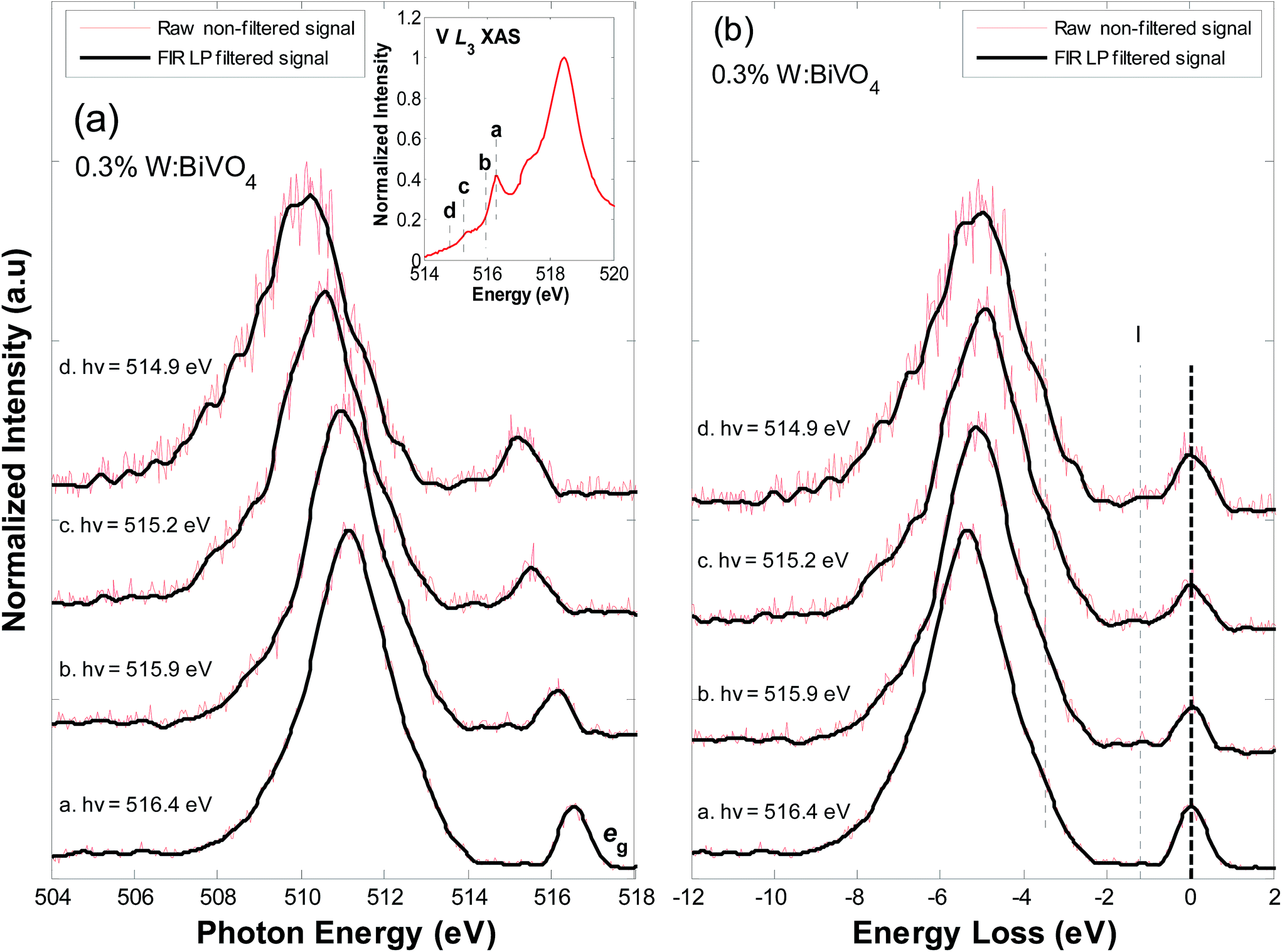 | ||
| Fig. 6 (a) V L3-edge RIXS spectra for 0.3% W:BiVO4. The spectra have been vertically offset for clarity. The excitation energy for each spectrum is indicated on the plot. (b) The V L3-edge RIXS spectra for 0.3% W:BiVO4 on an energy loss (charge transfer) scale. The raw, non-filtered, signals are shown in red and the FIR LP filtered signals are shown in black. | ||
Apart from V L3 RIXS, empirical signatures of polaron states are likely to be seen by XPS as local perturbations from the core-hole are minimized. Fig. 7(a) shows valence band XPS data for BiVO4, 0.6% Mo:BiVO4 and 0.3% W:BiVO4. The spectra show characteristic contributions from Bi 6s states (10 eV), Bi 6p and V 3d states (8 and 6 eV, respectively) and O 2p states (6 eV below the VB maximum to its onset).15 A peak appears above the maximum in the doped samples (∼1.8 eV in binding energy, marked by *). A similar feature was seen by Feng et al., in CeO2 upon reduction of Ce4+ to Ce3+ and was assigned to localized electrons (‘small polarons’) occupying a narrow Ce 4f electronic state in the band gap.44 To further probe the origin of this feature, we show resonant VB XPS data for 0.3% W:BiVO4 at excitation energies of 510 eV, 516 eV and 518.5 eV (Fig. 7(b)). These energies correspond to resonance with the V L3 XAS feature at 516 eV (i.e. resonance with the eg states), the L3 feature at 518.5 eV (resonance with the t2g states) and off resonance at 510 eV, as shown in the inset of Fig. 7(b). A distinct increase in the intensity of the feature occurs following resonance at 516 eV (i.e. on the eg peak). The intensity decreases with resonance at 518.5 eV (on the t2g peak). The observations correlate with theory suggesting that the addition of an electron to BiVO4 creates localized states within the band gap which are V 3dz2 in nature.18 Accordingly, the peak seen here may signify population of low lying V 3d states. As this feature occupies the lower half of the band gap, it may also signify the presence of deeply trapped states formed when BiVO4 is W doped, as described by Abdi et al.21 Such an observation would also be consistent with the rapid electron–hole pair recombination rates observed in W:BiVO4.21 Despite having a negative effect on recombination rates, Abdi et al. found that the increased carrier density induced by W doping improves the overall photoresponse.21 This verified that the bulk electronic conductivity is one of the primary setbacks in the PEC performance of BiVO4. For instance, in our earlier study, we could not detect a measurable photocurrent from undoped BiVO4 electrodes due to the materials inherently low bulk conductivity. Thus, PEC testing was done with the Mo and W doped samples which showed photocurrents of ∼0.4 mA cm−2 at 1.2 V versus RHE (using the (001) faces).8 Qualitatively, this observation of improved PEC water splitting performance from the n-type single crystals is in agreement with earlier studies performed using n-type polycrystalline films of Mo/W:BiVO4.2 IPCE spectra were consistent with those of polycrystalline anodes which showed tails extending to 520 nm. However, direct comparisons with polycrystalline anodes is difficult due to the different Mo or W loading percentages and the fact that PEC tests were completed on the exposed (001) faces, whereas polycrystalline anodes have various crystallographic orientations. In this respect, interpretation of PEC activity in single crystal is also not complicated by effects such as grain boundaries. Therefore, single crystals can be considered near model systems for relating transport properties to PEC activity, as reported earlier.8,12 It is also interesting that the 1.8 eV VB feature (Fig. 7(a)) does not scale with the doping percentages, but is most prominent in the 0.3% W doped crystal. This is consistent with our transport measurements, where the Mo and W doped crystals showed the same conductivity despite different doping concentrations.8 The result could indicate that W is a more effective dopant, at least in terms of increasing the carrier concentration. It is also surprising that the spectral weight of the feature in Fig. 7(a) is of relatively high intensity, particularly as the maximum doping is 1 at% (i.e., expected 1% V4+). In contrast to RIXS, XPS is highly surface sensitive. Thus, VB spectra may also reflect the presence of native V4+ surface sites due to self-doping from oxygen off-stoichiometry initiated by crystal growth. The oxidation state of the doped single crystals was checked by V 2p core level XPS (ESI Fig. 4†). V 2p3/2 and 2p1/2 spin orbit split (SOS) peaks at 516.9 and 524.0 eV (SOS = 7.1 eV) in a 2![[thin space (1/6-em)]](https://www.rsc.org/images/entities/char_2009.gif) :1 peak ratio, typical for the V5+ oxidation state. Weak shoulder peaks at 515.5 eV signified the expected, but weak, presence of V4+. Thus, self-doping effects are minimal or absent and the VB signal indicating V4+ is likely associated with small-polaron and electron trap states within the band gap.
:1 peak ratio, typical for the V5+ oxidation state. Weak shoulder peaks at 515.5 eV signified the expected, but weak, presence of V4+. Thus, self-doping effects are minimal or absent and the VB signal indicating V4+ is likely associated with small-polaron and electron trap states within the band gap.
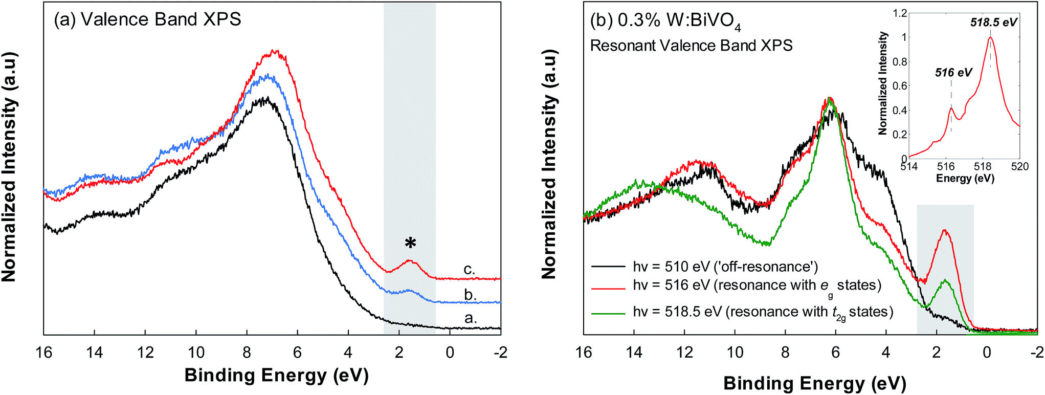 | ||
| Fig. 7 (a) Valence band XPS spectra for (a.) BiVO4, (b.) 0.6% Mo:BiVO4 and (c.) 0.3% W:BiVO4 collected using an incident photon energy of 275 eV. (b) 0.3% W:BiVO4 resonant valence band spectra collected at incident photon energies of 510 eV, 516 eV and 518 eV. | ||
We can again consider the effects of doping on the increased PEC activity of BiVO4.7 Our previous study verified that electron mobility in M:BiVO4 is low, but consistent with small-polaron conduction, ∼10−4 cm2 V−1 s−1, between 250–400 K.8 Furthermore, a conductivity anisotropy ratio of ∼2.3 was found between the ab-plane and c-plane.12 Poor electron mobility was attributed to structural disorder. Specifically, the anisotropy was rationalized in terms of additional ‘Next-Nearest-Neighbour’ (NNN) transfers in the ab plane relative to only nearest neighbour hopping along the c-axis.8,12 The electronic motion was also associated with narrow electronic energy bands near the bottom of the conduction band. In this respect, direct spectroscopic observation of small-polaron-related states in M:BiVO4 may also lend support to recent theory and transport measurements regarding the effects of doping on the conductivity.18 Specifically, increased charge carrier concentrations induced by doping may result in a higher probability of polaron wavefunction overlap with positive effects on carrier transport. This assists in the migration of photo-generated charge within the BiVO4 bulk, making more charge carriers available for transport to the underlying conducting glass from where they are channelled to the cathode for H2 production. However, doping levels for such effects may have to be considerably higher than seen here.18
4. Conclusion
This study used XAS, XES, RIXS and XPS to probe the electronic structure of M:BiVO4 (M = Mo or W), a promising material for use as an anode in PEC water splitting. The data was interpreted in the context of current theories regarding the influence of Mo/W doping on the existence of inter-band gap small-polaron states and their possible effects on the PEC performance of BiVO4. Initially we confirmed that 0.3–0.6 at% Mo and W doping did not affect the indirect nature of the electronic band gap and the catalytically active monoclinic scheelite structure of BiVO4. Ensuing M:BiVO4 V L3 RIXS showed excitations from hybridized metal/oxygen states to empty V 3d states, and crystal field excitations within the V 3d-manifold. Furthermore, V L3 RIXS of pure and W:BiVO4 also showed the first likely sign related to the population of inter-band gap small-polaron states. A small-polaron-like peak was evident in the valence band XPS spectra of M:BiVO4 and intensified when the incident photon energy was resonant with the V L3 eg absorption edge. This further pointed to the presence of electrons localized in V 3dz2 states of M:BiVO4, in agreement with recent theory. The possible association of this feature with a deep trap state suggests that the improved PEC efficiency of M:BiVO4 relative to undoped BiVO4 is largely due to an increase in charge carrier concentration despite higher charge carrier recombination rates. We hope that this study on the electronic structure of M:BiVO4 will guide further spectroscopic studies related to the nature of detrimental electron localization, therefore pointing to ways of maximizing the materials STH efficiency.Acknowledgements
The Boston University program is supported by the Department of Energy under Grant No. DE-FG02-98ER45680. The Advanced Light Source is supported by the U.S. Department of Energy under Contract No. DE-AC02-05CH11231. AJER and CBM gratefully acknowledge the U.S. Department of Energy (DOE) Grant DE-FG02-09ER16119 and Welch Foundation Grant F-1436. Additionally, AJER acknowledges the Hemphill-Gilmore Endowed fellowship for financial support. J-SZ was supported by NSF MIRT DMR 1122603. VJ would like to thank the beamline scientists at beamlines 8.0.1 and 11.0.2 of the ALS for their assistance during measurements. Beamline 11.0.2 is also supported by the Director, Office of Science, Office of Basic Energy Sciences, and by the Division of Chemical Sciences, Geosciences, and Biosciences of the US Department of Energy at the Lawrence Berkeley National Laboratory under Contract No. DE-AC02-05CH11231.References
- X. Lu, S. Xie, H. Yang, Y. Tong and H. Ji, Chem. Soc. Rev., 2014, 43, 7581–7593 RSC.
- Z. Li, W. Luo, M. Zhang, J. Feng and Z. Zou, Energy Environ. Sci., 2013, 6, 347–370 CAS.
- P. Jackson, D. Hariskos, E. Lotter, S. Paetel, R. Wuerz, R. Menner, W. Wischmann and M. Powalla, Prog. Photovoltaics, 2011, 19, 894–897 CAS.
- O. Khaselev and J. A. Turner, Science, 1998, 280, 425–427 CrossRef CAS PubMed.
- Y. Park, K. J. McDonald and K.-S. Choi, Chem. Soc. Rev., 2013, 42, 2321–2337 RSC.
- F. F. Abdi, L. Han, A. H. M. Smets, M. Zeman, B. Dam and R. van de Krol, Nat. Commun., 2013, 4, 2195 Search PubMed.
- W. Luo, Z. Yang, Z. Li, J. Zhang, J. Liu, Z. Zhao, Z. Wang, S. Yan, T. Yu and Z. Zou, Energy Environ. Sci., 2011, 4, 4046–4051 CAS.
- A. J. E. Rettie, H. C. Lee, L. G. Marshall, J.-F. Lin, C. Capan, J. Lindemuth, J. S. McCloy, J. Zhou, A. J. Bard and C. B. Mullins, J. Am. Chem. Soc., 2013, 135, 11389–11396 CrossRef CAS PubMed.
- M. Li, L. Zhao and L. Guo, Int. J. Hydrogen Energy, 2010, 35, 7127–7133 CrossRef CAS.
- J. A. Seabold and K.-S. Choi, J. Am. Chem. Soc., 2012, 134, 2186–2192 CrossRef CAS PubMed.
- H. S. Park, K. E. Kweon, H. Ye, E. Paek, G. S. Hwang and A. J. Bard, J. Phys. Chem. C, 2011, 115, 17870–17879 CAS.
- A. J. E. Rettie, W. D. Chemelewski, J. Lindemuth, J. S. McCloy, L. G. Marshall, J. Zhou, D. Emin and C. B. Mullins, Appl. Phys. Lett., 2015, 106, 022106 CrossRef.
- A. Walsh, Y. Yan, M. N. Huda, M. M. Al-Jassim and S.-H. Wei, Chem. Mater., 2009, 21, 547–551 CrossRef CAS.
- P. Nagels, in The Hall Effect and Its Applications, ed. C. L. Chien and C. R. Westgate, Springer, US, 1980, ch. 8, pp. 253–280 Search PubMed.
- D. J. Payne, M. D. M. Robinson, R. G. Egdell, A. Walsh, J. McNulty, K. E. Smith and L. F. J. Piper, Appl. Phys. Lett., 2011, 98, 212110 CrossRef.
- J. K. Cooper, S. Gul, F. M. Toma, L. Chen, P.-A. Glans, J. Guo, J. W. Ager, J. Yano and I. D. Sharp, Chem. Mater., 2014, 26, 5365–5373 CrossRef CAS.
- Z. Zhao, Z. Li and Z. Zou, Phys. Chem. Chem. Phys., 2011, 13, 4746–4753 RSC.
- K. E. Kweon, G. S. Hwang, J. Kim, S. Kim and S. Kim, Phys. Chem. Chem. Phys., 2015, 17, 256–260 RSC.
- H. Ye, J. Lee, J. S. Jang and A. J. Bard, J. Phys. Chem. C, 2010, 114, 13322–13328 CAS.
- W. Yao, H. Iwai and J. Ye, Dalton Trans., 2008, 1426–1430 RSC.
- F. F. Abdi, T. J. Savenije, M. M. May, B. Dam and R. van de Krol, J. Phys. Chem. Lett., 2013, 4, 2752–2757 CrossRef CAS.
- S. P. Berglund, A. J. E. Rettie, S. Hoang and C. B. Mullins, Phys. Chem. Chem. Phys., 2012, 14, 7065–7075 RSC.
- Y. Liang, T. Tsubota, L. P. A. Mooij and R. van de Krol, J. Phys. Chem. C, 2011, 115, 17594–17598 CAS.
- S. G. Chiuzbăian, T. Schmitt, M. Matsubara, A. Kotani, G. Ghiringhelli, C. Dallera, A. Tagliaferri, L. Braicovich, V. Scagnoli, N. B. Brookes, U. Staub and L. Patthey, Phys. Rev. B: Condens. Matter Mater. Phys., 2008, 78, 245102 CrossRef.
- E. C. Ifeachor and B. W. Jervis, Digital Signal Processing: A practical Approach, Addison-Wesley, Wokingham, UK, 1993 Search PubMed.
- B. Jovic, Synchronization techniques for chaotic communication systems, Springer Science & Business Media, Auckland, New Zealand, 2011 Search PubMed.
- R. E. Ziemer, W. H. Tranter and D. R. Fannin, Signals and Systems: Continuous and Discrete, New York, US, 3rd edn, 1993 Search PubMed.
- F. M. F. de Groot, J. C. Fuggle, B. T. Thole and G. A. Sawatzky, Phys. Rev. B: Condens. Matter Mater. Phys., 1990, 41, 928–937 CrossRef CAS.
- K. Ding, B. Chen, Z. Fang, Y. Zhang and Z. Chen, Phys. Chem. Chem. Phys., 2014, 16, 13465–13476 RSC.
- L. F. J. Piper, A. DeMasi, S. W. Cho, A. R. H. Preston, J. Laverock, K. E. Smith, K. G. West, J. W. Lu and S. A. Wolf, Phys. Rev. B: Condens. Matter Mater. Phys., 2010, 82, 235103 CrossRef.
- J. Laverock, B. Chen, A. R. H. Preston, K. E. Smith, N. R. Wilson, G. Balakrishnan, P. A. Glans and J. H. Guo, Phys. Rev. B: Condens. Matter Mater. Phys., 2013, 87, 125133 CrossRef.
- O. Y. Khyzhun, T. Strunskus, W. Grünert and C. Wöll, J. Electron Spectrosc. Relat. Phenom., 2005, 149, 45–50 CrossRef CAS.
- B. Chen, J. Laverock, L. F. Piper, A. R. Preston, S. W. Cho, A. DeMasi, K. E. Smith, D. O. Scanlon, G. W. Watson, R. G. Egdell, P. A. Glans and J. H. Guo, J. Phys.: Condens. Matter, 2013, 25, 165501 CrossRef CAS PubMed.
- J. K. Cooper, S. Gul, F. M. Toma, L. Chen, Y.-S. Liu, J. Guo, J. W. Ager, J. Yano and I. D. Sharp, J. Phys. Chem. C, 2015, 119, 2969–2974 CAS.
- K. Connelly, A. K. Wahab and H. Idriss, Materials for Renewable and Sustainable Energy, 2012, 1, 1–12 CrossRef.
- N. Daude, C. Gout and C. Jouanin, Phys. Rev. B: Solid State, 1977, 15, 3229–3235 CrossRef CAS.
- V. Jovic, Z. N. Al-Azri, W.-T. Chen, D. Sun-Waterhouse, H. Idriss and G. N. Waterhouse, Top. Catal., 2013, 56, 1139–1151 CrossRef CAS.
- C. Colbeau-Justin, M. Kunst and D. Huguenin, J. Mater. Sci., 2003, 38, 2429–2437 CrossRef CAS.
- M. Xu, Y. Gao, E. M. Moreno, M. Kunst, M. Muhler, Y. Wang, H. Idriss and C. Wöll, Phys. Rev. Lett., 2011, 106, 138302 CrossRef PubMed.
- Y. Ma, N. Wassdahl, P. Skytt, J. Guo, J. Nordgren, P. D. Johnson, J. E. Rubensson, T. Boske, W. Eberhardt and S. D. Kevan, Phys. Rev. Lett., 1992, 69, 2598–2601 CrossRef CAS PubMed.
- J. Ma and L.-W. Wang, Appl. Phys. Lett., 2014, 105, 172102 CrossRef.
- L. J. P. Ament, M. van Veenendaal, T. P. Devereaux, J. P. Hill and J. van den Brink, Rev. Mod. Phys., 2011, 83, 705–767 CrossRef CAS.
- J. Laverock, B. Chen, A. Preston, K. Smith, N. Wilson, G. Balakrishnan, P. Glans and J. Guo, Phys. Rev. B: Condens. Matter Mater. Phys., 2013, 87, 125133 CrossRef.
- Z. A. Feng, F. El Gabaly, X. Ye, Z.-X. Shen and W. C. Chueh, Nat. Commun., 2014, 5, 4374 CAS.
Footnote |
| † Electronic supplementary information (ESI) available. See DOI: 10.1039/c5ta07898a |
| This journal is © The Royal Society of Chemistry 2015 |