
Band gap narrowing of SnS2 superstructures with improved hydrogen production†
Guowei
Li
a,
Ren
Su
bc,
Jiancun
Rao
d,
Jiquan
Wu
a,
Petra
Rudolf
a,
Graeme R.
Blake
a,
Robert A.
de Groot
ae,
Flemming
Besenbacher
b and
Thomas T. M.
Palstra
*a
aZernike Institute for Advanced Materials, University of Groningen, Nijenborgh 4, 9747 AG Groningen, The Netherlands. E-mail: t.t.m.palstra@rug.nl
bInterdisciplinary Nanoscience Center, Aarhus University, Gustav Wieds Vej 14, DK-8000 Aarhus C, Denmark
cSyncat@Beijing, SynfuelsChina Co. Ltd., Leyuan South Street II, No.1, Yanqi Economic Development Zone C# Huairou District, Beijing, 101407, P. R. China
dSchool of Materials Science and Engineering, Harbin Institute of Technology, 150001 Harbin, PR China
eInstitute for Molecules and Materials, Radboud University Nijmegen, Heyendaalseweg 135, 6525 AJ Nijmegen, The Netherlands
First published on 24th November 2015
Abstract
Transition metal sulfides exhibit chemical and physical properties that are of much scientific and technological interest and can largely be attributed to their covalent bonding of 3d electrons. Hierarchical structures of these materials are suited for a broad range of applications in energy storage, as biological scaffold, and as sensors. In this work, hierarchical SnS2 structures have been synthesized and show excellent photocatalytic performance for the production of H2 under blue light (450 nm) irradiation. A combination of high-resolution transmission electron microscopy and X-ray photoelectron spectroscopy indicates the formation of layered SnS2/SnS superstructures with a lattice mismatch between the two alternating layers. This indicates the presence of S vacancies and results in a drastic decrease of the band gap by 0.3 eV compared to bulk SnS2. This strategy of self-narrowing of the band-gap demonstrates its great potential for the design of new materials with visible light reactivity. Finally, we have extended this strategy to the synthesis of other transition metal sulfides (Ni3S4, CuS, CuS@C, and FeS2) with similar hierarchical structures, which have potential applications such as supercapacitors and electrode materials for sodium/lithium ion batteries.
Introduction
Hierarchical organization in the morphology is common in natural materials which are able to adapt, reshape, or even self-repair, and are symbiotic with the environment.1 Three dimensional (3D) hierarchically structured materials inspired by nature's design principles can exhibit excellent performance in applications.2 While preserving the individual properties of the building blocks, the performance of these structures also benefits from the secondary architecture, which for example can yield improved chemical stability, uniform porosity, and resistance to aggregation.3,4 Since many physical and chemical processes take place at specific crystal surfaces, in recent years increased efforts have been made to grow hierarchical materials where the exposed crystal facets are controlled. For example, it was reported that hierarchical SnO2 nanoflowers, built from single crystalline nanosheets with high-index (10![[2 with combining macron]](https://www.rsc.org/images/entities/char_0032_0304.gif) ) or (11
) or (11![[3 with combining macron]](https://www.rsc.org/images/entities/char_0033_0304.gif) ) facets exposed, showed higher NO2 gas sensing sensitivity and selectivity as compared to SnO2 hollow spheres.5 Other examples are anatase-TiO2 hierarchical spheres and single crystals with an abundance of reactive (001) facets, Au microcrystals enclosed by (111) and (100) facets, and pyramidal PbS crystallites with (113) facets.6,7
) facets exposed, showed higher NO2 gas sensing sensitivity and selectivity as compared to SnO2 hollow spheres.5 Other examples are anatase-TiO2 hierarchical spheres and single crystals with an abundance of reactive (001) facets, Au microcrystals enclosed by (111) and (100) facets, and pyramidal PbS crystallites with (113) facets.6,7
Sulfur-based semiconductors are of particular interest as photocatalysts.8 It is generally desirable to narrow the band gap of such semiconductors in order to extend the visible light response so that the main peak of solar irradiation energy at the sea level (around 460 nm) can be exploited and a better photocatalytic efficiency can be achieved. Doping with transition metals is the most commonly used method towards this goal but doped materials often suffer from thermal instability and increased charge carrier recombination.9,10 Doping with neutral atoms or anions (e.g., N, S, C, and F) can also tune the optical response to active wavelengths of less than 500 nm and has less impact on the thermal stability.10–12 However, the unavoidable lattice defects induced by the dopant act as charge carrier trapping and recombination sites, degrading the performance. Recently, Liu et al.13,14 found that by introducing a high density of nano-twins in a ternary chalcogenide, both the conduction band and valence band energy levels are lifted up, resulting in efficient charge separation and improved photocatalytic reactions. However, the controlled formation of such a long-range ordered twin planes is still face big challenge.
Strategies for the preparation of 3D architectures include self-assembly processes, sonochemical approaches, and template-assisted methods.15–17 However, in most studies soft or hard temsheets, surfactants, and capping agents have been employed. This can be detrimental for applications: removal of the residual surface adsorbates is usually required to make the reactive facet accessible but this operation can alter the surface properties and thus influence the photocatalytic performance.18 Therefore, it is desirable to develop a simple and reliable method to synthesize hierarchical architectures with controlled chemical compositions and morphologies, which does not require post-processing to obtain the desired surfaces. Here, we report a novel and general method for the synthesis of 3D architectures. By carefully controlling the reaction conditions, a variety of transition metal sulfides including SnS2, FeS2 (pyrite), CuS, Ni3S4, and mixed phase structures such as FeS2/Fe7S8, can be synthesized effectively. More importantly, we show that it is not necessary to dope sulfur-based semiconductors to achieve absorption in the visible range but rather band narrowing can be achieved through structural tailoring. SnS2-based nanostructures with flower-like morphology exhibit excellent photocatalytic performance for H2 production under blue light (450 nm) irradiation, despite possessing a low specific surface area (6 m2 g−1). By combining high resolution transmission electron microscopy (HRTEM) and X-ray photoelectron spectroscopy (XPS) we demonstrate that our photocatalyst consists of a SnS2/SnS superstructure. The band gap of this nanostructure is reduced by 0.3 eV compared with SnS2 bulk samples and micro/nanostructures reported in other works.19 This self-narrowing of the band gap has great potential for the design of visible light-responsive photocatalysts.
Experimental
Preparation of flower-like metal sulfide 3D structures
In a typical synthesis, 2 mmol of CuCl2, FeCl2, NiCl2·6H2O, or SnCl2·6H2O were dissolved in ethanol and magnetically stirred to form a homogeneous solution. Different quantities of CS2 were then added to the solution, which was stirred for 10 min. The resulting solutions were transferred to a 50 mL autoclave, sealed, and treated at 180 °C for 24 hours. The precipitates were collected and washed several times with distilled water and ethanol. Finally, the as-prepared samples were dried in a vacuum oven at 60 °C for 8 hours. The synthesis of SnS2/SnS and FeS2/Fe7S8 mixed phases and the detailed solvent ratios between ethanol and CS2 are given in the ESI.† Experimental details of the sample characterization are also given in the ESI.†Photocatalytic hydrogen evolution
A leak-tight reactor that was connected to a quadrupole mass gas/vapour analyser (MS, Hiden HPR-20) was utilized to measure the photocatalytic evolution of H2. For a typical measurement, 50 mg of SnS2 was dispersed in 25 vol% of ethanol solution (18.75 mL of DI water and 6.25 mL of absolute ethanol). Prior to the experiment, a concentrated HAuCl4 solution was added to deposited 1 wt% of Au on SnS2 by a standard photodeposition approach.20 The pH of the solution was adjusted using NaOH. The suspension was kept in the dark for 30 min under deaerated conditions to establish adsorption equilibrium. The reactor was then evacuated for 30 min using a bypass rotary pump to remove dissolved O2 in the solution down to ∼5 μM. Irradiation was commenced to initiate the H2 evolution process under continuous stirring and the partial pressures of m/z− = 2 (H2), 18 (H2O), 28 (N2), 32 (O2), and 44 (CO2) were monitored. A LED flash light (Optimax, Multi Lite, OFK-8000A, Spectroline) with interchangeable lamp heads was used as the light source with characteristic emission peaks at 365, 410, 450, and 500 nm (full width at half maximum: 10 nm). The photon fluxes were 4 × 10¹⁷, 5.5 × 10¹⁷, and 7.25 × 10¹⁷ photons s−1 for the 365, 410, and 450 nm LEDs, respectively. The light intensity of the 500 nm LED was 100 lumens. Details of the photoreactivity measurement and related calculations have been reported elsewhere.21Results and discussion
Material characteristics
The morphology, particle size, and crystalline phases were investigated by scanning electronic microscopy (SEM) and X-ray diffraction (XRD). As shown in Fig. 1a, the as-synthesized material consists of well-dispersed hierarchical microspheres with an average diameter of ∼10 μm. The spheres have a flower-like structure composed of hundreds of well-arranged nanosheets. The surfaces of the nanosheets are relatively smooth and the thickness of the individual nanosheets can be estimated as 15 nm from the SEM image in the inset of Fig. 1a. A fitted powder XRD pattern of the as-prepared sample is shown in Fig. 1b. The lattice parameters extracted from Rietveld refinement are a = 0.36507 (6) nm, c = 0.58995(8) nm and γ = 120° (space group P![[m with combining macron]](https://www.rsc.org/images/entities/i_char_006d_0304.gif) 1), corresponding to the hexagonal phase of SnS2.19 Information about the microstructure was obtained using transmission electron microscopy (TEM). The hierarchical structure was retained perfectly even after ultrasonication for 1 h (Fig. 1c), indicating a strong interaction between the nanoplate building blocks. Parts of the edges of the sheets were crimped and displayed their cross-sectional structure, as indicated by the arrow in the inset of Fig. 1c. The exposed cross-sections allowed more details of the structure to be resolved by HRTEM (Fig. 1d). An interplanar distance of 0.59(1) nm is observed, which corresponds to the (001) planes of SnS2. The nanosheets are composed of ∼25 layers of SnS2 units stacked along the [001] direction, held together by van der Waals interactions.22 Normally ultrathin nanosheets aggregate into larger objects to reduce the surface energy but here the unique hierarchical structure prevents this phenomenon, which suggests better chemical and mechanical stability.
1), corresponding to the hexagonal phase of SnS2.19 Information about the microstructure was obtained using transmission electron microscopy (TEM). The hierarchical structure was retained perfectly even after ultrasonication for 1 h (Fig. 1c), indicating a strong interaction between the nanoplate building blocks. Parts of the edges of the sheets were crimped and displayed their cross-sectional structure, as indicated by the arrow in the inset of Fig. 1c. The exposed cross-sections allowed more details of the structure to be resolved by HRTEM (Fig. 1d). An interplanar distance of 0.59(1) nm is observed, which corresponds to the (001) planes of SnS2. The nanosheets are composed of ∼25 layers of SnS2 units stacked along the [001] direction, held together by van der Waals interactions.22 Normally ultrathin nanosheets aggregate into larger objects to reduce the surface energy but here the unique hierarchical structure prevents this phenomenon, which suggests better chemical and mechanical stability.
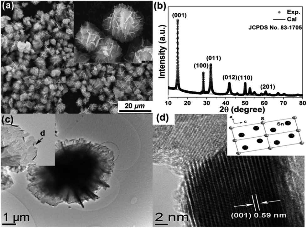 | ||
| Fig. 1 (a) SEM images of the as-prepared SnS2 3D hierarchical structures. (b) Corresponding observed (black dots) and calculated (black line) XRD patterns of the as-prepared sample. (c) TEM and (d) HRTEM image of the SnS2 nanosheet indicated by the arrow in (c) and schematic illustration of the crystal planes (inset). | ||
Photocatalytic activity
We evaluated the performance of the SnS2 sample as a photocatalyst for H2 production from 25 vol% of EtOH solution under different irradiation conditions with the presence of 1 wt% of Au as cocatalyst. Here, for a precise determination of the quantum efficiency, we characterized the 365 nm LED light and corrected the intensities of the 410 and 450 nm light relative to the 365 nm light; details are given in the discussion and in Fig. S9 in the ESI.† As depicted in Fig. 2, H2 generation was initiated as soon as purple (410 nm) or blue (450 nm) light irradiation was commenced, for which the H2 evolution rates were identical (∼100 μmol h−1). Since we used a catalyst loading of 50 mg, this corresponds to an impressive H2 production rate of ∼2 mmol g−1 h−1. However, the use of green light (500 nm) with a photon energy of 2.48 eV that is very close to the bandgap of SnS2 (∼2.2–2.4 eV)19 showed negligible evolution of H2. Interestingly, the SnS2 photocatalyst was also able to produce H2 under basic conditions (pH 11) with only a slightly reduced H2 evolution rate (∼65 μmol h−1). Moreover, the H2 evolution rates under visible light irradiation were even slightly better than that under UV irradiation (Fig. 2b). Since SnS2 may be subject to decomposition at low pH, successful operation of the photocatalyst under basic conditions indicates that long-term stability can be achieved. Stability tests indicate that the SnS2 sample was stable at least for 300 min at pH 7 and pH 11 (see Fig. S1 in ESI†). We have further estimated the apparent quantum efficiency (AQE) of the SnS2 photocatalyst as a function of the excitation wavelength, as shown in Fig. 2c. Although the efficiency dropped slightly as the emission wavelength increased, an impressive AQE of ∼4–5% was maintained under blue light (450 nm) irradiation. It should be noted that this high AQE is even better than some other popular visible light response photocatalysts, (for example, 1.9% for NiS/C3N4 under 440 nm irradiation).23 Since the specific surface area of the SnS2 sample was ∼6 m2 g−1 (Fig. S2 in ESI†), only 1/15 of that of similar structures reported by other groups,24,25 we conclude that the excellent photocatalytic performance cannot be directly related to the specific surface area, but to the unique surface structure of our SnS2 photocatalyst.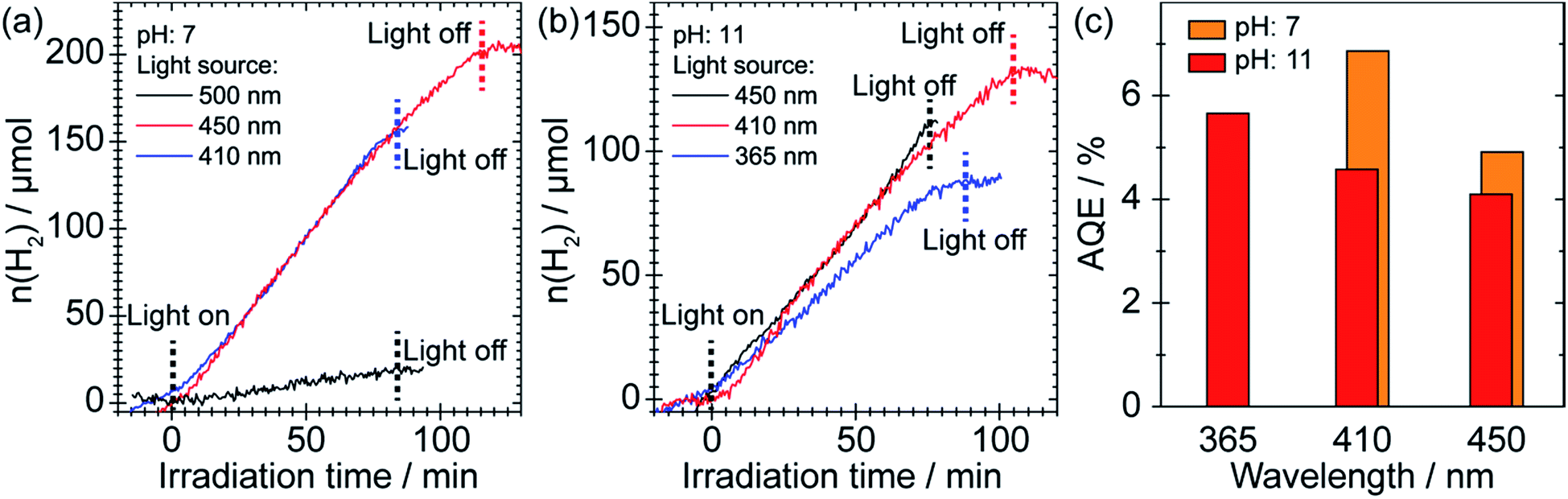 | ||
| Fig. 2 (a) and (b) Photocatalytic H2 evolution using 3D hierarchical structured SnS2 at pH 7 and 11, respectively. LED light sources with emission wavelengths of 365, 410, 450, and 500 nm were used to excite the material. A 25 vol% ethanol solution was used for each experiment. 1 wt% of Au was photodeposited on SnS2 as a cocatalyst. (c) Derived AQE at different pH and wavelength. AQE = 2n(H2)/n (incident photons). | ||
To obtain a better understanding of its excellent performance, UV-vis spectroscopy was used to reveal the optical properties of the as-prepared SnS2 in ethanol as shown in Fig. 3a. A sharp absorption peak is detected in the ultraviolet region at 257 nm. Such a peak has been reported for both SnS2 nanowires and nanosheets26–28 and its exact position may reflect the quantum size effects characteristic of the different nanostructures.29 Hence we can attribute this feature to the SnS2 phase. The band gap (Eg) is determined to be 2.04(5) eV, which is around 0.3 eV lower than most reported values thus far.19,30 In order to explain this finding, HRTEM was used to further explore the detailed structure of our SnS2 sample. In most areas of the nanosheets, clear lattice stripes with an interplanar distance of 0.316(2) nm are observed (Fig. 3b), which is consistent with the distance between parallel (100) planes or crystallographically equivalent (1![[1 with combining macron]](https://www.rsc.org/images/entities/char_0031_0304.gif) 0) planes of hexagonal SnS2.22 The corresponding fast Fourier transform (FFT) in the lower right inset of Fig. 3b resembles the diffraction pattern of a hexagonal phase along the [001] zone axis. This assignment is supported by the schematic illustration of the structure of hexagonal SnS2 viewed along the c-axis in the upper right inset of Fig. 3b, where the atomic arrangement resembles the lattice image. However, a different arrangement consisting of SnS2/SnS alternating regions is observed in many areas of the crystal (Fig. S3 and 3c). The measured interplanar distances in these areas after calibration are 0.316(2) and 0.188(2) nm, which are in agreement with the interplanar spacing of (100) planes of hexagonal SnS2 and (2) planes of orthorhombic SnS respectively, as shown in Fig. 3c. This is consistent with the XRD pattern in Fig. 1b, which on close inspection contains a weak 210 peak belonging to the SnS phase, as shown in Fig. S4.† The FFT of this lattice image resembles two superimposed diffraction patterns, one consistent with hexagonal SnS2 along the [001] zone axis (as shown in Fig. 3d, obtained by applying an array mask and keeping the masked area of the original FFT pattern obtained from the HRTEM image in the DigitalMicrograph software), and the other consistent with orthorhombic SnS along the [111] zone axis (as shown in Fig. 3e, also obtained by the same method). A clear crystallographic orientation relationship can be deduced from these FFT images such that (010)SnS2//(20)SnS and [001]SnS2//[111]SnS, as shown in Fig. 3c, since the spots 010 of SnS2 and 20 of SnS are exactly in a line with the central spot. We also note that the contrast between these two phases in the lattice image is obvious but the boundary is rather fuzzy, as indicated by the dashed lines in Fig. 3c. From the angle between the lattice fringes and the phase boundaries (∼30° in Fig. 3c) it can be deduced that the interfaces are comprised of (110) planes of hexagonal SnS2 and (2) planes of orthorhombic SnS. The interface is shown schematically in Fig. 3h. The fuzziness can be understood by noting that there is considerable lattice mismatch between the two different phases at the interface.
0) planes of hexagonal SnS2.22 The corresponding fast Fourier transform (FFT) in the lower right inset of Fig. 3b resembles the diffraction pattern of a hexagonal phase along the [001] zone axis. This assignment is supported by the schematic illustration of the structure of hexagonal SnS2 viewed along the c-axis in the upper right inset of Fig. 3b, where the atomic arrangement resembles the lattice image. However, a different arrangement consisting of SnS2/SnS alternating regions is observed in many areas of the crystal (Fig. S3 and 3c). The measured interplanar distances in these areas after calibration are 0.316(2) and 0.188(2) nm, which are in agreement with the interplanar spacing of (100) planes of hexagonal SnS2 and (2) planes of orthorhombic SnS respectively, as shown in Fig. 3c. This is consistent with the XRD pattern in Fig. 1b, which on close inspection contains a weak 210 peak belonging to the SnS phase, as shown in Fig. S4.† The FFT of this lattice image resembles two superimposed diffraction patterns, one consistent with hexagonal SnS2 along the [001] zone axis (as shown in Fig. 3d, obtained by applying an array mask and keeping the masked area of the original FFT pattern obtained from the HRTEM image in the DigitalMicrograph software), and the other consistent with orthorhombic SnS along the [111] zone axis (as shown in Fig. 3e, also obtained by the same method). A clear crystallographic orientation relationship can be deduced from these FFT images such that (010)SnS2//(20)SnS and [001]SnS2//[111]SnS, as shown in Fig. 3c, since the spots 010 of SnS2 and 20 of SnS are exactly in a line with the central spot. We also note that the contrast between these two phases in the lattice image is obvious but the boundary is rather fuzzy, as indicated by the dashed lines in Fig. 3c. From the angle between the lattice fringes and the phase boundaries (∼30° in Fig. 3c) it can be deduced that the interfaces are comprised of (110) planes of hexagonal SnS2 and (2) planes of orthorhombic SnS. The interface is shown schematically in Fig. 3h. The fuzziness can be understood by noting that there is considerable lattice mismatch between the two different phases at the interface.
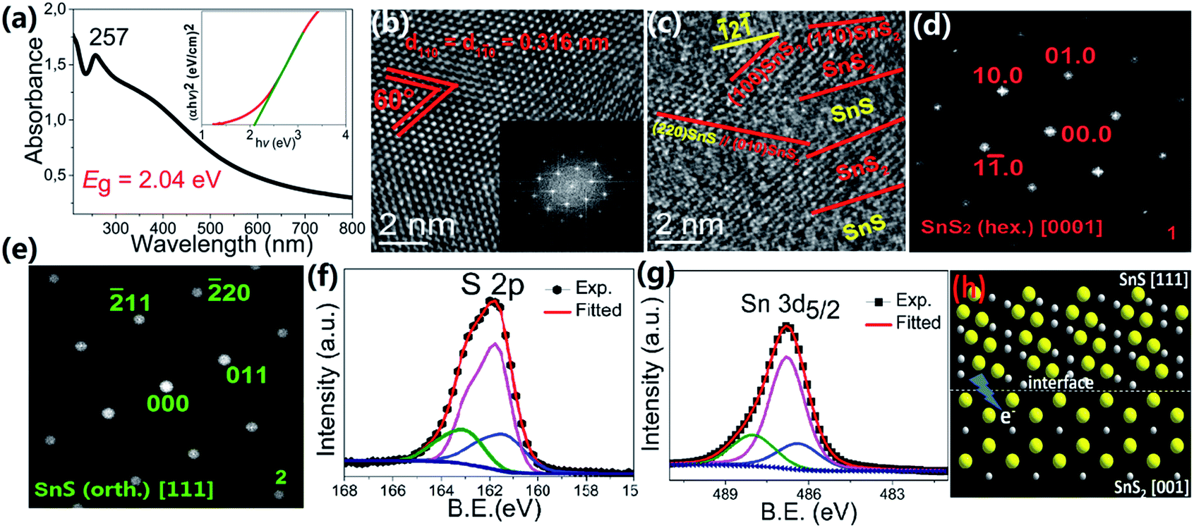 | ||
| Fig. 3 (a) UV-vis absorption spectra and plot of (αhν)2 against (hν) for the SnS2 spheres (inset). (b) HRTEM image of a typical nanoplate from a SnS2 sphere. The lower-right inset shows the corresponding FFT pattern; the upper-right inset illustrates the hexagonal structure viewed along the c axis. (c) HRTEM image of the nanoplate in different areas, which show alternating blocks of SnS2/SnS. (d, e) FFT images of the SnS2 and SnS phases, respectively, obtained by Fourier masking of the FFT pattern in (c). (f, g) XPS spectra of S 2p and Sn 3d core levels of the SnS2 sample. (h) Illustration of the SnS2/SnS interface based on analysis of the HRTEM images, where yellow and dark grey atoms represent S and Sn, respectively. | ||
X-ray photoelectron spectroscopy measurement
X-ray photoelectron spectroscopy (XPS) was used to reveal the chemical composition and oxidation states of our sample. Three contributions peaked at binding energies of 161.2, 161.7 and 162.9 eV are needed to fit the S 2p spectrum (Fig. 3f); the first two peaks, which account for 81.9% of the total S 2p spectral intensity, can be assigned to the S 2p doublets of SnS and SnS2, respectively.24 The higher binding energy peak, which accounts for 18.0% of the total S 2p spectral intensity, can be associated with the S2− in the sulfur deficient regions. A similar phenomenon is reported in many metal oxide systems with oxygen vacancies.31 The Sn 3d core level photoemission spectrum, presented in Fig. 3g, also needs to be fitted with three components to arrive at a satisfactory reconstruction of the spectrum. The components at 486.4 and 486.8 eV binding energy originate from Sn2+/4+ ions in SnS and SnS2, respectively.19,32 The third component at 488.0 eV, chemically shifted by 1.6 eV to higher binding energy, can be attributed to Sn in the sulfur deficient regions. This increased binding energy is surprising and we speculate that it may arise from the special type of Sn–Sn bonding at the SnS2/SnS interface. Research on CdS nanocrystal assemblies indicated that the distance between the transition metal is much smaller than in the metallic environment33 and consequently the valence electron charge is further away from the core level involved in the photoemission process and less able to screen the core hole. The SnS2/SnS superstructure can be viewed as a new kind of misfit structure, as illustrated in Fig. 3h, where the two layered phases contain Sn cations with different valence that are in close proximity to each other at the interface.34,35 This will lead to the creation of extra intra-band states due to the emergence of a Sn 5p bonding orbital, caused by Sn–Sn bonding. These induced impurity states will be more delocalized and their tails will reach into the gap, resulting in a smaller band gap that is more efficient for visible light absorption.33 On the other hand, in such a sandwich structure constructed by alternating nanoscale crystals, the Fermi energies of the two building blocks will align through electron transfer at the interface, as illustrated by the arrow in Fig. 3h. The formation of active centres will favour charge transfer across the interfaces and thus reduce the recombination rate of charge carriers, which improves the photocatalytic performance.36Finally, we extended our synthesis method to other hierarchical structures, by varying the metal chloride salt (FeCl2, CuCl2, or NiCl2·6H2O) and keeping all the other reaction conditions unchanged (details are given in Table S1†). For example, well organized CuS flowers can be synthesized on a large scale (Fig. 4a). Fig. 4b shows that these spheres have a hollow structure where the nanoplatelet building blocks are loosely packed and cross each other. Interestingly, FeS2 shows a different superstructure built from several bigger intersectional rough “petals” with a mean edge length of ∼5 μm (Fig. 4d). Fig. 4c and f, show the XRD patterns for CuS and FeS2 respectively. All peaks can be well indexed with JCPDS no. 03-0724 (hexagonal CuS), and 71-2219 (pyrite FeS2), with refined lattice parameters of a = 3.7903(2) Å, c = 16.3601(3) Å, γ = 120° (space group P63/m) for CuS, and a = 5.4346(1) Å, α = 90° (space group Pa) for FeS2. High purity Ni3S4 microspheres, a promising anode material for lithium ion batteries,37 were also synthesized using the same method, as shown by the SEM images in Fig. S5a and b† and by the fitted XRD patterns in Fig. S5c.† Furthermore, we have extended this method for the synthesis of mixed phase structures. For example, Fe7S8, which is a ferrimagnetic material with a high Curie temperature, can be added to the paramagnetic FeS2 phase by changing the reaction conditions slightly (Fig. S5f†). The hierarchical structure was retained perfectly, as shown in Fig. S5d and e,† and the sample showed strong magnetism at room temperature (Fig. S5e†). This would make the material much easier to recycle after use as a photocatalyst or in energy storage applications. Surface modification, which can provide a stable protective layer or facilitate charge transfer for the core material, was also explored here using the same strategy. Carbon was chosen as the coating layer to modify CuS as a representative example due to its low activity and high abundance. The fitted XRD pattern of the carbon-coated CuS sample is shown in the inset of Fig. 4g, from which we can see that all diffraction peaks can be indexed to the hexagonal CuS phase. An extra, broad feature centered at ∼25° was observed and can be attributed to amorphous carbon. SEM and low magnification TEM images (Fig. 4g and h) show that the as-prepared carbon-coated CuS product adopts a similar flower-like structure to the other samples, but assembled from a larger number of nanosheets. The thickness of these sheets decreased to only ∼10 nm. Compared with bare CuS, the dispersity and structural stability of carbon-coated CuS improved significantly. HRTEM images (Fig. 4i) taken at the edge of an ultrathin sheet showed that the CuS crystal was covered by a layer of amorphous carbon with a thickness of ∼3–5 nm. Clear lattice fringes were observed in the core material with interplanar spacings of 0.326(3) and 0.319(9) nm, which agree well with the d-spacings of the (100) and (101) planes of hexagonal CuS, respectively. The angle between these two planes was measured to be 74.5°, in exact agreement with the angle calculated using the unit cell parameters obtained from our XRD measurement.
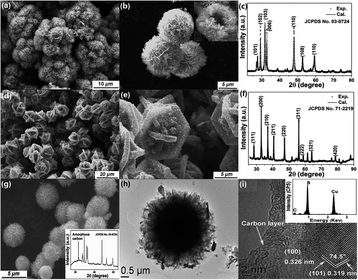 | ||
| Fig. 4 SEM images of the as-prepared CuS (a and b), and FeS2 (d and e) 3D hierarchical structures. (c) and (f) are the corresponding observed (black data points) and calculated (black line) XRD patterns of the as-prepared samples. (g) SEM and (h) TEM images of carbon coated CuS; the corresponding XRD pattern is shown in the inset to (g). (i) HRTEM image of a CuS@C nanosphere showing coating with an amorphous carbon layer; the inset shows the corresponding EDS spectrum. | ||
Formation mechanisms
To understand the formation mechanisms of our transition metal sulfide 3D hierarchical structures, we produced samples with different reaction times, using CuS as an example. Samples were collected and characterized after reaction times of 0, 0.3, 1, 2, 4, and 8 h, while all the other reaction conditions were kept the same as in the synthesis of CuS described in the Experimental section. The structural evolution process is in consistent with a typical two-step crystal growth mechanism in solution, where fast nucleation and self-assembly of primary nanoparticles is followed by a subsequent Ostwald ripening process. As shown in Fig. S6a(2),† no solid products were obtained if the reaction was stopped immediately when the temperature reached 180 °C. However, the colour of the solution changed from green to black and finally back to green Fig. S6a(3),† again after one day. This may indicate the formation of an unstable complex between CuCl2 and the solvent (ethanol + CS2) during the heating process. After only 0.3 h (the autoclave was taken out of the oven and cooled in air), flower structures composed of nanosheets started to form and remained the dominant morphology. Many scattered free particles with rough surfaces were also apparent, as shown by the arrows in Fig. S6b.† The magnified SEM image of a single flower structure is displayed in Fig. 5b and demonstrates that the spheres are assembled from tens of rounded petal-like structures of similar sizes, along with free-standing particles. A SEM image of the cross-section of one sphere indicated a hollow structure and the insertion of particles in the flower wall (Fig. S6b†). The corresponding elemental mapping (Fig. S6c†) suggested that Cl, O, and C were uniformly distributed in the flower along with the expected Cu and S, which is consistent with the corresponding energy dispersive X-ray (EDS) spectrum (Fig. S8†). The sample collected after a reaction time of 0.3 h but cooled down inside the oven (taking ∼12 h from 180 °C to room temperature) consisted of well developed flower-like structures; no scattered particles were observed (Fig. S8b†). The magnified SEM image of this structure reveals that it is assembled from hundreds of thin nanosheets with smooth surfaces and larger sizes compared to the building blocks shown in Fig. S6b.† When the reaction was allowed to proceed for 1 h (Fig. S8c†), the final morphology remained unchanged but the number of building blocks decreased significantly. Both the EDS spectra and elemental mappings were similar to those of the quickly quenched sample. Prolonged reaction times (2, 4, 8, and 24 h) only led to a further decrease in the number of building blocks and an increase in thickness of the nanosheets, as shown in Fig. 5d, e and S8c, d, and f.† In addition, only Cu and S remained in these products. The size of the flower-like structures did not change significantly during this process. Based on the above observations, a probable evolution process that is similar to the structure of real flowers is schematically illustrated in Fig. 5a. First, nucleation occurs within an extremely short time once the concentration of the solute reaches saturation conditions,29 and larger crystals are subsequently formed at the expense of the smaller ones because the solubility difference between relatively larger and smaller particles, which grows according to the Gibbs–Thomson law.38,39 In addition, because of the excellent solubility of CS2 in ethanol, the rapid decomposition of CS2 in the heat treatment process leads to the formation of numerous H2S gas bubbles, which serve as soft temsheets for the self-assembly.40 The freely scattered nanoparticles aggregate around these bubbles and form the final flower-like structures. A variety of forces, such as van der Waals attraction, attractive depletion forces, and Coulomb forces between surface charges or electric dipoles may be involved in the self-assembly process.15 Ostwald ripening dominates the subsequent evolution as the nanosheets undergo a structural modification. Specifically, Ostwald ripening of 2D islands (nuclei of new monolayers) and the capture of adatoms on the surface by the holes (incomplete regions of 2D islands) result in a smoother surface and increased thickness to achieve the minimal total surface free energy.41,42 | ||
| Fig. 5 (a) Schematic illustration of the formation of 3D CuS flower-like spheres. (b) SEM image of CuS prepared with a reaction time of 0.3 h and quenched quickly, and SEM images of samples obtained after reaction times of (c) 1 h, (d) 2 h, and (e) 8 h. | ||
Based on the elemental analysis, we can conclude that a precursor consisting of S, Cu, Cl, C, and O, rather than CuS, is formed in a short reaction time (less than 1 h). It has been proven that CS2 can bond with transition metals to form a wide variety of complexes. For example, CS2 can bond with the transition metal through a sulfur atom with the CS2 ligand acting as a Lewis base by donating a lone pair of electrons from the 1πg (HOMO) orbital to the corresponding vacant metal orbital (η2-end-on coordination). Meanwhile, the transition metal atom can also bond with a carbon atom by π-back donation from the metal atom to the CS2 ligand (η2-side-on coordination).43,44 This can be indirectly proven by the changing solution color and by XRD patterns. The XRD patterns of samples collected after 0.3 h and 1 h only exhibited weak, broad peaks due to the low crystallinity of the precursor (Fig. 6). Longer reaction times lead to the rapid decomposition of CS2 and sulfidisation of the precursor by the resulting H2S gas. This can be seen from the much sharper XRD peaks measured after a reaction time of 2 h (Fig. 6), where all the peaks belonging to hexagonal CuS are observed. A similar evolution process was previously found for the synthesis of PbS architectures, where the Pb–S–tartaric acid precursors were formed first and then oxidized by the yielding H2S gas.45
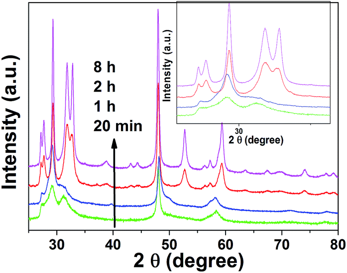 | ||
| Fig. 6 XRD patterns of the as-synthesized CuS superstructures with reaction times of 0.3 h, 1, 2, and 8 h. | ||
Conclusions
In summary, we propose an easy and general method for the synthesis of transition metal sulfide 3D hierarchical structures. Our study of SnS2 indicates that the band gap as well as the heterojunctions can be adjusted by the introduction of sulfur vacancies, which significantly improve the visible light-induced photocatalytic H2 production due to enhanced light absorption and charge separation. This suggests a new route toward efficient photocatalysts without doping. Finally, a formation mechanism based on a self-assembly process is proposed for the hierarchical structures.Acknowledgements
This work is funded by the Netherlands Organization for Scientific Research (NWO-CW: 712.011.003). We also thank the Danish Strategic Research Council, the Carlsberg Foundation, and the National Natural Science Foundation of China (Project No: 21503257) for financial support. The authors thank Jacob Baas for technical support.References
- Y. Li, Z. Y. Fu and B. L. Su, Adv. Funct. Mater., 2012, 22, 4634–4667 CrossRef CAS.
- H. B. Yao, H. Y. Fang, X. H. Wang and S. H. Yu, Chem. Soc. Rev., 2011, 40, 3764–3785 RSC.
- H. B. Wu, H. Pang and X. W. Lou, Energy Environ. Sci., 2013, 6, 3619–3626 CAS.
- J. Y. Duan, G. Y. Mou, S. Zhang, S. Wang and J. G. Guan, J. Mater. Chem. A, 2015, 3, 14686–14695 CAS.
- H. Wang, K. Dou, W. Y. Teoh, Y. Zhan, T. F. Hung, F. Zhang, J. Xu, R. Zhang and A. L. Rogach, Adv. Funct. Mater., 2013, 23, 4847–4853 CAS.
- J. S. Chen, Y. L. Tan, C. M. Li, Y. L. Cheah, D. Y. Luan, S. Madhavi, F. Y. C. Boey, L. A. Archer and X. W. Lou, J. Am. Chem. Soc., 2010, 132, 6124–6130 CrossRef CAS PubMed.
- D. Fan, P. John Thomas and P. O'Brien, J. Am. Chem. Soc., 2008, 130, 10892–10894 CrossRef CAS PubMed.
- C. di Giovanni, W.-A. Wang, S. Nowak, J.-M. Grenèche, H. Lecoq, L. Mouton, M. Giraud and C. Tard, ACS Catal., 2014, 4, 681–687 CrossRef CAS.
- Z. Jiao, T. Chen, J. Xiong, T. Wang, G. Lu, J. Ye and Y. Bi, Sci. Rep., 2013, 3, 2720 Search PubMed.
- R. Asahi, T. Morikawa, T. Ohwaki, K. Aoki and Y. Taga, Science, 2001, 293, 269–271 CrossRef CAS PubMed.
- W. Zhu, X. Qiu, V. Iancu, X.-Q. Chen, H. Pan, W. Wang, N. Dimitrijevic, T. Rajh, H. Meyer, M. Paranthaman, G. Stocks, H. Weitering, B. Gu, G. Eres and Z. Zhang, Phys. Rev. Lett., 2009, 103, 226401 CrossRef PubMed.
- C. Galeano, J. C. Meier, M. Soorholtz, H. Bongard, C. Baldizzone, K. J. J. Mayrhofer and F. Schüth, ACS Catal., 2014, 4, 3856–3868 CrossRef CAS.
- M. Liu, D. Jing, Z. Zhou and L. Guo, Nat. Commun., 2013, 4, 2278 Search PubMed.
- M. Liu, L. Wang, G. Lu, X. Yao and L. Guo, Energy Environ. Sci., 2011, 4, 1372 CAS.
- K. Miszta, J. de Graaf, G. Bertoni, D. Dorfs, R. Brescia, S. Marras, L. Ceseracciu, R. Cingolani, R. van Roij, M. Dijkstra and L. Manna, Nat. Mater., 2011, 10, 872–876 CrossRef CAS PubMed.
- Z. Bian, J. Zhu, J. Wang, S. Xiao, C. Nuckolls and H. Li, J. Am. Chem. Soc., 2012, 134, 2325–2331 CrossRef CAS PubMed.
- C. M. Parlett, K. Wilson and A. F. Lee, Chem. Soc. Rev., 2013, 42, 3876–3893 RSC.
- Z. Niu and Y. Li, Chem. Mater., 2014, 26, 72–83 CrossRef CAS.
- Y. C. Zhang, J. Li, M. Zhang and D. D. Dionysiou, Environ. Sci. Technol., 2011, 45, 9324–9331 CrossRef CAS PubMed.
- G. R. Bamwenda, S. Tsubota, T. Nakamura and M. Haruta, J. Photochem. Photobiol., A, 1995, 89, 177–189 CrossRef CAS.
- R. Su, R. Tiruvalam, A. J. Logsdail, Q. He, C. A. Downing, M. T. Jensen, N. Dimitratos, L. Kesavan, P. P. Wells, R. Bechstein, H. H. Jensen, S. Wendt, C. R. Catlow, C. J. Kiely, G. J. Hutchings and F. Besenbacher, ACS Nano, 2014, 8, 3490–3497 CrossRef CAS PubMed.
- J. W. Seo, J. T. Jang, S. W. Park, C. J. Kim, B. W. Park and J. W. Cheon, Adv. Mater., 2008, 20, 4269–4273 CrossRef CAS.
- J. Hong, Y. Wang, Y. Wang, W. Zhang and R. Xu, ChemSusChem, 2013, 6, 2263–2268 CrossRef CAS PubMed.
- Y. C. Zhang, Z. N. Du, K. W. Li, M. Zhang and D. D. Dionysiou, ACS Appl. Mater. Interfaces, 2011, 3, 1528–1537 CAS.
- Y. Lei, S. Song, W. Fan, Y. Xing and H. Zhan, J. Phys. Chem. C, 2009, 113, 1280–1285 CAS.
- X. Zhou, T. Zhou, J. Hu and J. Li, CrystEngComm, 2012, 14, 5627 RSC.
- M. Li, E. Liu, H. Hu, S. Ouyang, H. Xu and D. Wang, Int. J. Photoenergy, 2014, 2014, 1–7 Search PubMed.
- Y. T. Lin, J. B. Shi, Y. C. Chen, C. J. Chen and P. F. Wu, Nanoscale Res. Lett., 2009, 4, 694–698 CrossRef CAS PubMed.
- X. Zhou, L. Ma and Z. Feng, Chem. Lett., 2015, 44, 1113–1115 CrossRef CAS.
- L. A. Burton, D. Colombara, R. D. Abellon, F. C. Grozema, L. M. Peter, T. J. Savenije, G. Dennler and A. Walsh, Chem. Mater., 2013, 25, 4908–4916 CrossRef CAS.
- J. Wang, Z. Wang, B. Huang, Y. Ma, Y. Liu, X. Qin, X. Zhang and Y. Dai, ACS Appl. Mater. Interfaces, 2012, 4, 4024–4030 CAS.
- Y. C. Lu, C. Ma, J. Alvarado, N. Dimov, Y. S. Meng and S. Okada, J. Mater. Chem. A, 2015, 3, 16971–16977 CAS.
- H. Tong, N. Umezawa, J. Ye and T. Ohno, Energy Environ. Sci., 2011, 4, 1684–1689 CAS.
- S. Y. Hong, R. Popovitz-Biro, Y. Prior and R. Tenne, J. Am. Chem. Soc., 2003, 125, 10470–10474 CrossRef CAS PubMed.
- G. Radovsky, R. Popovitz-Biro, M. Staiger, K. Gartsman, C. Thomsen, T. Lorenz, G. Seifert and R. Tenne, Angew. Chem., Int. Ed., 2011, 50, 12316–12320 CrossRef CAS PubMed.
- Q. Li, C. Zhang, J. Ma, G. Wang and D. H. L. Ng, ChemCatChem, 2014, 6, 1392–1400 CAS.
- N. Mahmood, C. Zhang and Y. Hou, Small, 2013, 9, 1321–1328 CrossRef CAS PubMed.
- Z. P. Zhang, H. P. Sun, X. Q. Shao, D. F. Li, H. D. Yu and M. Y. Han, Adv. Mater., 2005, 17, 42–47 CrossRef CAS.
- G. Li, C. Li, H. Tang, K. Cao and J. Chen, Mater. Res. Bull., 2011, 46, 1072–1079 CrossRef CAS.
- X. W. Lou, L. A. Archer and Z. Yang, Adv. Mater., 2008, 20, 3987–4019 CrossRef CAS.
- A. Y. Kaminski and R. A. Suris, Appl. Surf. Sci., 1996, 104, 312–316 CrossRef.
- H. Zhang, Q. Zhu, Y. Zhang, Y. Wang, L. Zhao and B. Yu, Adv. Funct. Mater., 2007, 17, 2766–2771 CrossRef CAS.
- P. V. Yaneff, Coord. Chem. Rev., 1977, 23, 183–220 CrossRef CAS.
- K. K. Pandey, Coord. Chem. Rev., 1995, 140, 37–114 CrossRef CAS.
- G. Li, C. Li, X. Yang, H. L. Ng Dikon and H. Tang, Mater. Chem. Phys., 2011, 129, 1011–1019 CrossRef CAS.
Footnote |
| † Electronic supplementary information (ESI) available. See DOI: 10.1039/c5ta07283b |
| This journal is © The Royal Society of Chemistry 2016 |