
 Open Access Article
 This Open Access Article is licensed under a
 Creative Commons Attribution 3.0 Unported Licence
Molecular engineering of benzothienoisoindigo copolymers allowing highly preferential face-on orientations†
Marina
Ide
a,
Akinori
Saeki
*a,
Yoshiko
Koizumi
a,
Tomoyuki
Koganezawa
b and
Shu
Seki
 *ac
*ac
aDepartment of Applied Chemistry, Graduate School of Engineering, Osaka University, 2-1 Yamadaoka, Suita, Osaka 565-0871, Japan. E-mail: saeki@chem.eng.osaka-u.ac.jp; seki@moleng.kyoto-u.ac.jp
bJapan Synchrotron Radiation Research Institute, 1-1-1, Kouto, Sayo-cho, Sayo-gun, Hyogo 679-5198, Japan
cDepartment of Molecular Engineering, Graduate School of Engineering, Kyoto University, Nishikyo-ku, Kyoto 615-8510, Japan
First published on 31st August 2015
Abstract
Orientation of conjugated polymers is increasingly important in organic photovoltaics (OPV) to achieve high power conversion efficiency (PCE). The optimized orientation of conjugated backbones for photo-generated charge carriers in OPV devices is in contrast to organic semiconductor devices, demanding new strategies to control and realize face-on orientation of conjugated systems onto substrates. Here we report new conjugated polymers composed of electron-accepting benzothienoisoindigo (BTIDG), an asymmetric unit of isoindigo and thienoisoindigo. BTIDG was coupled with weakly electron-donating thiazolothiazole or benzobisthiazole, concurrently leading to moderate optical band gaps (1.41–1.52 eV) and the highest occupied molecular orbital (−5.35 to −5.50 eV). The alkylthiophene spacer between BTIDG and the donor unit provided a marked control over the orientation of polymers, among which the degree of face-on orientation as high as 95% was revealed by grazing incidence X-ray diffraction. The maximum PCE was improved up to 4.2% using the system with [6,6]-phenyl-C71-butyric acid methyl ester (PC71BM). We present a useful basis on the structure (orientation)–property (OPV output) relationship to lay down new guidelines for the design of efficient solar cell materials.
Introduction
A low bandgap polymer (LBP) constituting of electron donor and acceptor units is expected to create an efficient organic photovoltaic device (OPV),1–4 due to its wide photoabsorption and the deep highest occupied molecular orbital (HOMO). Thienoisoindigo (TIDG), analogous to isoindigo (IDG),5–7 is a comparatively new electron acceptor which we8 and other groups9,10 have reported in 2012–2013. Replacing the phenyl of IDG by thiophene led to a more planar π-plane and stronger electron accepting ability than IDG. However, TIDG resulted in an excessively narrow optical bandgap (Eoptg, 1.0–1.1 eV) in conjugation with the benchmark donors (benzodithiophene and cyclopentadithiophene).8 An unsatisfactory PCE of 1.4% was obtained as the best value for the blend of [6,6]-phenyl-C61-butyric acid methyl ester (PC61BM) and fluorene-TIDG polymer (Eoptg = 1.6 eV).11 In addition to their mismatches in energy alignment, we have identified the limiting factors of photovoltaic performance, i.e. the short exciton lifetime, the loss via bulk charge recombination, and unfavorable orientation/morphology partly associated with insufficient solubility.11 Therefore, simultaneous control of these factors through molecular engineering or processing is a crucial prerequisite towards boosting the PCE of TIDG-based polymers; however this is a challenging theme shared by all disciplines.One of the synthetic routes to the TIDG unit we have reported for the first time is the dimerization of mono-keto and di-keto precursors in acetic acid, the former of which was prepared by reacting the di-keto precursor with hydrazine reagent followed by Wolff–Kishner type reduction.8 Inspired by this quantitative and heterotic dimerization scheme, we attempted the synthesis of half-TIDG and half-IDG units from their relevant two precursors. This would bring moderate electron accepting nature with a good solubility as a result of its asymmetric half-distorted π-plane. In the course of research, Chen and Fréchet et al.12 reported this benzothienoisoindigo (BTIDG)-based polymer synthesized by an almost similar route and demonstrated a large improvement of PCE (4.7%) for the terthiophene-BTIDG copolymer. Notably, they realized selective manipulation of edge-on or face-on orientation of polymers by controlling the backbone planarity (IDG or BTIDG) suitable for field-effect transistors (FETs) or OPV devices, respectively. However, the high-performing BTIDG copolymer still includes some portions of edge-on contribution, suggestive of extra room for enhancing the portion of face-on orientated polymer crystallites where considerable improvement has been reported in both charge carrier transport and overall PCE of OPV devices.13
In this work, we synthesized novel BTIDG-based copolymers in combination with benzobisthiazole (BBTz)14,15 or thiazolothiazole (TzTz),16,17 where BBTz and TzTz are normally electron acceptors but used as weak donors18–20 against BTIDG. This molecular design is intended to provide both optimal Eoptg (ideally 1.37–1.45 eV from the calculation)21 and HOMO levels. Furthermore, we exemplified the synergetic impact of the alkylthiophene spacer on the control of polymer orientation and OPV output.
Results and discussion
Optical and electrochemical properties
The brominated BTIDG monomer (9) and alkylthiophene-BTIDG monomer (11) were synthesized according to the route of Scheme 1. Synthesis and characterization of the compounds (1)–(8) including 1H NMR and mass spectroscopy data are provided in the ESI and Scheme S1.† BTDTG-based copolymers were polymerized by the Stille coupling reaction (Scheme 2).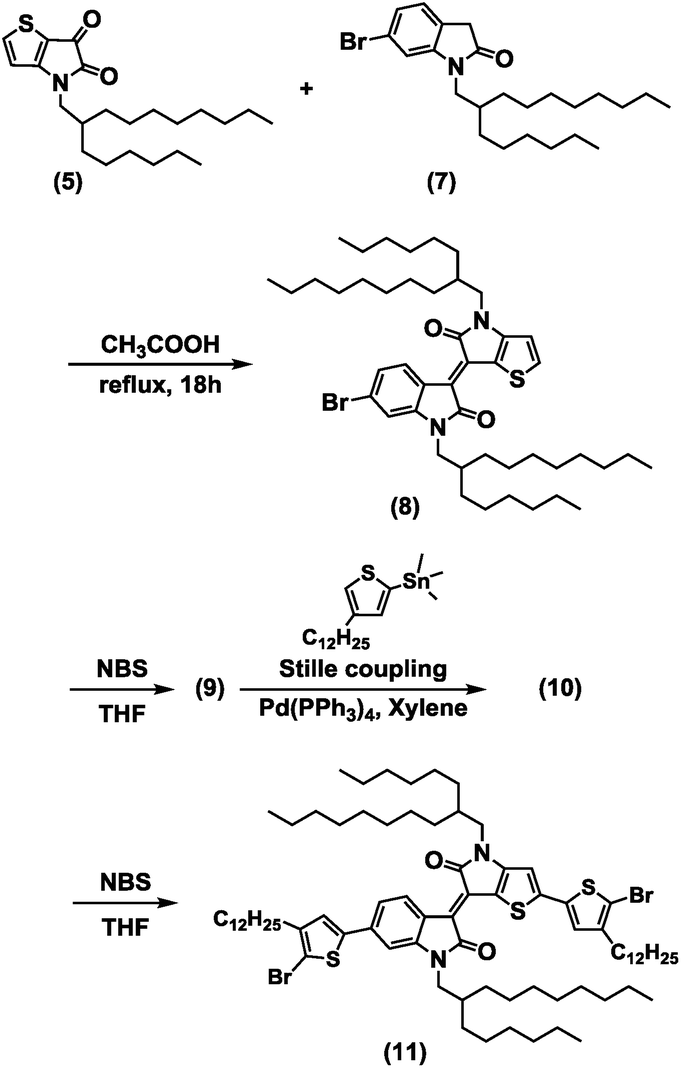 | ||
| Scheme 1 Synthetic procedure of the BTIDG unit. Those of (5) and (7) are provided in the ESI.† | ||
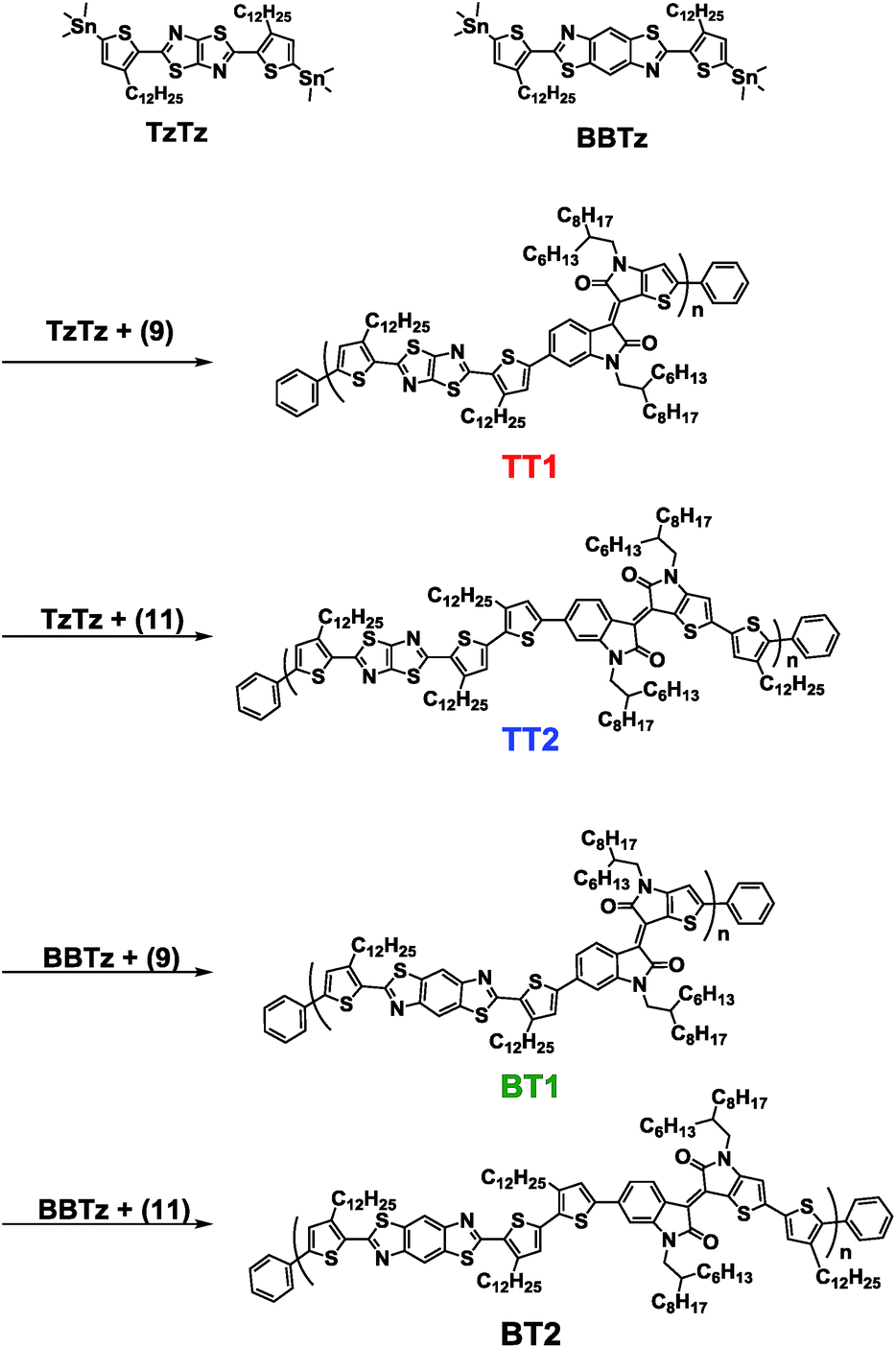 | ||
| Scheme 2 Synthesis of BTIDG polymers. | ||
Fig. 1a shows the chemical structures of BTIDG-based copolymers: TT1, TT2, BT1, and BT2, in which the number (1 or 2) represents the length of the alkylthiophene spacer (thiophene or bithiophene). Electronic absorption spectra of BTIDG polymers were measured in chloroform solution (Fig. 1b) and thin film (Fig. 1c). The BTIDG polymers indicate the absorption edges at ca. 820–880 nm corresponding to the Eoptg of 1.41–1.52 eV (Table 1). These Eoptg values are finely tuned to the aforementioned ideal value for single cell OPV polymers,21 which is a notable advantage over the previous near-infrared absorbing TIDG polymers. In addition, the weight-averaged molecular weights (Mw) of BTIDG polymers are as high as 127–231 kg mol−1 (Table 1) except for TT1 (32 kg mol−1), which is much higher than those of the previous TIDG polymers (15–87 kg mol−1).8 This is because the solubility was significantly improved by virtue of the long linear alkyl chains of the thiophene spacer and branched ones of asymmetric BTIDG.
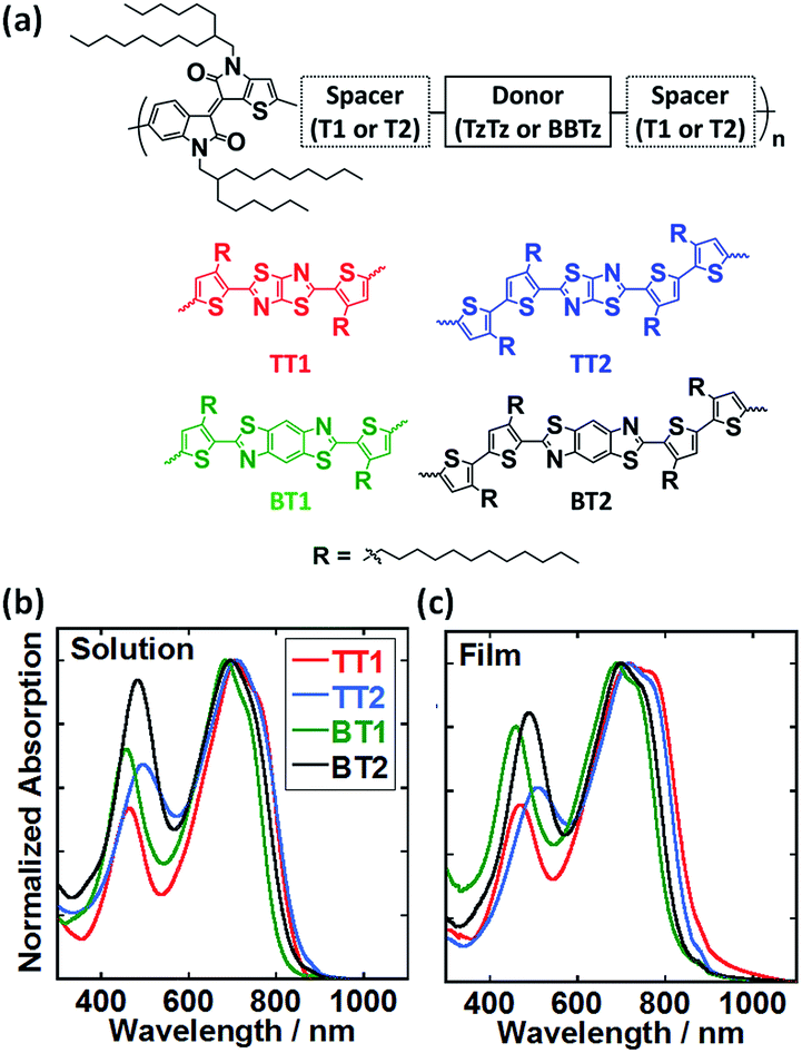 | ||
| Fig. 1 (a) Chemical structures of BTIDG polymers. (b) Electronic absorption spectra of TT1 (red line), TT2 (blue line), BT1 (green line) and BT2 (black line) in chloroform solution at room temperature, respectively. (c) Electronic absorption spectra of TT1, TT2, BT1 and BT2 as films dropcast from chloroform solution. | ||
| Polymer | M w/kg mol−1 (PDI) | HOMOa/eV | LUMOb/eV | λ max /nm | E optg /eV |
|---|---|---|---|---|---|
| a Determined by PYS of drop-cast films. b HOMO + Eoptg. c In film states. d Determined from the onset of the electronic absorption spectra in film states. | |||||
| TT1 | 32 (1.7) | −5.35 | −3.94 | 718 | 1.41 |
| TT2 | 127 (3.5) | −5.43 | −3.98 | 719 | 1.45 |
| BT1 | 142 (2.1) | −5.50 | −3.98 | 690 | 1.52 |
| BT2 | 231 (3.9) | −5.41 | −3.92 | 699 | 1.49 |
Photoelectron yield spectroscopy (PYS, Fig. S1†) was performed to estimate the HOMO levels of polymer films, giving slightly varying HOMOs (−5.35 to −5.50 eV) and almost identical lowest unoccupied molecular orbitals (LUMO, −3.92 to −3.98 eV). These HOMOs are indeed much deeper than those of our previous TIDG polymers (HOMO: −4.7 to −5.4 eV, LUMO: −3.8 eV),8 while the LUMO–LUMO offsets between polymer and PCBM (−4.2 eV)22 became close to or even less than the empirically required minimum value (0.3 eV).23,24
Electron withdrawing nature of the BTIDG unit is clearly evident from the density functional theory (DFT) calculation shown in Fig. S2.† The LUMO is localized on the BTIDG unit, while the HOMO is spread over the polymer backbone of the donor (BT or TT), spacer (thiophene), and BTIDG, similar to the TIDG8 and IDG25 polymers. Thanks to the inherently high coplanarity and low LUMO, TIDG-thiophene and -naphthalene copolymers have uncovered ambipolar charge transport (μh = 0.18 cm2 V−1 s−1 and μe = 0.03 cm2 V−1 s−1)26 and ultrahigh hole mobility up to 14 cm2 V−1 s−1,27 respectively. In addition, nonbonding Coulomb interactions arising from the difference in the electronegativity of the sulfur atom of spacer thiophene and the nitrogen atom of TTz and BBTz could facilitate coplanarity of the π-conjugated polymer backbone. This is supported by the DFT calculation exhibiting that the total energy of N⋯S conformation is 7 kJ mol−1 lower than that of S⋯S conformation (Fig. S3†), consistent with that of chalcogen (S⋯O)26 and N⋯S interactions28 reported previously.
Polymer orientation and hole mobilities
Polymer orientation in pristine and PC61BM blend films was characterized by two-dimensional grazing-incidence X-ray diffraction (2D-GIXRD) shown in Fig. 2. Thin spin-coated pristine films (ca. 60 nm) contained an intense tail of direct X-ray overlapping the weak diffraction of polymer in the out-of-plane low angle diffraction region. This hampers the quantitative analysis of face-on and edge-on orientation (Fig. S4†), and thus the thick pristine films (ca. 1 μm) prepared by drop-casting were evaluated. It needs to be mentioned, though, that the π–π stacking distance and face-on/edge-on orientations were mostly unchanged between spun-coat and drop-cast films. The blend films were prepared in the same way with the optimal OPV device fabrication (vide infra). Surprisingly, all of the pristine polymers indicate profound face-on orientation with negligibly small edge-on peaks. The π–π stacking distances are moderate, ranging from 3.57 Å for BT1 to 3.67 Å for TT2 (Table 2). Although the π–π stacking distances did not display obvious variations by the molecular structure, the lamellar packing distances were rationally increased from the mono-thiophene spacer (24.8 Å for both TT1 and BT1) to the bis-thiophene one (26.1 Å for TT2 and 25.4 Å BT2).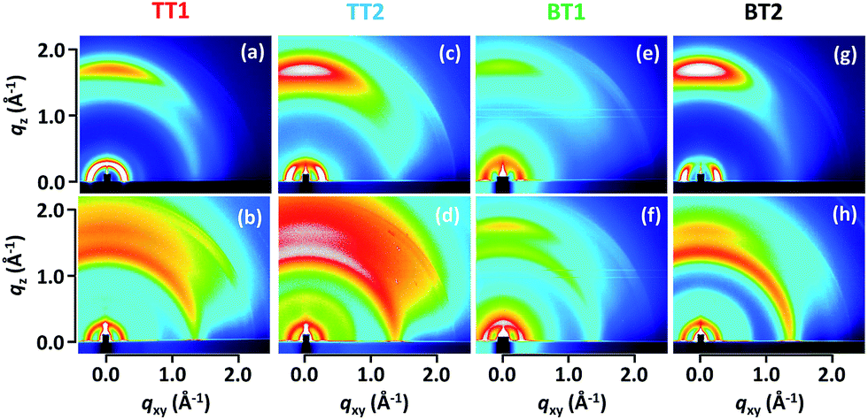 | ||
| Fig. 2 2D-GIXRD patterns of pristine TT1 (a), TT2 (c), BT1 (e) and BT2 (g) drop-cast on the ITO substrate. (b), (d), (f) and (h) are the patterns of optimal OPV devices (polymer and PC61BM blends). | ||
| Film (p/n ratio) | π–πa/Å | ILb/Å | R face-on | μ h/10−5 cm2 V−1 s—1 |
|---|---|---|---|---|
| a Calculated from the (010) peaks in the out-of-plane direction. b Interlamellar distance calculated from the (100) peaks in the in-plane direction. c Calculated by Iip/(Iip + Iop). | ||||
| TT1 | 3.64 | 24.8 | 67% | 1.0 |
TT1![[thin space (1/6-em)]](https://www.rsc.org/images/entities/char_2009.gif) :PC61BM (1:1) :PC61BM (1:1) |
3.64 | 24.8 | 40% | 6.8 |
| TT2 | 3.67 | 26.1 | 80% | 5.9 |
|
TT2:PC61BM (1:2) |
3.71 | 26.1 | 73% | 10 |
| BT1 | 3.57 | 24.8 | 93% | 0.18 |
|
BT1:PC61BM (1:2) |
3.54 | 23.7 | 68% | 4.9 |
| BT2 | 3.66 | 25.4 | 95% | 120 |
|
BT2:PC61BM (1:2) |
3.64 | 24.8 | 75% | 12 |
The ratio of face-on orientation (Rface-on in %) was evaluated by Iip/(Iip + Iop), where Iip and Iop are the peak intensities of (100) diffraction in the in-plane and out-of-plane directions, respectively (Fig. S5†). It should be noted that Rface-on is an approximation of face-on fraction in the XRD-active crystalline part,17,29 and thus Rface-on is not directly associated with the crystallinity of polymer. Besides, out-of-plane diffraction tends to appear with higher intensity than its actual composition, due to the combination of the thin film geometry and the constraint of one axis to the sample plane in the polar figure.30 By taking these into account, Rface-on evaluation in this study is supposed to be slightly underestimated, since the out-of-plane diffraction at the small scattering vector attributed to edge-on orientation could be stronger than is the actual case. As listed in Table 2, pristine BT2 shows a pronounced Rface-on as high as 95% (the ratio of face-on to edge-on, Iip/Iop is ca. 19). To the best of our knowledge, this is the top-class preferential face-on orientation reported so far in OPV polymers. Examples of high Rface-on polymers are thiazolothiazole (91%)17 and dicarboximide-dithiophene (PBTI3T, 93%, face-on:edge-on = 14)31 polymers. The pioneering LBPs of benzodithiophene (BDT)-thienopyrroledione (PBDTTPD)32,33 and BDT-thienothiophene (PTB7 and PBDTTT-C-T)34–36 of which the PCE exceeded 6–7% in 2010 also have high face-on orientation. We extracted an Rface-on of 94% for pristine PTB7 from its 2D-GIXRD image (Fig. S5†),37 corroborating the high face-on orientation of the successful polymer. Other early LBPs such as carbazole-benzothiaziazole (PCDTBT)38 and cyclopentadithiophene-benzothiaziazole (PCPDTBT)39 also indicate the face-on preferred 2D-GIXRD images along with rather amorphous features. Since the face-on orientation is advantageous for vertical charge transport in OPV cells,13,17,31 recent development of high performance LBPs is directed to control the polymer orientation as well as bandgap engineering. The second highest Rface-on of 93% was found for BT1 followed by TT2 (80%) and TT1 (67%).
Due to the complicated factors affecting the polymer orientation, a rational molecular design of face-on polymers remains poorly understood. Solubility, shape of solubilizing alkyl chains (branched one is likely more favorable for face-on than linear one), and the length of alkyl chains have been supposed as the premiere factors that control polymer orientation. In the present study, the sizes of the π-plane (BT > TT) and spacer (bithiophene:2 > thiophene:1) were found to have an impact on improving face-on orientation. In sharp contrast, mixing with PC61BM significantly decreased the face-on orientation. The similar trend appeared in all blend films, where Rface-on dropped by 10–20% (Table 2). For instance, the most face-on-preferred BT2 indicates a Rface-on of 75% in the PCBM blend, accompanied by a decrease of diffraction intensity.
Hole mobilities (μh) of BTIDG polymers and their blends with PC61BM were measured by using a space-charge limited current (SCLC) technique40 (Table 2 and Fig. S6†). Remarkably, the most face-on-orientated pristine BT2 demonstrated the highest μh of 1.2 × 10⁻³ cm2 V−1 s−1, while the other polymers gave 2–3 orders of magnitude smaller values (10−5 to 10−6 cm2 V−1 s−1). The BT2:PC61BM blend film showed a μh of 1.2 × 10⁻⁴ cm2 V−1 s−1 decreased by one order of magnitude; however, this is still higher than the other polymer blends (10−4 to 10−5 cm2 V−1 s−1). Despite the reduced diffraction intensities upon mixing with PC61BM, the π–π stacking and lamellar packing distances were mostly unchanged, indicative of no intercalation into the polymer crystallites. Interestingly, the μh values of PC61BM-blended TT1, TT2, and BT1 are comparable to or even higher than those of pristine polymers, regardless of the deceased Rface-on. Although the cause of the enhanced μh in the blend films is unclear, this might merit the OPV performance which prefers a high μh in the vertical direction.
Solar cell performance
Fig. 3a shows current–voltage curves of normal cell OPV (PEDOT:PSS/active layer/Ca/Al). The active layers were prepared from chlorobenzene (CB) solution with a 3 vol% solvent additive of either 1,8-diiodooctane (DIO) or 1-chloronaphthalene (CN). We have examined the p/n blend ratio (1:1 ∼ 1:5), film thickness, and thermal annealing effect (80, 120, and 150 °C). The optimal device parameters are summarized in Table 3, where the best blend ratio depends on the polymer (from 1:1 to 1:3) and no thermal annealing is preferred for all the polymers. The other low-performing device outputs are listed in Tables S1–S4.† Except for the low PCE of TT1 (0.60%), TT2, BT1, and BT2 indicated comparable PCEs from 3.3 to 3.7%. The best PCE of 3.74% (average 3.47%) was achieved for BT2:PC61BM = 1:2 with an open-circuit voltage (Voc) of 0.62 V, a Jsc of 10.07 mA cm−2, and a fill factor (FF) of 0.66. The external quantum efficiency (EQE) spectra of TT2, BT1, and BT2 shown in Fig. 3b present almost identical features corresponding to the superposition of polymer and PC61BM absorption spectra. The calculated Jsc (= Jcalcsc) from the EQE spectra is in excellent agreement with the Jsc under 1 sun (Table 3), indicative of the appropriate evaluation. The lowest-performing TT1 shows a suppressed EQE spectrum and low Jsc, arising from the lowest face-on orientation (Rface-on = 40%) and molecular weight.
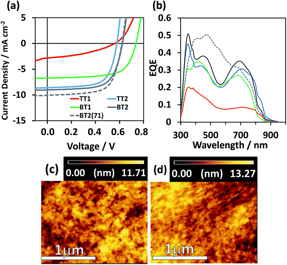 | ||
| Fig. 3 (a) J–V curves and (b) EQE spectra of the best-performing OPV devices. AFM topology images (2 × 2 μm) of (c) BT2:PC61BM = 1:2 and (d) BT2:PC71BM = 1:2. The scale bar at the bottom is 1 μm. | ||
| Blenda | p/n ratiob | L /nm | PCEd (average)/% | V oc/V | J sc/mA cm−2 | FF | J calcsc/mA cm−2 (Jsc/Jcalcsc)e |
|---|---|---|---|---|---|---|---|
|
a Normal cell structure (PEDOT:PSS/active layer/Ca/Al). The active layers were fabricated by chlorobenzene solution with 3 v/v % DIO or CN. No thermal annealing was applied for the active layer.
b In weight% fraction.
c Thickness of the active layer.
d The maximum PCE. The value in the brackets is an average PCE over at least 5 devices.
e The calculated Jsc by integrating the EQE spectrum. The value in the brackets is Jsc/Jcalcsc.
|
|||||||
|
TT1:PC61BM |
1:1 |
79 | 0.60 (0.48) | 0.56 | 2.83 | 0.38 | 2.85 (0.99) |
|
TT2:PC61BM |
1:2 |
150 | 3.40 (3.22) | 0.58 | 8.54 | 0.69 | 7.90 (1.08) |
|
BT1:PC61BM |
1:3 |
84 | 3.29 (3.21) | 0.73 | 6.72 | 0.67 | 6.74 (1.00) |
|
BT2:PC61BM |
1:2 |
89 | 3.74 (3.47) | 0.62 | 9.01 | 0.66 | 8.68 (1.04) |
|
BT2:PC71BM |
1:2 |
90 | 4.18 (3.92) | 0.62 | 10.07 | 0.67 | 10.04 (1.00) |
The film morphologies observed by atomic force microscopy (AFM) are almost similar (Fig. 3c and d and S7†). Voc is presumably proportional to the energy difference between the HOMO of the p-type polymer and the LUMO of n-type fullerene with an energy loss ranging from 0.8 to 1.3 eV.41 The highest Voc of 0.73 V was obtained for BT1 (HOMO = −5.50 eV), while those of other polymers having the almost same HOMO of −5.35 to −5.43 eV were ca. 0.56–0.62 V, consistent with 0.1 V lower HOMOs.
To improve the PCE of the best-performing BT2-based OPV cell, PC61BM was replaced by PC71BM which has higher absorption in the visible region than the former. As a result, BT2:PC71BM boosted the PCE to 4.18% (average 3.92%), due to the increased Jsc of 10.1 mA cm−2 without sacrifices of Voc (0.62 V) and FF (0.67). The film morphologies of BT2:PC61BM and BT2:PC71BM were almost identical as visualized in the AFM images of Fig. 3c and d. We also examined a thicker film of BT2:PC61BM, because high PCEs of 9–10% were achieved for thick active layers (ca. 300 nm) composed of crystalline polymers.13,42,43 The PCE of 300 nm-thick BT2:PC61BM was 3.51%, being equal to the 120 nm-thick film (3.50%). Despite the identical Voc (0.61 V), the Jsc and FF of the 300 nm-thick film were increased to 13.38 mA cm−2 and decreased to 0.43, respectively, indicative of the typical trade-off relationship.17 In the manufacturing stage of OPV cells via high-throughput inkjet printing, a polymer without strong thickness dependence is highly favorable44 in which BT2 could be relevant to this criterion.
Conclusions
In conclusion, we designed and synthesized new LBPs composed of asymmetric BTIDG acceptor and weak donors, affording suitable Eoptg and HOMO levels. The 2D-GIXRD measurements revealed that the polymer orientation is molecularly controlled by the size of the donor π-plane and the number of alkylthiophene spacers, among which the top-class face-on orientation (Rface-on = 95%) was demonstrated in pristine BT2. The best PCE of 4.2% was achieved in BT2:PC71BM without significant thickness dependence. Since the polymer:PC71BM films still suffer from a large decrease in face-on orientation by 10–20%, BTIDG-based polymers underpin further evolution of efficient OPV devices in which our work provides a useful design guide on polymer face-on orientation.
Experimental
General
Steady-state photoabsorption spectroscopy was performed using a Jasco V-570 UV-vis spectrophotometer. Molecular weights of polymers were determined using the gel permeation chromatography (GPC) method with polystyrene standards. GPC analysis was performed with chloroform as an eluent at a flow rate of 1 cm3 min−1 at 40 °C, on a SHIMADZU LC-20AT, CBM-20A, CTO-20A chromatography instrument connected to a SHIMADZU SPD-M20A UV-vis detector. PYS experiments were carried out by using a Sumitomo Heavy Industry Co. PCR-202. 2D-GIXRD experiments were conducted at the SPring-8 on the beam line BL19B2 or BL46XU using 12.39 keV (λ = 1 Å) X-ray. The 2D-GIXRD patterns were recorded with a 2-D image detector (Pilatus 300K). AFM observations were performed by using a Seiko Instruments Inc. model Nanocute OP and Nanonavi II.Materials
The polymers were synthesized according to our previous reports8 and following procedures. PCBM and solvents were purchased from Frontier Carbon Inc. and Kishida Chemical Inc., respectively, and used as received. All chemicals were purchased from Aldrich, Kanto Chemicals, Tokyo Chemical Inc. (TCI), or WAKO Chemical Co., and were used as received. Column chromatography was carried out on Silica Gel 60N (spherical, neutral) or NH silica gel from Fuji Silysia Chemical Ltd. Air- and water-sensitive synthetic steps were performed in a dried nitrogen or argon atmosphere using a standard Schlenk technique. All monomers were carefully purified prior to use in polymerization.Synthesis
The synthetic procedure of BTIDG molecules and polymers is shown in Schemes 1 and 2, respectively. The synthesis of precursors (5) and (7) is provided in the ESI.†:C, 69.41; H, 8.99; Br, 10.04; N, 3.52; O, 4.02; S, 4.03. Found; C, 68.97; H, 9.12; Br, 10.58; N, 3.50; S, 4.14%. MS (MALDI-TOF): m/z calcd for C46H71BrN2O2S: 795.04 [M+]; found: 796.16 [M+].
:C, 63.15; H, 8.06; Br, 18.27; N, 3.20; O, 3.66; S, 3.66. Found; C, 63.29; H, 8.09; Br, 18.12; N, 3.18; S, 3.76%. MS (MALDI-TOF): m/z calcd for C46H70Br2N2O2S: 873.93 [M+]; found: 874.07 [M+].
Organic photovoltaic cell (OPV)
The procedures of fabrication of OPV devices were carried out according to ref. 45. A PEDOT:PSS (Heraeus Clevios P VP AI 4083) layer was cast onto the cleaned ITO layer by spin-coating after passing through a 0.2 μm filter. The substrate was annealed on a hot plate at 120 °C for 30 min. An active layer consisting of polymer and PCBM (purchased from Frontier Carbon Inc.) was cast on top of the PEDOT:PSS buffer layer in a nitrogen glove box by spin-coating after passing through a 0.2 μm filter. The thickness was around 80–90 nm for TT1, BT1, and BT2, and 150 nm for TT2. No thermal annealing was applied. The solvent and solvent additive were completely removed in a vacuum chamber by keeping the device for at least 30 min. A cathode consisting of 20 nm Ca and 100 nm Al layers was sequentially deposited through a shadow mask on top of the active layers by thermal evaporation in a vacuum chamber. The resulting device configuration was ITO (120–160 nm)/PEDOT:PSS (45–60 nm)/active layer/Ca (20 nm)/Al (100 nm) with an active area of 7.1 mm2. Current–voltage curves were measured using a source meter unit (ADCMT Corp., 6241A) under AM 1.5 G solar illumination at 100 mW cm−2 (1 sun, monitored by using a calibrated standard cell, Bunko Keiki SM-250KD) from a 300 W solar simulator (SAN-EI Corp., XES-301S). The EQE spectra were measured by using a Bunko Keiki model BS-520BK equipped with a Keithley model 2401 source meter. The monochromated light power was calibrated by using a silicon photovoltaic cell, Bunko Keiki model S1337-1010BQ.
Space-charge limited current (SCLC)
ITO coated glass substrates were subsequently cleaned with detergent, distilled water, acetone and isopropanol for 10 min each under ultrasonication. Aluminum was vapor deposited on the ITO surface with a patterned mask as the guide electrode. The substrates were further UV-ozone treated and a layer of PEDOT:PSS (Heraeus Clevios P VP AI 4083) was spin-coated after passing through a 0.2 mm filter. They were annealed on a hot plate at 120 °C for 10 min, and then inserted into a glove box filled with nitrogen. A solution of polymer in chlorobenzene was heated at 80 °C under stirring for at least 2 h to dissolve the polymer completely. A thin layer of BTIDG polymer or polymer:PCBM blend was spin-coated from the polymer solution or solution of the OPV best-performing blend ratio, respectively. A gold layer with 70–100 nm thickness was deposited by thermal evaporation in a vacuum chamber. The current–voltage (J–V) curves were measured using an ADCMT Corp. 6241A source meter. The hole mobility was determined by fitting the J–V curve into the Mott–Gurney law, J = 9εrε0μ (V−Vbi)2/(8L3), where ε0 is the permittivity of free space, εr is the relative dielectric constant of the material, μ is the hole (or electron) mobility, V is the voltage, Vbi is the built-in voltage, and L is the layer thickness.46
Acknowledgements
This work was supported by KAKENHI grants from the Ministry of Education, Culture, Sports, Science and Technology (MEXT) of Japan (No. 26102011 and 25288084). M. I. acknowledges the financial support of a JSPS scholarship (No. 261480). The authors appreciate Dr Keisuke Tajima at RIKEN, Japan for providing 2D-GIXRD data of the pristine PTB7 film37 and Dr Itaru Osaka at RIKEN, Japan for 2D-GIXRD experiments at SPring8 (proposal 2013B1719).References
- L. Dou, J. You, Z. Hong, Z. Xu, G. Li, R. A. Street and Y. Yang, Adv. Mater., 2013, 25, 6642–6671 CrossRef CAS PubMed.
- J. E. Coughlin, Z. B. Henson, G. C. Welch and G. C. Bazan, Acc. Chem. Res., 2014, 47, 257–270 CrossRef CAS PubMed.
- S. D. Dimitrov and J. R. Durrant, Chem. Mater., 2014, 26, 616–630 CrossRef CAS.
- J. H. Kim, C. E. Song, B. S. Kim, I. N. Kang, W. S. Shin and D. H. Hwang, Chem. Mater., 2014, 26, 1234–1242 CrossRef CAS.
- T. Lei, J. –Y. Wang and J. Pei, Chem. Mater., 2014, 26, 594–603 CrossRef CAS.
- R. Stalder, J. Mei, K. R. Graham, L. A. Estrada and J. R. Reynolds, Chem. Mater., 2014, 26, 664–678 CrossRef CAS.
- C.-C. Ho, C. –A. Chen, C. –Y. Chang, S. B. Darling and W. –F. Su, J. Mater. Chem. A, 2014, 2, 8026–8032 RSC.
- Y. Koizumi, M. Ide, A. Saeki, C. Vijayakumar, B. Balan, M. Kawamoto and S. Seki, Polym. Chem., 2013, 4, 484–494 RSC.
- R. S. Ashraf, A. J. Kronemeijer, D. I. James, H. Sirringhaus and I. McCulloch, Chem. Commun., 2012, 48, 3939–3941 RSC.
- G. W. P. Van Pruissen, F. Gholamrezaie, M. M. Wienk and R. A. J. Janssen, J. Mater. Chem., 2012, 22, 20387–20393 RSC.
- M. Ide, Y. Koizumi, A. Saeki, Y. Izumiya, H. Ohkita, S. Ito and S. Seki, J. Phys. Chem. C, 2013, 117, 26859–26870 CrossRef CAS.
- M. S. Chen, J. R. Niskala, D. A. Unruh, C. K. Chu, O. P. Lee and J. M. J. Fréchet, Chem. Mater., 2013, 25, 4088–4096 CrossRef CAS.
- V. Vohra, K. Kawashima, T. Kakara, T. Koganezawa, I. Osaka, K. Takimiya and H. Murata, Nat. Photonics, 2015, 9, 403–409 CrossRef CAS.
- G. Ren, C. W. Schlenker, E. Ahmed, S. Subramaniyan, S. Olthof, A. Kahn, D. S. Ginger and S. A. Jenekhe, Adv. Funct. Mater., 2013, 23, 1238–1249 CrossRef CAS.
- A. Bhuwalka, J. F. Mike, M. He, J. J. Intemann, T. Nelson, M. D. Ewan, R. A. Roggers, Z. Lin and M. Jeffries-EL, Macromolecules, 2011, 44, 9611–9617 CrossRef CAS.
- S. Subramaniyan, H. Xin, F. S. Kim, S. Shoaee, J. R. Durrant and S. A. Jenekhe, Adv. Energy Mater., 2011, 1, 854–860 CrossRef CAS.
- I. Osaka, M. Saito, T. Koganezawa and K. Takimiya, Adv. Mater., 2014, 26, 331–338 CrossRef CAS PubMed.
- M. Tsuji, A. Saeki, Y. Koizumi, N. Matsuyama, C. Vijayakumar and S. Seki, Adv. Funct. Mater., 2014, 24, 28–36 CrossRef CAS.
- A. Saeki, M. Tsuji, S. Yoshikawa, A. Gopal and S. Seki, J. Mater. Chem. A, 2014, 2, 6075–6080 RSC.
- A. Gopal, A. Saeki, M. Ide and S. Seki, ACS Sustainable Chem. Eng., 2014, 2, 2613–2622 CrossRef CAS.
- D. Veldman, S. C. J. Meskers and R. A. J. Janssen, Adv. Funct. Mater., 2009, 19, 1939–1948 CrossRef CAS.
- B. W. Larson, J. B. Whitaker, X.-B. Wang, A. A. Popov, G. Rumbles, N. Kopidakis, S. H. Strauss and O. V. Boltalina, J. Phys. Chem. C, 2013, 117, 14958–14964 CrossRef CAS.
- M. C. Scharber, D. Mühlbacher, M. Koppe, P. Denk, C. Waldauf, A. J. Heeger and C. J. Brabec, Adv. Mater., 2006, 18, 789–794 CrossRef CAS.
- Y. Shin and X. Lin, J. Phys. Chem. C, 2013, 117, 12432–12437 CrossRef CAS.
- T. Lei, Y. Cao, X. Zhou, Y. Peng, J. Bian and J. Pei, Chem. Mater., 2012, 24, 1762–1770 CrossRef CAS.
- G. K. Dutta, A.-R. Han, J. Lee, Y. Kim, J. H. Oh and C. Yang, Adv. Funct. Mater., 2013, 23, 5317–5325 CrossRef CAS.
- G. Kim, S.-J. Kang, G. K. Dutta, Y.-K. Han, T. J. Shin, Y. Y. Noh and C. Yang, J. Am. Chem. Soc., 2014, 136, 9477–9483 CrossRef CAS PubMed.
- H. Bronstein, M. Hurhangee, E. C. Fregoso, D. Beatrup, Y. W. Soon, Z. Huang, A. Hadipour, P. S. Tuladhar, S. Rossbauer, E.-H. Sohn, S. Shoaee, S. D. Dimitrov, J. M. Frost, R. S. Ashraf, T. Kirchartz, S. E. Watkins, K. Song, T. Anthopoulos, J. Nelson, B. P. Rand, J. R. Durrant and I. McCulloch, Chem. Mater., 2013, 25, 4239–4249 CrossRef CAS.
- J. Rivnay, S. C. B. Mannsfeld, C. E. Miller, A. Salleo and M. F. Toney, Chem. Rev., 2012, 112, 5488–5519 CrossRef CAS PubMed.
- D. M. DeLongchamp, R. J. Kline and A. Herzing, Energy Environ. Sci., 2012, 5, 5980–5993 Search PubMed.
- X. Guo, N. Zhou, S. J. Lou, J. Smith, D. B. Tice, J. W. Hennek, R. P. Ortiz, J. T. L. Navarrete, S. Li, J. Strzalka, L. X. Chen, R. P. H. Chang, A. Facchetti and T. J. Marks, Nat. Photonics, 2013, 7, 825–833 CrossRef CAS.
- C. Piliego, T. W. Holcombe, J. D. Douglas, C. H. Woo, P. M. Beaujuge and J. M. J. Fréchet, J. Am. Chem. Soc., 2010, 132, 7595–7597 CrossRef CAS PubMed.
- Y. Zou, A. Najari, P. Berrouard, S. Beaupré, B. R. Aïch, Y. Tao and M. Leclerc, J. Am. Chem. Soc., 2010, 132, 5330–5331 CrossRef CAS PubMed.
- Y. Liang, Z. Xu, J. Xia, S.-T. Tsai, Y. Wu, G. Li, C. Ray and L. Yu, Adv. Mater., 2010, 22, E135–E138 CrossRef CAS PubMed.
- H. –Y. Chen, J. Hou, S. Zhang, Y. Liang, G. Yang, Y. Yang, L. Yu, Y. Wu and G. Li, Nat. Photonics, 2009, 3, 649–653 CrossRef CAS.
- M. Shao, J. K. Keum, R. Kumar, J. Chen, J. F. Browning, S. Das, W. Chen, J. Hou, C. Do, K. C. Littrell, A. Rondinone, D. B. Geohegan, B. G. Sumpter and K. Xiao, Adv. Funct. Mater., 2014, 24, 6647–6657 CrossRef CAS.
- E. Zhou, M. Nakano, S. Izawa, J. Cong, I. Osaka, K. Takimiya and K. Tajima, ACS Macro Lett., 2014, 3, 872–875 CrossRef CAS.
- Z. M. Beiley, E. T. Hoke, R. Noriega, J. Dacuña, G. F. Burkhard, J. A. Bartelt, A. Salleo, M. F. Toney and M. D. McGehee, Adv. Energy Mater., 2011, 1, 954–962 CrossRef CAS.
- A. A. Y. Guilbert, J. M. Frost, T. Agostinelli, E. Pires, S. Lilliu, J. E. Macdonald and J. Nelson, Chem. Mater., 2014, 26, 1226–1233 CrossRef CAS.
- P. W. M. Blom, M. J. M. de Jong and J. J. M. Vleggaar, Appl. Phys. Lett., 1996, 68, 3308–3310 CrossRef CAS.
- M. A. Faist, T. Kirchartz, W. Gong, R. S. Ashraf, I. McCulloch, J. C. de Mello, N. J. Ekins-Daukes, D. D. C. Bradley and J. Nelson, J. Am. Chem. Soc., 2012, 134, 685–692 CrossRef CAS PubMed.
- Y. Liu, J. Zhao, Z. Li, C. Mu, W. Ma, H. Hu, K. Jiang, H. Lin, H. Ade and H. Yan, Nature Commun, 2014, 5, 5293/1–8 Search PubMed.
- T. L. Nguyen, H. Choi, S.-J. Ko, M. A. Uddin, B. Walker, S. Yum, J.-E. Jeong, M. H. Yun, T. J. Shin, S. Hwang, J. Y. Kim and H. Y. Woo, Energy Environ. Sci., 2014, 7, 3040–3051 Search PubMed.
- R. Søndergaard, M. Hösel, D. Angmo, T. T. Larsen-Olsen and F. C. Krebs, Mater. Today, 2012, 15, 36–49 CrossRef.
- A. Saeki, M. Tsuji and S. Seki, Adv. Energy Mater., 2011, 1, 661–669 CrossRef CAS.
- C. Melzer, E. J. Koop, V. D. Mihailetchi and P. W. M. Blom, Adv. Funct. Mater., 2004, 14, 865–870 CrossRef CAS.
Footnote |
| † Electronic supplementary information (ESI) available: Details of monomer synthesis, Table S1–S4 and Fig. S1–S7. See DOI: 10.1039/c5ta05885f |
| This journal is © The Royal Society of Chemistry 2015 |