
 Open Access Article
 This Open Access Article is licensed under a
 Creative Commons Attribution 3.0 Unported Licence
Hierarchical 3D ZnO nanowire structures via fast anodization of zinc†
D. O.
Miles
a,
P. J.
Cameron
b and
D.
Mattia
*c
aCentre for Sustainable Chemical Technologies, University of Bath, Bath, BA2 7AY, UK
bDepartment of Chemistry, University of Bath, Bath, BA2 7AY, UK
cDepartment of Chemical Engineering, University of Bath, Bath, BA2 7AY, UK. E-mail: D.Mattia@bath.ac.uk; Tel: +44 (0)1225 383961
First published on 25th June 2015
Abstract
ZnO nanowire structures are used today in a variety of applications, from gas/chemical sensing to photocatalysis, photovoltaics and piezoelectric actuation. Electrochemical anodization of zinc foil allows rapid formation of high aspect ratio ZnO nanowires under mild reaction conditions compared to more common fabrication methods. In this study we demonstrate, for the first time, how 3D hierarchical ZnO nanowire structures can be fabricated by controlling the type of electrolyte and anodization voltage, temperature and time. Optimization of the reaction conditions yields growth rates of up to 3.2 μm min−1 and the controlled formation of aligned arrays of nanowires, flower-like nanostructures, and hierarchical, fractal nanowire structures. Annealing of the nanowires produces high surface area (55 m2 g−1) nanowires with slit-type pores perpendicular to the nanowire axis. In depth analysis of the anodization process allows us to propose the likely growth mechanisms at work during anodization. The findings presented here not only contribute to our knowledge of the interesting area of zinc anodization, but also enable researchers to design complex hierarchical structures for use in areas such as photovoltaics, photocatalysis and sensing.
1. Introduction
ZnO has proven to be an incredibly versatile material, finding application in many areas including gas/chemical sensing, photocatalysis, photovoltaics and piezoelectrics.1–4 Among its beneficial properties are a wide band gap (3.37 eV), allowing absorption in the UV region, and a high electron mobility.5 Perhaps one of the most inviting features of ZnO to the materials community, however, is the wide range of micro and nanostructured morphologies it can be produced in.6One of the most interesting nanostructures of ZnO for many applications is the nanowire. Ordered arrays of nanowires can be grown on a variety of different substrates using techniques including chemical vapour deposition, atomic layer deposition, hydrothermal growth and sol–gel chemistry to name but a few.7–10 However, growth of nanowires using these techniques typically encounters one of two potential problems: (1) growth proceeds at high temperatures, limiting the choice of substrate and often requiring costly experimental setups, or (2) growth occurs at a very low rate, thereby requiring reaction times on the scale of hours or even days to gain sufficient nanowire lengths.
One class of techniques that can be used to avoid these two issues is electrochemical growth, which typically occurs at temperatures below 100 °C and can proceed at a high rate to give aligned nanowire films. Electrodeposition is the primary example of this class of techniques and has been used extensively for the growth of ZnO nanowires; reviews of which can be found in the literature.11,12 Over the past few years however, another electrochemical technique has emerged for the production of ZnO nanostructures, based on electrochemical anodization of metallic zinc.
Electrochemical anodization is the process of oxidising the surface of a metal (the anode) under an applied voltage resulting in the formation of a variety of nanostructures. It is a well-established technique for metals such as aluminium where it has found a wide range of applications.13,14 Other metals such as titanium, zirconium, niobium and hafnium have also been successfully anodized, all forming either organised nanoporous or nanotubular morphologies.15–18
The anodization of zinc has received relatively little attention compared to other metals. One reason for this is likely to be the instability of zinc and its oxide form in the acidic electrolytes commonly used during anodization. On the other hand, nanostructures including nanostripes, nanowires, nanodots and nanoflowers have all been produced using electrolytes ranging from basic NaOH solutions to highly protic HF solutions.19–23
One of the most interesting anodization systems reported has been that by Hu et al. who were able to form ZnO nanowires with aspect ratios exceeding 1000 via anodization in KHCO3(aq.) followed by annealing.20 The attractive features of this technique have not been left unnoticed and have been applied in the production of nanowires for both dye-sensitized solar cells (DSSCs) and photodetectors.24–26 A study of the early stages of this growth has also been examined under both potentiostatic and galvanostatic conditions by Choi et al.27
In this investigation we present a significant advance, both in our understanding and control of this anodization system. We demonstrate, for the first time, that rapid growth of nanowires can be achieved using a range of different bicarbonate electrolytes to produce aligned nanowire arrays, flower-like nanostructures and hierarchical structures. We also report optimised growth rates of up to 3.2 μm min−1 by controlling the reaction conditions. Through annealing the nanowires we obtain unique polycrystalline structures with slit-like pores which can also be further modified to give hierarchical structures. These materials, which combine a one-dimensional structure with a high surface area, could be promising within applications such as photovoltaics, photocatalysis and sensing.
2. Experimental
2.1 Materials
Ethanol (96%), sodium bicarbonate (99.7–100.3%), potassium bicarbonate (99.7%), ammonium bicarbonate (≥99.0%) and acetone (≥99.5%) were purchased from Sigma-Aldrich. Perchloric acid (60–62%) and zinc foil (0.25 mm thickness, 99.98%) were purchased from Alfa Aesar. Deionised water was used throughout all experiments and obtained from a Millipore system at a resistivity of >18.2 MΩ cm.2.2 Preparation of anodic nanowires
Zinc foils were annealed at 300 °C for 1 hour in air followed by degreasing with acetone in an ultrasonic bath for 10 minutes. The degreased zinc foils were electropolished at 10 V for 15 minutes in an electrolyte consisting of a 1![[thin space (1/6-em)]](https://www.rsc.org/images/entities/char_2009.gif) :4 volumetric ratio of perchloric acid and ethanol at −70 °C under rapid stirring to produce a mirrored finish (Fig. S1†). After electropolishing the zinc foil was washed with ethanol and deionised water to remove any remaining electrolyte from its surface.
:4 volumetric ratio of perchloric acid and ethanol at −70 °C under rapid stirring to produce a mirrored finish (Fig. S1†). After electropolishing the zinc foil was washed with ethanol and deionised water to remove any remaining electrolyte from its surface.
The electropolished zinc foil was applied as the anode in a two-electrode cell with a stainless steel plate held parallel to the anode at a distance of 10 mm acting as the cathode. The active area of the zinc anode was controlled using a specially designed Teflon® sample holder which exposed three circular areas (each 12 mm diameter) on one face of the zinc foil. The anodization was conducted in an aqueous electrolyte of either KHCO3, NaHCO3 or NH4HCO3 (0.05–0.20 mol dm−3) with constant stirring. The temperature of the electrolyte was controlled (5–20 °C) using a jacketed beaker linked to a refrigerated circulating bath. Anodizations were undertaken for different lengths of time (1–120 min) at a constant voltage (1–10 V) provided by a DC power supply (Agilent, E3634A). After anodization, the anodic films were washed thoroughly with deionised water to remove any excess electrolyte from the surface. The foils were then dried under a gentle flow of argon gas and stored within a desiccator until they were characterised. To gain polycrystalline ZnO nanowires the anodic films were annealed at 300 °C for 1 h in air using a ramping rate of 1 °C min−1. Further modification of the ZnO nanowires to form hierarchical nanostructures was achieved by first leaving the annealed films in a sealed vial containing deionised water for 24 h. The films were then rinsed with deionised water, dried under a flow of argon and annealed at 300 °C for 1 h.
2.3 Materials characterisation
Surface morphologies and cross-sectional morphologies of the as-prepared anodic films were examined using a field emission scanning electron microscope (FESEM, JEOL, JSM6301F). Cross-sections were obtained by cutting through the anodic films and bending the foil in order to cleave the edge of the nanowire film from the zinc substrate. Average film thicknesses were measured via analysis of the FESEM micrographs within ImageJ using five separate measurements at regular intervals along the cross-section, the error of which is represented as the standard deviation. Transmission electron microscopy (TEM) was performed using a Philips CM200 FEGTEM. Prior to TEM analysis the nanowires were scraped from the substrate and dispersed via sonication in ethanol.X-ray diffraction (XRD) measurements were recorded for the as-prepared and annealed anodic films using a Bruker D8-Advance set in flat plate mode. Fourier transform infra-red (FT-IR) spectra of the anodic nanostructures produced by anodization were recorded using a Perkin-Elmer Spectrum 100 FT-IR spectrometer operating between 4000–600 cm−1. X-ray photoelectron spectroscopy (XPS) of the as-prepared and annealed nanowire films was performed using a VG Escalab 250.
3. Results and discussion
3.1 Key stages of nanowire growth
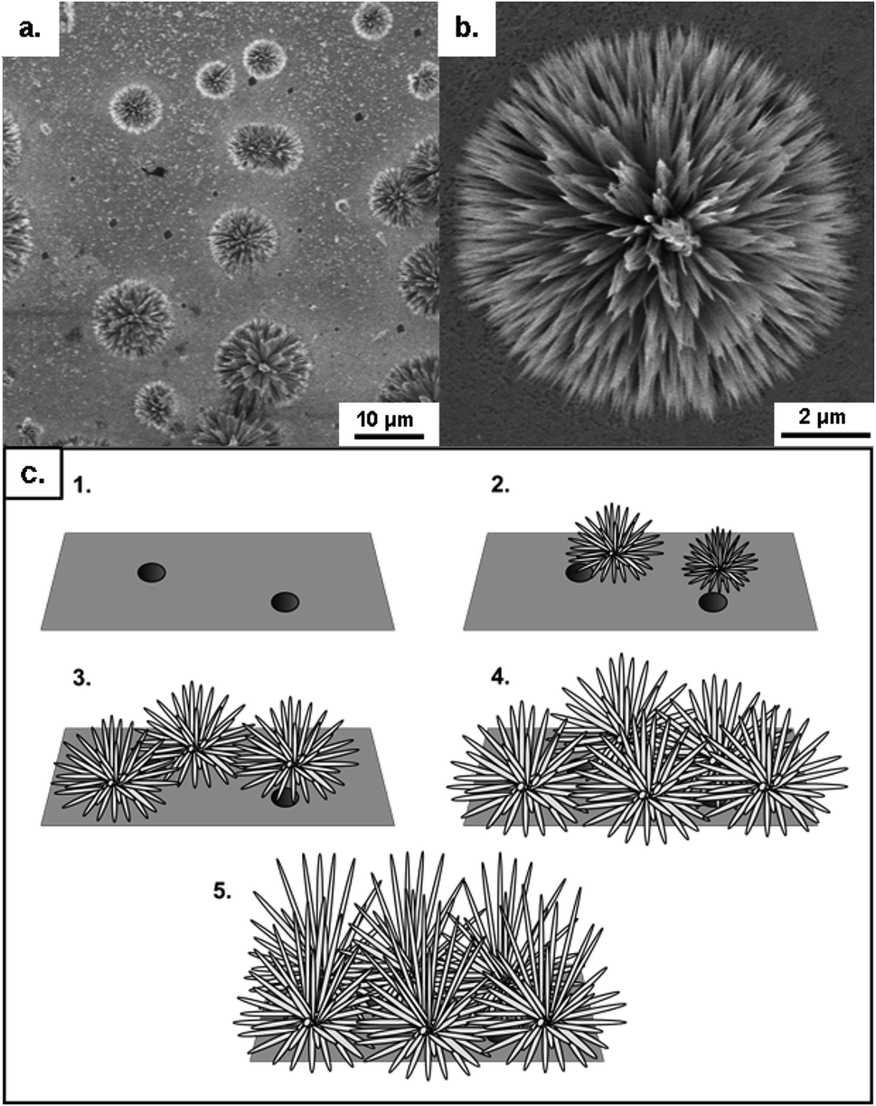 | ||
| Fig. 1 FESEM micrographs of multiple (a) and a single nanoflower (b) formed in the early growth stages and graphical representation of the initial stages of nanowire growth (c). | ||
 | ||
| Fig. 2 FESEM surface morphology (a) and cross-section (b) showing the complete coverage of the zinc surface with nanoflowers resulting in the alignment of nanowires (c). | ||
 | ||
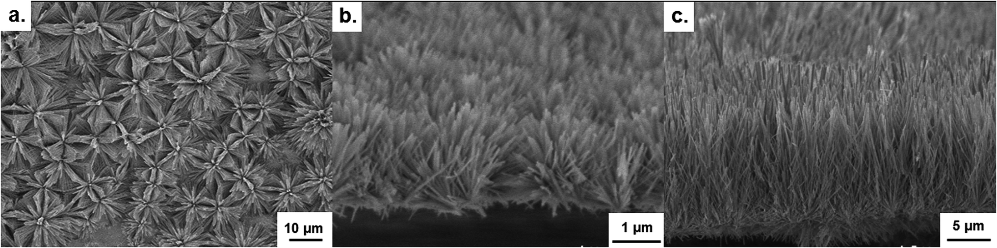
| Fig. 3 FESEM cross-sections and surface morphologies showing the initial formation of thin nanowires (a), the development of a layered structure with large hexagonal wires (b & c) and the formation of hierarchical structures (d–f). | ||
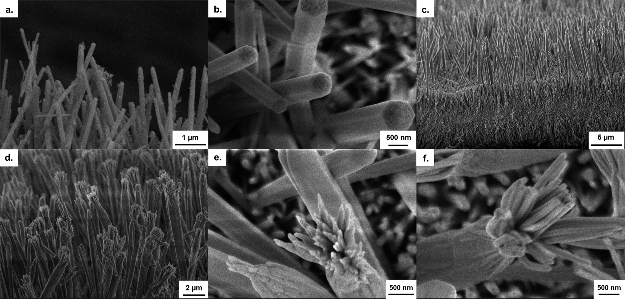
A further peculiarity in the anodization was also observed in the form of hierarchical growth. The initiation of this hierarchical growth process is shown to occur via the branching of a single large, hexagonal wire into several smaller nanowires, with diameters similar to those at the start of nanowire growth (Fig. 3d–f). These smaller nanowires, together with the underlying wires, can continue growing to form very thick nanowire films (>100 μm). At thicknesses in excess of 50 μm however, complex 3D networks of nanowires were typically formed rather than aligned nanowires.
The exact reasons for both the formation of layered films of different sized nanowires and the formation of hierarchical structures are currently unknown. This could be related to the increasing distance from the source of Zn2+ ions to the nanowire tip, thereby reducing the concentration of Zn2+ ions available for reaction. It might also be attributed to a decreasing concentration of the already dilute bicarbonate species present in the electrolyte as a function of time.
3.2 Control of nanowire growth
In the initial report on this anodization system by Hu et al., the influence of the temperature, time and voltage on the surface morphology was examined using SEM.20 These experiments highlighted some interesting features of the anodic growth, including the formation of spherical and lamellar structures at high temperatures (50–70 °C), and also cracking of films at elevated voltages (∼40 V) due to oxygen evolution beneath the nanowire films. Although these qualitative insights provided an excellent starting point in understanding this unusual growth, further quantitative measurements of the factors controlling the growth of nanostructures are necessary to be able to design bespoke hierarchical nanostructures for specific applications.In this section we examine in detail the effect of altering the conditions of voltage, temperature and time on nanowire growth and also examine the previously unstudied effects of electrolyte concentration and type. In order to gain quantitative information on growth rates under different conditions we measured the cross-sectional film thickness, corresponding to the nanowire length, via FESEM.
Although previous investigations in this area have reported the formation of nanowires in an aqueous KHCO3 electrolyte, we in fact found that this growth was also possible when either sodium or ammonium bicarbonate electrolytes were used. In both cases the nanowire growth rates were found to be significantly higher than those previously reported for anodizations in a potassium bicarbonate electrolyte.20,24 The major steps of growth presented in the previous section were found to be independent of the bicarbonate species used with only slight variations in growth rates. Therefore, in this section we present only the results from the two novel anodizations in the sodium and ammonium bicarbonate electrolytes.
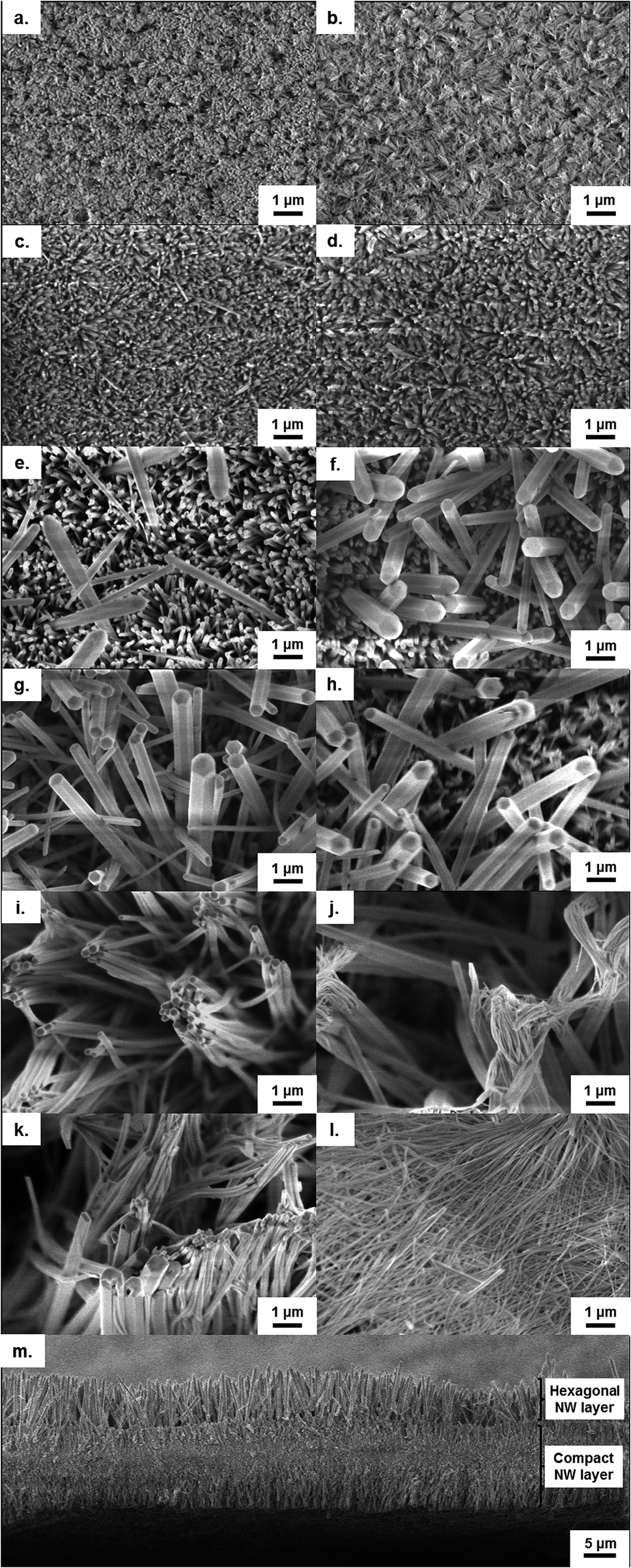 | ||
| Fig. 4 FESEM surface morphologies of nanowire (NW) films formed after anodizations for 1 (a & b), 5 (c & d), 15 (e & f), 30 (g & h), 60 (i & j) and 120 minutes (k & l) in aqueous NaHCO3 and NH4HCO3 electrolytes respectively. Representative FESEM cross-section (m) corresponding to NW film shown in (f). | ||
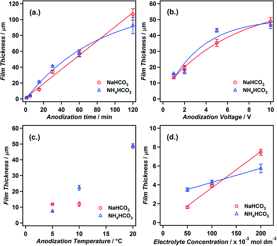 | ||
| Fig. 5 Nanowire film thicknesses obtained from FESEM for anodizations undertaken for different times (a) and at different voltages (b), temperatures (c) and electrolyte concentrations (d). Conditions used were 15 min, 5 V, 10 °C and 50 mM electrolyte concentration for (a–c) and 2 V, 10 °C and 5 minutes for (d). | ||
As homogeneous nanowire films are typically desired for applications, it is therefore important for researchers applying this technique to both select suitable voltages (2–5 V) as well as carefully control the electrochemical cell setup in order to gain reproducible results.
3.3 Rationalising the rapid nanowire growth
To make sense of the unusually rapid nanowire growth observed for such mild conditions, it was first important to try and establish the chemical structure of the nanowires in order to hypothesise possible formation mechanisms. The original study by Hu et al. postulated that the material formed from anodization in KHCO3 could be of the form Zn(CO3)n(OH)m, due to the main anions present in the solution being OH− and CO32−.20 Subsequent studies on anodization carried out under similar conditions have described the nanowires prior to annealing as being composed of either Zn(OH)2 or ZnO but with little evidence to support this.26,27Powder X-ray diffraction (pXRD) patterns of the nanowire films prior to annealing display a complex set of sharp peaks, indicating a highly crystalline material (Fig. 6). This is consistent with the observation of smooth hexagonal nanowires via FESEM. The peaks were not found to match with either ZnO, Zn(OH)2 or ZnCO3 and neither were they found to match with known hydroxy carbonates of zinc, Zn5(CO3)2(OH)6 and Zn4CO3(OH)6·H2O. Given the complex nature of the pattern, it is possible that a mixture of these materials could be present.
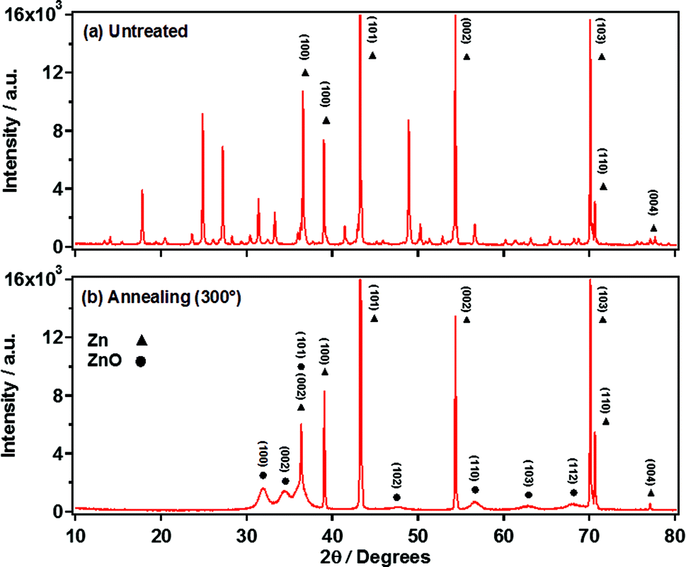 | ||
| Fig. 6 Flat plate powder XRD patterns for nanowire films obtained directly from anodization (a) and after annealing at 300 °C for 1 h (b). | ||
The X-ray photoelectron spectrum of the as-prepared nanowire film reveals a significant quantity of carbon present in addition to the expected zinc and oxygen (Fig. 7). A small quantity of iron could also be detected, which is likely to originate from the stainless steel counter electrode in the anodization setup. Analysis of the C1s region of the X-ray photoelectron spectrum reveals two peaks: a peak at lower energy attributed to adventitious carbon contamination, and a peak at slightly higher energy within the region often attributed to a metal carbonate. The latter peak is slightly shifted to higher energy compared to a typical metal carbonate which is consistent with a hydrocarbonate species.28 Since no peaks attributable to Na 1s are present it can be assumed that the hydrocarbonate peak is not due to remaining NaHCO3 from the electrolyte.
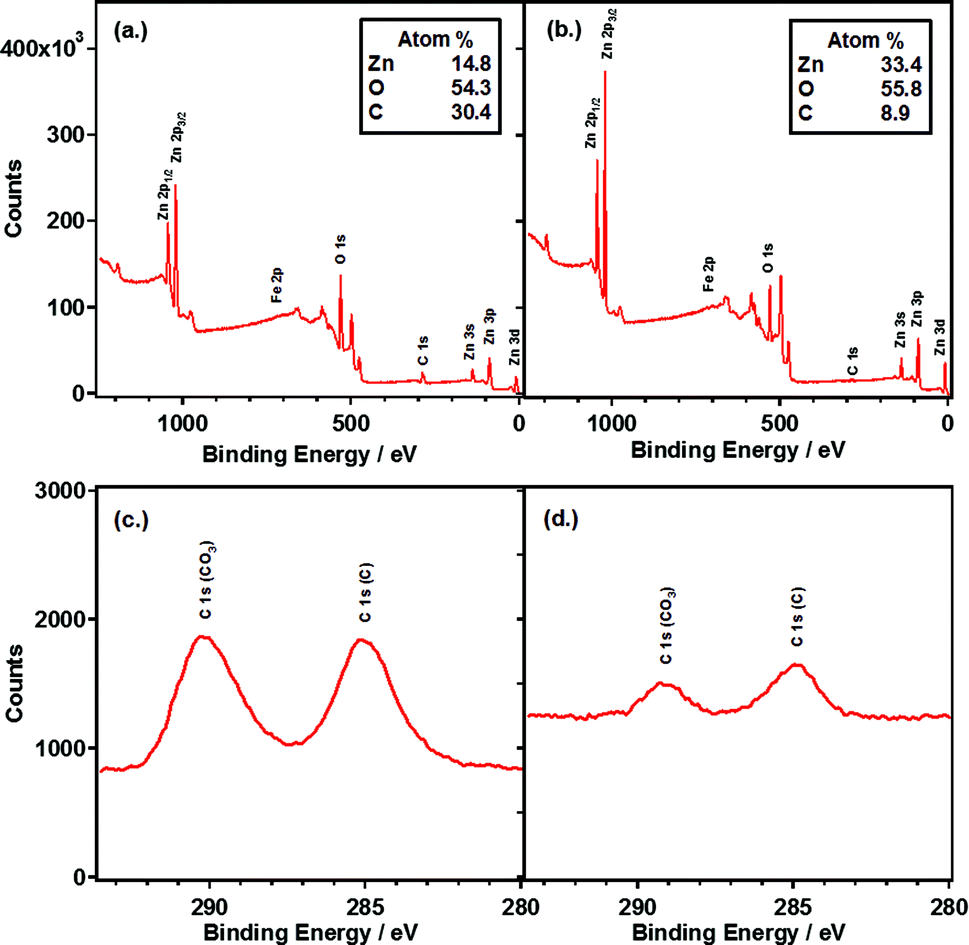 | ||
| Fig. 7 XPS survey spectra and C1s region spectra for nanowire films obtained directly from anodization (a & c) and after annealing at 300 °C (b & d). | ||
The FT-IR spectrum of the as-prepared material (Fig. S8†) also indicates the presence of carbonate and hydroxide ions, strengthening the hypothesis that the nanowires consist of a form of zinc hydroxy carbonate.
The aqueous chemistry of the zinc cation can be relatively complex with dependence on many factors including the pH, temperature, concentration and presence of other anions. The route to zinc hydroxy carbonate formation in aqueous solutions has been previously discussed by Orel et al. on the basis of a partial charge model.29,30 In water, zinc can form the relatively stable hydrated ions [Zn(OH2)6]2+ and [Zn(OH)(OH2)5]+, which can condense to form [Zn(OH)2(OH2)4] via olation and oxolation mechanisms. In the presence of HCO3−, either through dissolved CO2, or in our case through the bicarbonate electrolyte, substitution of up to two water molecules can occur to give [Zn(OH)(HCO3)(OH2)3]. Fast condensation of this species via the olation mechanism will then yield a zinc hydroxy carbonate. Based on this, we believe that the anodization could proceed via the following reactions:
| Zn(s) + 6H2O → [Zn(OH2)6]2+ + 2e− | (1) |
| [Zn(OH2)6]2+ ↔ [Zn(OH)(OH2)5]+ + H+ | (2) |
| [Zn(OH)(OH2)5]+ + HCO3− ↔ [Zn(OH)(HCO3)(OH2)3] + 2H2O | (3) |
| [Zn(OH)(OH2)5]+ ↔ [Zn(OH)2(OH2)4] + H+ | (4) |
| x[Zn(OH)2(OH2)4] + y[Zn(OH)(HCO3)(OH2)3] → [Znx+y(OH)2x(CO3)y] + 4(x + y)H2O | (5) |
| 2H+ + 2e− → H2(g) | (6) |
3.4 Conversion to ZnO and further modifications
Annealing of the nanowire films was found to yield polycrystalline ZnO. This can be observed through the broad peaks in the X-ray diffraction patterns corresponding to the wurzite form of ZnO (Fig. 6b). Although the overall nanowire form was preserved during annealing, the nanowires' facets were no longer smooth, but instead formed of multiple small nanoparticles with a “slit-pore” structure along the length of the nanowires (Fig. 8b and c). Particle sizes were determined to be 9 ± 2 nm as determined by TEM, and were found to be dependent on the annealing temperature (Fig. S9†). This interesting polycrystalline “slit-pore” structure contributes significantly towards a high specific surface area of 54.4 m2 g−1, similar to values for much smaller (<25 nm) nanoparticle powders. This high surface area, combined with the one-dimensional structure, makes these materials interesting candidates for applications such as dye-sensitized solar cells.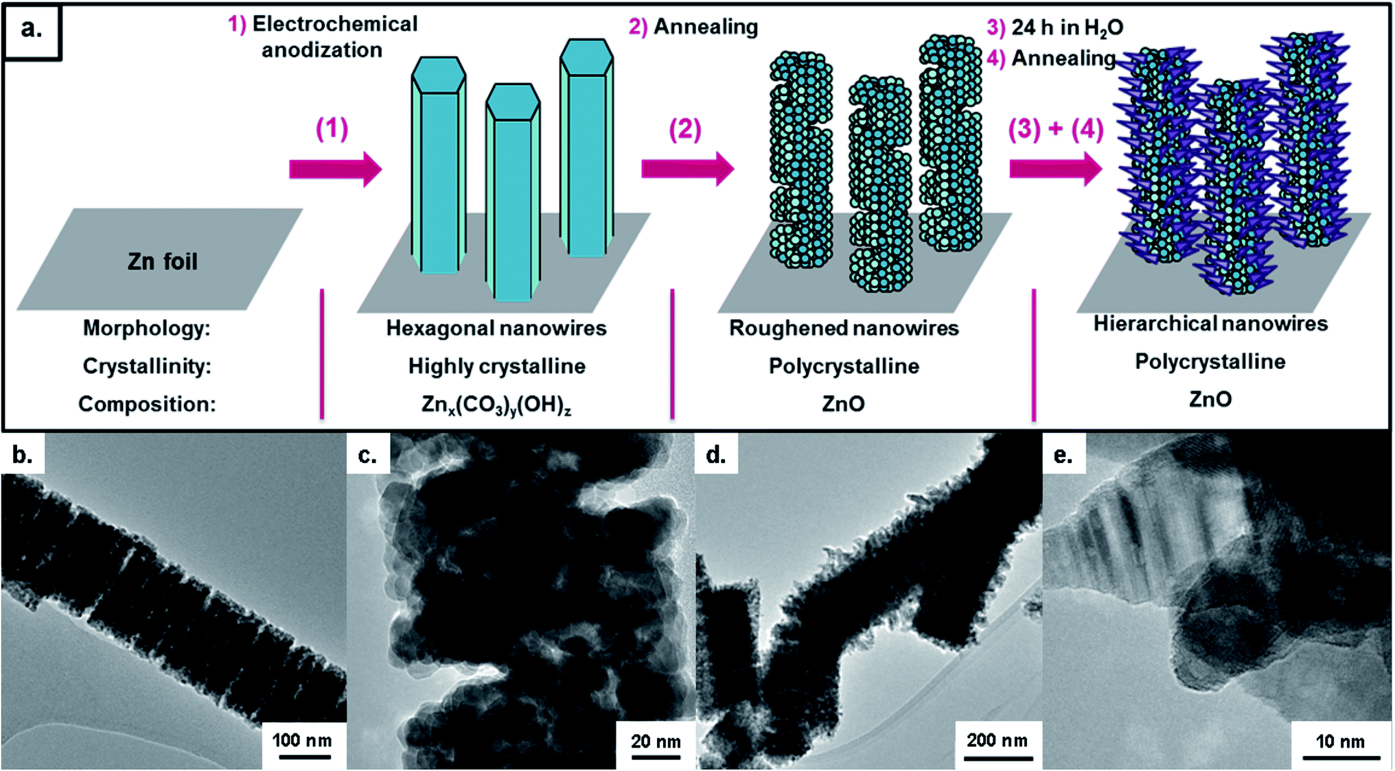 | ||
| Fig. 8 Scheme showing the two step production of polycrystalline ZnO nanowires with a “slit-pore” structure and further modification to hierarchical structures (a). TEM micrographs of the “slit-pore” nanowires (b & c) and hierarchical structures (d) with a magnified micrograph of the ZnO horns (e). | ||
An insight into the formation of this porous structure can be gained by considering the structural transformation occurring during annealing. Using the assumption that the as-prepared nanowires are a form of zinc hydroxy carbonate then degradation to ZnO will proceed via the loss of H2O and CO2.32 Using the case of hydrozincite (Zn5(CO3)2(OH)6) as an analogy, the decomposition reaction proceeds as:
| Zn5(CO3)2(OH)6 → 5ZnO + 3H2O + 2CO2 | (7) |
Loss of these two gases during heating results in a contraction between the plains of the remaining Zn and O atoms to form ZnO. As there is a higher number density of Zn atoms in the ZnO than the hydrozincite, void formation is inevitable. A decomposition such as this can explain the formation of a porous polycrystalline structure as presented here. This contraction can also be used to explain an often unwanted side-effect of the annealing process, which is cracking of the nanowire films. Cracking of the films during annealing was observed to some extent for all of the anodized films produced, even when low heating and cooling rates were used (Fig. S10†). This apparently unavoidable feature should be considered, particularly when the application requires a continuous, crack free film.
In addition to the “slit-pore” type structures, it was found that through a simple post-treatment interesting hierarchical structures could be obtained (Fig. 8d and e). This treatment involved leaving the nanowire film within a sealed vial of deionised water for 24 h, followed by another annealing treatment. The hierarchical structures consisted of horn shaped ZnO crystals of ∼40 nm in length surrounding the existing nanowire structure. These structures are likely to be the result of a slow secondary growth of ZnO onto the nanowires with hydrated zinc ions from the substrate as the ion source. The flat plate XRD pattern and XPS spectrum of the hierarchical nanowires indicate that no substance other than ZnO are present after this treatment (Fig. S11 and S12†). This simple modification may provide a route to even higher surface area nanostructures than the nanowires with slit-type pores and would therefore also be promising candidates for application in areas such as dye-sensitized solar cells and photocatalysis.
4. Conclusions
We have been able to demonstrate for the first time that the growth of high aspect ratio nanowires via the anodization of zinc can be achieved using a range of different bicarbonate electrolytes. We have also been able to show quantitatively that the reaction parameters of temperature, voltage, time and electrolyte concentration can significantly alter the nanowire growth rate. By optimising these parameters, remarkably high growth rates in excess of 3 μm min−1 can be achieved at room temperature, without destruction of the nanowire films. Examination of the properties of the nanowire films before and after annealing have allowed us to propose an explanation, both for the high growth rates achieved, and for the unique porous structure of the annealed ZnO nanowires. Furthermore, we have been able to present a simple post-treatment of the nanowires which gives rise to interesting hierarchical structures.The insights presented provide an important contribution towards the area of zinc anodization, an area that is currently ill-understood. Knowledge of the factors controlling the process, and the mechanisms underpinning them, will aid researchers in the field to design controlled hierarchical nanostructures in areas where it is likely to show promise, such as photovoltaics, photocatalysis and sensing.
Acknowledgements
The authors would like to acknowledge the Leeds EPSRC Nanoscience and Nanotechnology Research Equipment Facility (LENNF) for use of the TEM and XPS equipment. D. Miles would like to thank the EPSRC for funding through the Centre for Sustainable Chemical technologies (Grant no. EP/G03768X/1). D. Mattia would like to acknowledge the Royal Academy of Engineering for funding. All data created during this research are openly available from the University of Bath data archive at http://dx.doi.org/10.15125/BATH-00078.Notes and references
- A. Wei, L. H. Pan and W. Huang, Mater. Sci. Eng., B, 2011, 176, 1409–1421 CrossRef CAS.
- M. D. Hernandez-Alonso, F. Fresno, S. Suarez and J. M. Coronado, Energy Environ. Sci., 2009, 2, 1231–1257 CAS.
- Q. F. Zhang, C. S. Dandeneau, X. Y. Zhou and G. Z. Cao, Adv. Mater., 2009, 21, 4087–4108 CrossRef CAS.
- B. Kumar and S.-W. Kim, Nano Energy, 2012, 1, 342–355 CrossRef CAS.
- D. C. Look, D. C. Reynolds, J. R. Sizelove, R. L. Jones, C. W. Litton, G. Cantwell and W. C. Harsch, Solid State Commun., 1998, 105, 399–401 CrossRef CAS.
- C. Klingshirn, J. Fallert, H. Zhou, J. Sartor, C. Thiele, F. Maier-Flaig, D. Schneider and H. Kalt, Phys. Status Solidi B, 2010, 247, 1424–1447 CrossRef CAS.
- E. Galoppini, J. Rochford, H. Chen, G. Saraf, Y. Lu, A. Hagfeldt and G. Boschloo, J. Phys. Chem. B, 2006, 110, 16159–16161 CrossRef CAS PubMed.
- K. Subannajui, F. Guder, J. Danhof, A. Menzel, Y. Yang, L. Kirste, C. Y. Wang, V. Cimalla, U. Schwarz and M. Zacharias, Nanotechnology, 2012, 23, 235607–235613 CrossRef PubMed.
- L. E. Greene, M. Law, J. Goldberger, F. Kim, J. C. Johnson, Y. F. Zhang, R. J. Saykally and P. D. Yang, Angew. Chem., Int. Ed, 2003, 42, 3031–3034 CrossRef CAS PubMed.
- S. E. Ahn, J. S. Lee, H. Kim, S. Kim, B. H. Kang, K. H. Kim and G. T. Kim, Appl. Phys. Lett., 2004, 84, 5022–5024 CrossRef CAS.
- H. Zeng, J. Cui, B. Cao, U. Gibson, Y. Bando and D. Golberg, Sci. Adv. Mater., 2010, 2, 336–358 CrossRef CAS.
- M. Skompska and K. Zarebska, Electrochim. Acta, 2014, 127, 467–488 CrossRef CAS.
- A. M. M. Jani, D. Losic and N. H. Voelcker, Prog. Mater. Sci., 2013, 58, 636–704 CrossRef.
- G. E. J. Poinern, N. Ali and D. Fawcett, Materials, 2011, 4, 487–526 CrossRef.
- G. K. Mor, O. K. Varghese, M. Paulose, K. Shankar and C. A. Grimes, Sol. Energy Mater. Sol. Cells, 2006, 90, 2011–2075 CrossRef CAS.
- H. Tsuchiya, J. M. Macak, I. Sieber and P. Schmuki, Small, 2005, 1, 722–725 CrossRef CAS PubMed.
- I. Sieber, H. Hildebrand, A. Friedrich and P. Schmuki, Electrochem. Commun., 2005, 7, 97–100 CrossRef CAS.
- H. Tsuchiya and P. Schmuki, Electrochem. Commun., 2005, 7, 49–52 CrossRef CAS.
- S. J. Kim and J. Choi, Electrochem. Commun., 2008, 10, 175–179 CrossRef CAS.
- Z. Hu, Q. Chen, Z. Li, Y. Yu and L.-M. Peng, J. Phys. Chem. C, 2010, 114, 881–889 CAS.
- S. He, M. Zheng, L. Yao, X. Yuan, M. Li, L. Ma and W. Shen, Appl. Surf. Sci., 2010, 256, 2557–2562 CrossRef CAS.
- J. L. Zhao, X. X. Wang, J. J. Liu, Y. C. Meng, X. W. Xu and C. C. Tang, Mater. Chem. Phys., 2011, 126, 555–559 CrossRef CAS.
- A. Ramirez-Canon, D. O. Miles, P. J. Cameron and D. Mattia, RSC Adv., 2013, 3, 25323–25330 RSC.
- Y.-T. Kim, J. Park, S. Kim, D. W. Park and J. Choi, Electrochim. Acta, 2012, 78, 417–421 CrossRef CAS.
- N. Samir, D. S. Eissa and N. K. Allam, Mater. Lett., 2014, 137, 45–48 CrossRef CAS.
- S.-T. Ren, Q. Wang, F. Zhao and S.-L. Qu, Chin. Phys. B, 2012, 21, 038104–038110 CrossRef.
- J. Park, K. Kim and J. Choi, Curr. Appl. Phys., 2013, 13, 1370–1375 CrossRef.
- A. V. Shchukarev and D. V. Korolkov, Cent. Eur. J. Chem., 2004, 2, 347–362 CAS.
- M. Bitenc, P. Podbrscek, P. Dubcek, S. Bernstorff, G. Drazic, B. Orel, S. Pejovnik and Z. C. Orel, Chem.–Eur. J., 2010, 16, 11481–11488 CrossRef CAS PubMed.
- M. Bitenc, P. Podbrscek, P. Dubcek, S. Bernstorff, G. Drazic, B. Orel and Z. C. Orel, CrystEngComm, 2012, 14, 3080–3088 RSC.
- J. Livage, M. Henry and C. Sanchez, Prog. Solid State Chem., 1988, 18, 259–341 CrossRef CAS.
- X. Wang, W. Cai, Y. Lin, G. Wang and C. Liang, J. Mater. Chem., 2010, 20, 8582–8590 RSC.
Footnote |
| † Electronic supplementary information (ESI) available: FESEM surface morphologies and cross-sections for nanowire films grown at different times, temperatures, voltages and electrolyte concentrations are provided. Additional structural characterisation including FT-IR and particle size analysis. FESEM surface morphologies of nanowire film damage resulting from either high voltages or the annealing process. Typical current–time data from anodization. See DOI: 10.1039/c5ta03578c |
| This journal is © The Royal Society of Chemistry 2015 |