
 Open Access Article
 This Open Access Article is licensed under a
 Creative Commons Attribution 3.0 Unported Licence
Tin perovskite/fullerene planar layer photovoltaics: improving the efficiency and stability of lead-free devices†
Kenneth P.
Marshall
,
Richard I.
Walton
and
Ross A.
Hatton
*
Department of Chemistry, University of Warwick, Coventry, CV4 7AL, UK. E-mail: ross.hatton@warwick.ac.uk
First published on 29th April 2015
Abstract
We report the first demonstration of orthorhombic CsSnI3 films prepared from solution at room temperature that have defect densities low enough for use as the light harvesting semiconductor in photovoltaic devices even without using excess Sn in the preparative method, and demonstrate their utility in a model p–i–n photovoltaic device based on a CuI | CsSnI3 | fullerene planar layer architecture. We also report an effective strategy for simultaneously improving both the efficiency and stability of these devices towards air exposure based on the use of excess of SnI2 during CsSnI3 synthesis from CsI and SnI2. A combination of photoelectron spectroscopy, contact potential measurements and device based studies are used to elucidate the basis for this improvement and role of the excess SnI2. The open-circuit voltage in these lead-free photovoltaic devices is shown to be strongly dependent on the degree of alignment between the perovskite conduction band edge and the lowest occupied molecular orbital (LUMO) in the fullerene electron transport layer. Furthermore, the energetics at the perovskite–fullerene interface are shown to be a function both of the LUMO energy of the fullerene and the nature of the interaction at the heterojunction which can give rise to a large abrupt vacuum level shift across the interface. A champion open-circuit voltage of ∼0.55 V is achieved using indene-C60 bis-adduct as the electron extraction layer, which is twice that previously reported for a CsSnI3 based PPV.
Introduction
Over the past 4 years there has been dramatic progress in the field of perovskite photovoltaics (PPVs), most of which has focused on using methylammonium (MA) lead iodide (MAPbI3)1–4 and chloride substituted analogues, MAPbI3−xClx,5–7 as the light harvesting semiconductor. This is due to the high absorption coefficient, high charge carrier diffusion length (LD > 100 nm)8 and low band gap (Eg) of 1.5–1.6 eV![[thin space (1/6-em)]](https://www.rsc.org/images/entities/char_2009.gif) 5,9 in these materials. The highest power conversion efficiency (η) achieved to date in this field is over 19%.10
5,9 in these materials. The highest power conversion efficiency (η) achieved to date in this field is over 19%.10
The majority of PPV devices reported to date use the perovskite in a distributed heterojunction device architecture, in which n-type mesoporous TiO2 serves as the electron-transport layer (ETL) and a p-type organic semiconductor is used as the hole-transport layer (HTL). There are also a smaller number of reports of planar-heterojunction PPVs based on a p–i–n structure, including those in which TiO2 is replaced with organic semiconductors such as fullerenes, which have achieved η > 17%.11–13 Unlike TiO2, fullerene ETLs do not require annealing which removes the need for the substrate electrode to be able to withstand high temperatures. Planar device architectures using organic charge transport layers may also offer the best prospects for accommodating the very large thermal expansion exhibited by some metal halide perovskites.14 There is also interest in identifying low cost organic and inorganic HTLs, most recently the Cu(I) compounds CuI and CuSCN.15–18
The primary drawback of Pb perovskites for photovoltaic applications is their susceptibility to degradation in the presence of water to produce PbI2,19–21 which is a partially water soluble compound.21,22 Soluble Pb compounds are well known to be toxic to both humans and the natural environment23 and so there is growing interest in the development of alternative, narrow Eg perovskites that use Sn instead of Pb,24 such as CsSnI325–28 and MASnI3.29,30
At room temperature and in the absence of air CsSnI3 adopts a 3D orthorhombic perovskite structure which is known as the black phase. The Eg of this semiconductor is near optimal for PV applications (∼1.3 eV14),31 which combined with its high optical absorption coefficient (∼104 cm−1 in the visible region)32 and low exciton binding energy (∼18 meV),33 makes CsSnI3 attractive as a light harvesting semiconductor in PPVs because photoexcitation results in free carrier generation for light with wavelengths as long as ∼950 nm.14 However, the material is prone to the formation of a high density of Sn cation vacancy defects, which serve as p-type dopants and recombination centres.14,34
Sn perovskites also have the drawback of air sensitivity, with the black phase converting to yellow phase CsSnI3, which in turn oxidises to Cs2SnI6 in which Sn is in its more stable 4+ oxidation state.14,35 Unlike Sn, Pb is most stable in the 2+ oxidation state due to the relativistic lowering of the Bohr radius of s-orbitals more than that of other atomic orbitals, which stabilises them towards oxidation, an effect that is most pronounced in heavy p-block elements like Pb.36,37 In practice the ingress of oxygen and moisture into PV devices is inevitable and so a central challenge in Sn-PPV research is to develop strategies that can be used in conjunction with device encapsulation to reduce the rate of oxidation of Sn perovskite enough for practical applications to be possible. To date there have been six literature reports relating to the use of Sn perovskites in PPVs which collectively demonstrate the potential to achieve high η.25–30
CsSnI3 was first used by Chung et al.25 as a HTL in PPVs in which a ruthenium dye was the primary light harvesting element and the CsSnI3 was synthesised using a vacuum melt process at 450 °C. That pioneering work was quickly followed by Chen et al.,26 who demonstrated a Schottky contact type PPV based on a vacuum evaporated layer of CsSnI3 formed by sequential deposition of alternating layers of CsI and SnCl2 followed by annealing at 175 °C to form the perovskite, although the device fill factor (FF) was extremely low (∼0.22) due to a very low shunt resistance and high series resistance. Concurrently to this Zhou et al.38 reported that CsSnI3 could be synthesised at room temperature from a mixed solution of CsI and SnI2, although films formed using that method were not tested for optoelectronic applications. In 2014 Noel et al. reported the highest η to date for a Sn PPV of ∼6%, achieved using MASnI3 as the light harvesting semiconductor.29 However those devices were also shown to exhibit a very large variation in performance and poor stability with deeply coloured devices becoming completely transparent minutes after measuring.29 That work was published only days before a report by Hao et al.30 who showed that η close to 6% could be achieved using MASnIBr2 and the open-circuit voltage (Voc) could be tuned by varying the ratio of iodide to bromide as a result of a change in Eg. Shortly afterwards Kumar et al.27 reported that CsSnI3 processed at 70 °C and with 20 mol% SnF2 additive could be used as the light absorber in a PPV device based on a distributed heterojunction with TiO2, achieving photocurrents >22 mA cm−2. Unfortunately the Voc and fill factor (FF) were limited to ∼240 mV and ∼0.37 respectively which constrained η to 2.02%. Notably, devices fabricated without SnF2 did not function and whilst it was shown that fluoride was not incorporated into the CsSnI3 lattice, the possible optoelectronic functionality of the relatively large quantity of SnF2 present in the perovskite film was not discussed.27 Kumar et al. concluded that the Voc in CsSnI3 PVs is limited by the high background carrier density due to Sn-vacancy defects even when prepared under Sn-rich conditions, and is not set by the difference between the conduction band minimum of the ETL and the valence band maximum (or highest occupied molecular orbital (HOMO)) of the HTL. The same group went on to show that substitution of iodide by bromide in CsSnI3 is an effective means of increasing the Voc in Sn-PPV achieving a Voc of 0.41 V. However, the improvement in Voc was at the expense of photocurrent due to the increase in Eg.28
Herein we report: (i) the first demonstration of orthorhombic CsSnI3 films prepared from solution at room temperature with defect densities low enough for use as the light harvesting semiconductor in PPV devices, even in the absence of excess Sn; (ii) a new strategy for improving device stability towards oxidation in air, which does not complicate the process of device fabrication; (iii) the results of a study which unambiguously show that the energetics at the interface between CsSnI3 and ETL are a key determinant of device Voc.
Results
Model p–i–n PPVs were fabricated with the structure: indium tin oxide (ITO)|CuI|CsSnI3|fullerene|bathocuproine (BCP)|Al, as schematically illustrated in Fig. 1a. The CsSnI3 layer was prepared from 8 wt% CsSnI3 in N,N-dimethylformamide (DMF) using SnI2 and CsI. CuI was chosen as the p-type material due to its proven effectiveness as a HTL in PPVs.15 CuI is also amenable to deposition by both thermal evaporation and by solution processing. Since thermal evaporation enables a very high degree of control over film thickness and morphology it is the preferred method in this study. Likewise C60 was selected as the n-type material because it can also be deposited by thermal evaporation. There are also a number of simple derivatives of C60 commercially available with modified frontier orbital energies. For these reasons C60 serves as a model n-type charge extraction layer in this work. The CsSnI3 layer was deposited by spin casting directly onto freshly evaporated CuI at room temperature to give films with a thickness of ∼50 nm, as measured using cross-sectional AFM histogram analysis (Fig. 1b(ii)). In contrast to all other reports relating to the use of Sn-perovskites in PPVs these films were used without post-deposition annealing. | ||
| Fig. 1 (a) Schematic of the device architecture used in this work; (b(i)) SEM image of a CsSnI3 film prepared with a 10 mol% excess SnI2 and spin cast at 4000 rpm from 8 wt% solution onto an ITO glass substrate coated with a 100 nm layer of CuI; (b(ii)) AFM step height of a scored CsSnI3 film spin cast from 8 wt% solution onto glass; (c) SEM image of a CsSnI3 film spun from 15 wt% CsSnI3 solution with 10 mol% SnI2 excess using the same deposition process and substrate as for (b(i)). | ||
Fig. 1b(i) shows a representative SEM image of a CsSnI3 film deposited from 8 wt% CsSnI3 in DMF onto a CuI coated ITO substrate. The film is made up of small crystals approximately 50–100 nm in diameter, which is comparable to the film thickness determined from a step edge analysis using atomic force microscopy (Fig. 1b(ii) and (ESI) Fig. S1a–c†). It is therefore likely that these crystallites extend from the top to the bottom of the film as schematically depicted in Fig. 1a. Increasing the loading of CsSnI3 to 15 wt% resulted in an increase in film thickness to ∼80 nm with a larger mean crystallite size and very few pin holes (Fig. 1c and ESI Fig. S1d–f†). Whilst there are still some gaps in films of this thickness the coverage is exceptionally high for such a thin layer of metal halide perovskite.11 Furthermore, films of comparable quality could also be prepared on glass, ITO and Au coated substrates which proved useful for fundamental measurements of film properties.
A representative X-ray diffraction (XRD) pattern of a CsSnI3 film spin cast onto a glass substrate pre-coated with 10 nm of evaporated CuI is shown in Fig. 2b. The very thin CuI layer is included to ensure the structure of the perovskite film probed is identical to that used in PPV devices. Since there is no evidence of CuI in the XRD pattern it can be concluded that the buried CuI layer is essentially amorphous and/or too thin to be observed using this technique. The XRD pattern in Fig. 2b is consistent with the orthorhombic perovskite structure expected for the black phase of CsSnI3, as reported in the literature14 and simulated in Fig. 2a. The prominence of the peaks at ∼29° in the XRD pattern of the film as compared to the simulated powder pattern is indicative of preferential crystal orientation in the spin cast film on CuI. The small reflections at ∼26.3°,∼27.7° and ∼37.8° (starred) are associated with the supporting substrate and sample holder. After 16 hours air exposure the CsSnI3 film gives the XRD pattern Fig. 2e, which is consistent with the formation of the Cs2SnI6, in which Sn is in the more stable 4+ oxidation state, as is evident from the good agreement with the simulated reflections for Cs2SnI6 shown in Fig. 2d.39 X-ray photoelectron spectroscopy (XPS) measurements of the oxygen 1s binding energy shows that those Sn atoms that do not form part of Cs2SnI6 structure are most likely present as SnO2 (ESI Fig. S2†). The absence of reflections in the XRD pattern indicative of crystalline SnO2 indicates that it is present as an amorphous or nano-crystalline phase.
 | ||
| Fig. 2 X-ray diffraction (XRD) patterns of films of: (a) a simulated powder diffraction pattern of CsSnI3; (b) a thin film of CsSnI3; (c) a thin film of CsSnI3 prepared with a 10 mol% excess SnI2; (d) a simulated powder diffraction pattern of Cs2SnI6, and (e) a CsSnI3 film oxidised in air for 16 hours. All films probed using XRD were supported on glass substrates coated with 10 nm CuI and deposited by spin casting at 2000 rpm from 16 mol% DMF solutions. | ||
It has recently been proposed that due to the ease with which Sn-cation vacancies form in CsSnI3 it must be prepared in a Sn-rich environment or at high temperature to ensure the density of these defects is low enough for its use as a light harvesting material in PPV devices.27,34,35 However we find that devices based on CsSnI3 films prepared using stoichiometric mixtures of CsI and SnI2 with no excess of Sn and processed entirely at room temperature generate a short circuit current density (Jsc) of ∼10 mA cm−2 under 1 sun simulated solar illumination, which is a very high current for such a thin semiconductor layer (∼50 nm) (Fig. 3). The incident-photon-to-converted-electron (IPCE) efficiency (ESI Fig. 3†) confirms that CsSnI3 is the primary light absorbing component in these devices, since wavelengths as long as ∼930 nm are converted into electrons in the external circuit, which corresponds to sub-band gap photon energies for C60. This spectral response is also consistent with Eg for CsSnI3 reported in the literature of ∼1.3 eV.14,35
 | ||
| Fig. 3 Scatter graphs of PPV performance characteristics for devices with the structure: ITO|CuI|CsSnI3|C60|BCP|Al using CsSnI3 prepared from solutions containing either 0, 5 or 10 mol% excess SnI2. The mean values are shown as red squares. | ||
As shown in Fig. 3, devices based on CsSnI3 films prepared using an excess of SnI2 and C60 ETL exhibit up to ∼30% increase in Jsc and Voc as compared to those without. The optimal SnI2 excess is ∼10 mol% which results in a doubling of η from ∼0.75% to ∼1.5%. All reflections in the XRD pattern for films prepared using 10 mol% excess SnI2 (Fig. 2c) can be attributed to CsSnI3, except the weak reflection at ∼28.5°. The latter cannot be assigned to SnI2 or its oxidised form; SnI4, which indicates that the excess SnI2 is nano-crystalline or amorphous. High-resolution XPS measurements of the surface chemical composition of freshly prepared films with a 10 mol% SnI2 excess show that there is very little SnI2 and no evidence for SnI4 at the CsSnI3 surface (Fig. S4†), since ∼95% of the photoelectrons originate from the top ∼7 nm of the sample. The XPS data therefore provides evidence that the 10 mol% excess SnI2 phase separates to the buried interface upon solvent evaporation. Notably, since these films were unavoidably exposed to the laboratory for ∼1 minute when transferring from the nitrogen filled glove box to the spectrometer vacuum system there is also evidence for significant oxidation of the surface of the CsSnI3 to Cs2SnI6 in the XPS spectra.
If the excess SnI2 is primarily located at the buried CsSnI3|CuI interface it must be capable of transporting holes from CsSnI3 into CuI since PPV devices incorporating up to 15 mol% SnI2 perform comparably to those with 5% SnI2 excess (Fig. 3). To our knowledge there are no previous reports of SnI2 being used as a semiconductor in an organic or hybrid electronic device and so its charge transport properties are not known. To investigate the transport properties of SnI2 we have estimated the hole-mobility in SnI2 from the space charge limited current in unipolar diodes to be 2.2–5.1 × 10⁻⁶ cm2 V−1 s−1 (ESI, Fig. S5†). Whilst this value is low as compared to that of Sn and Pb halide perovskites it is comparable to that of many amorphous organic semiconductors40 and offers an explanation as to why device FF begins to deteriorate with increasing SnI2 excess beyond 10 mol%. To determine the accessibility of the SnI2 valence band for hole transport we have measured the ionisation potential (Ip) of SnI2 (Ip ∼ 5.64 eV ± 0.05 eV) and CuI films (Ip ∼ 5.84 eV ± 0.05 eV) using ultraviolet photo-electron spectroscopy (UPS). Full details of the UPS study are given in the (ESI Fig. S6 and S7†). These energy levels, along with the Eg for CuI determined from electronic absorption measurements (ESI, Fig. S8†) and Eg for SnI2 taken from the literature,41 are given in Fig. 4a. The susceptibility of CsSnI3 films to oxidation in air prevented us from making a reliable measurement of the CsSnI3Ip using UPS, and the values reported in the literature for argon sputtered CsSnI3 – also measured using UPS – vary from 4.9 eV25 to 5.7 eV.41 In order to estimate the position of the valence and conduction band edges in CsSnI3 with confidence we have measured the work function of CsSnI3 films without air exposure, or argon sputtering, using a Kelvin probe located in the same glove box as the spin coater used to deposit the perovskite film. On the basis of this measurement, combined with the known Eg (∼ 1.3 eV) and knowledge of the tendency of this material to form p-type defects,27,34,35 we have estimated the possible range of energies for the valence and conduction band edges in CsSnI3. These energy levels along with the work function of each material measured using the Kelvin probe technique are given in Fig. 4a. It is clear from the location of the Fermi level in CuI that it is heavy p-doped which is consistent with literature reports43 and can be attributed to Cu atom array vacancies. In the absence of such intrinsic defects CuI would block the extraction of holes from the CsSnI3 valance band due to its very deep lying valance band. However, the high density of electron acceptor states near to the valence band edge should ensure that there is no barrier to hole-extraction from CsSnI3 when thermodynamic equilibrium is established across the interface. Similarly, spontaneous electron transfer from the SnI2 into CuI due to the difference in Fermi level would be expected to remove the relatively small barrier to hole-extraction from SnI2 into CuI. On the basis of the energy levels given in Fig. 4a there would however be expected to be a significant barrier to hole-transport from the CsSnI3 valence band into the SnI2 valence band. However, since the current–voltage characteristics of PPV devices fabricated with an excess of SnI2 in the CsSnI3 layer (up to 15 mol%) are not consistent with a high device series resistance it is likely that there is a favourable vacuum level shift at the interface due to the formation of an interfacial dipole.
 | ||
| Fig. 4 (a) Schematic energy level diagram depicting the valence band edge for CuI and SnI2 films measured using UPS. The conduction band edge for CuI has been estimated from the electronic absorption spectrum (ESI, S8†). The energy of the conduction band edge for SnI2 is estimated based on the reported Eg for SnI2.44 The work function of freshly UV/O3 treated ITO glass, CuI, SnI2 and CsSnI3 measured using the Kelvin probe technique are also shown; (b) the evolution of εvacf at the surface of a freshly deposited CsSnI3 film with increasing thicknesses of thermally evaporated C60 measured using the Kelvin probe technique. The error bars represent maximum and minimum values. | ||
The improvement in Jsc and Voc in PPV devices using a CsSnI3 layer prepared with excess SnI2 can be rationalised in terms of a reduction in the background carrier density which gives rise to recombination loses, since it is known that the density of Sn-vacancy defects (i.e. the primary source of the background carrier density) is suppressed when the perovskite is synthesised in a Sn-rich environment.27,34,35 However, to investigate the possibility that the energetics at the perovskite|C60 interface might also plays a role in controlling Voc we have measured the change in energy between the perovskite Fermi level and the surface vacuum level (vac) as a function of the C60 layer thickness using the Kelvin probe method. This energy difference, εvacf, corresponds to the work function of C60 when the film thickness is sufficient for the establishment of Fermi level alignment across the interface. If thermodynamic equilibrium is not achieved then εvacf corresponds to the work function of the perovskite with a modified surface potential.42,43 Changes in εvacf can therefore be interpreted in terms of a vacuum level shift which give rises to a comparable shift in the energy of the HOMO and LUMO in the C60 with respect the valance and conduction band edges in CsSnI3. The results of this experiment are summarised in Fig. 4b. At the interface between CsSnI3 prepared with 0% excess SnI2 there is no significant change in the energy of the vacuum level. Conversely for films prepared with 10 mol% excess SnI2 there is a large abrupt positive vacuum level shift of ∼0.3 eV meV. Abrupt positive vacuum level shifts at the interface between inorganic materials and organic semiconductors are relatively rare42,43 and are indicative of ground state charge transfer from the substrate into the first layer of molecule forming an interfacial dipole. The reason for the stronger interaction between C60 and CsSnI3 with fewer Sn-vacancy sites is not yet clear, although the existence of this abrupt positive vacuum level shift offers an alternative explanation for the increase in Voc, since it would operate to reduce the loss in electron potential energy when moving from the perovskite conduction band into the fullerene LUMO.
To further investigate the extent to which Voc in these devices is controlled by the degree of alignment between the LUMO of the ETL and the conduction band edge in CsSnI3, we have systematically reduced the LUMO energy of the ETL from ∼4.00 eV45,46 to ∼3.91 eV46 and finally to ∼3.74 eV46 below the vacuum level by substituting C60 with the C60 derivatives [6,6]-phenyl-C61-butyric acid methyl ester (PC60BM) and indene-C60 bis-adduct (IC60BA) (Fig. 4a). Whilst the exact magnitude of these values remain the subject of debate45 the differences in LUMO energy between these derivatives is firmly established.45,46 Champion J/V characteristics in the dark and under 1 sun simulated illumination are given in Fig. 5 and the full data set is given in the ESI (Table S1†). It is clear from Fig. 5 and the full data set in (Table S1†) that the increase in device Voc correlates with an increase in the LUMO energy of the fullerene ETL which is consistent with a reduction in the potential energy lost by an electron moving from the CsSnI3 into the ETL as seen in organic PVs.46 The highest η is achieved for devices using ICBA as the ETL at 2.76%, which is significantly higher than the best previously reported for a CsSnI3 based PPV (2.02%).27 Collectively these data show that the performance of PPVs based on CsSnI3 depends strongly on the energetics at the interface between the CsSnI3 and the ETL, much like that seen at donor/acceptor heterojunctions in OPVs.46
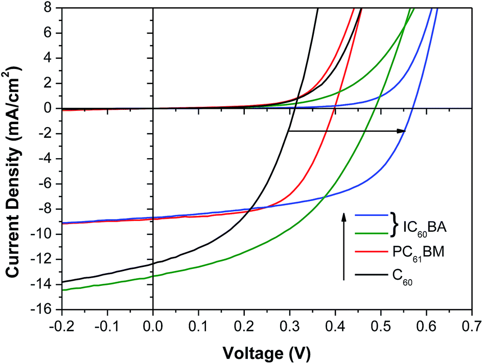 | ||
| Fig. 5 Dark and light JV curves of best performing PPV devices with the structure ITO|CuI|CsSnI3 + 10 mol% SnI2|fullerene|BCP|Al, using different fullerene ETLs. For the case of ICBA the device Voc was found to be strongly dependent on the concentration of the ICBA solution used: 3 mg ml−1 ICBA (green), 5 mg ml−1 ICBA (blue), although was always higher than that achieved in devices using PCBM when all other parts of the device were identical. | ||
For practical applications the stability of the light harvesting semiconductor towards oxidation in air is critically important. Encouragingly PV devices based on CsSnI3 prepared in a Sn-rich environment have been reported to be stable for more than 250 hours when stored in glove box,27 although – to our knowledge – the stability of Sn perovskite PVs in air has not be quantitatively reported. We find that the use of excess SnI2 in the preparation of CsSnI3 dramatically improves device stability. Fig. 6 shows the key performance parameters of unencapsulated PPV devices (using C60 as the ETL) as a function of SnI2 excess in the CsSnI3 layer. The data points in the hashed region correspond to device performance immediately after fabrication and after storage for 10 days in a nitrogen filled glove box (<5 ppm O2 and <0.1 ppm H2O). For devices based on CsSnI3 films prepared using stoichiometric amounts of CsI and SnI2 the η of is reduced by ∼70% after this ten day period of storage due to the combined effect of deteriorated Jsc, Voc and FF. Conversely devices based on CsSnI3 with 10 mol% excess SnI2 exhibit a relatively small reduction in η of ∼10% due primarily to a reduction in FF. These devices were then bought into the laboratory and the performance tested as a function of time. Devices with 0 mol% excess SnI2 stopped working altogether after ∼30 minutes air exposure due to a complete collapse in Jsc. Conversely devices with 10 mol% excess SnI2 exhibit dramatically improved stability such that even after 14 hours in air without encapsulation they still function, albeit with a Jsc of one fifth the starting value. Both the FF and Voc are essentially stable during this period.
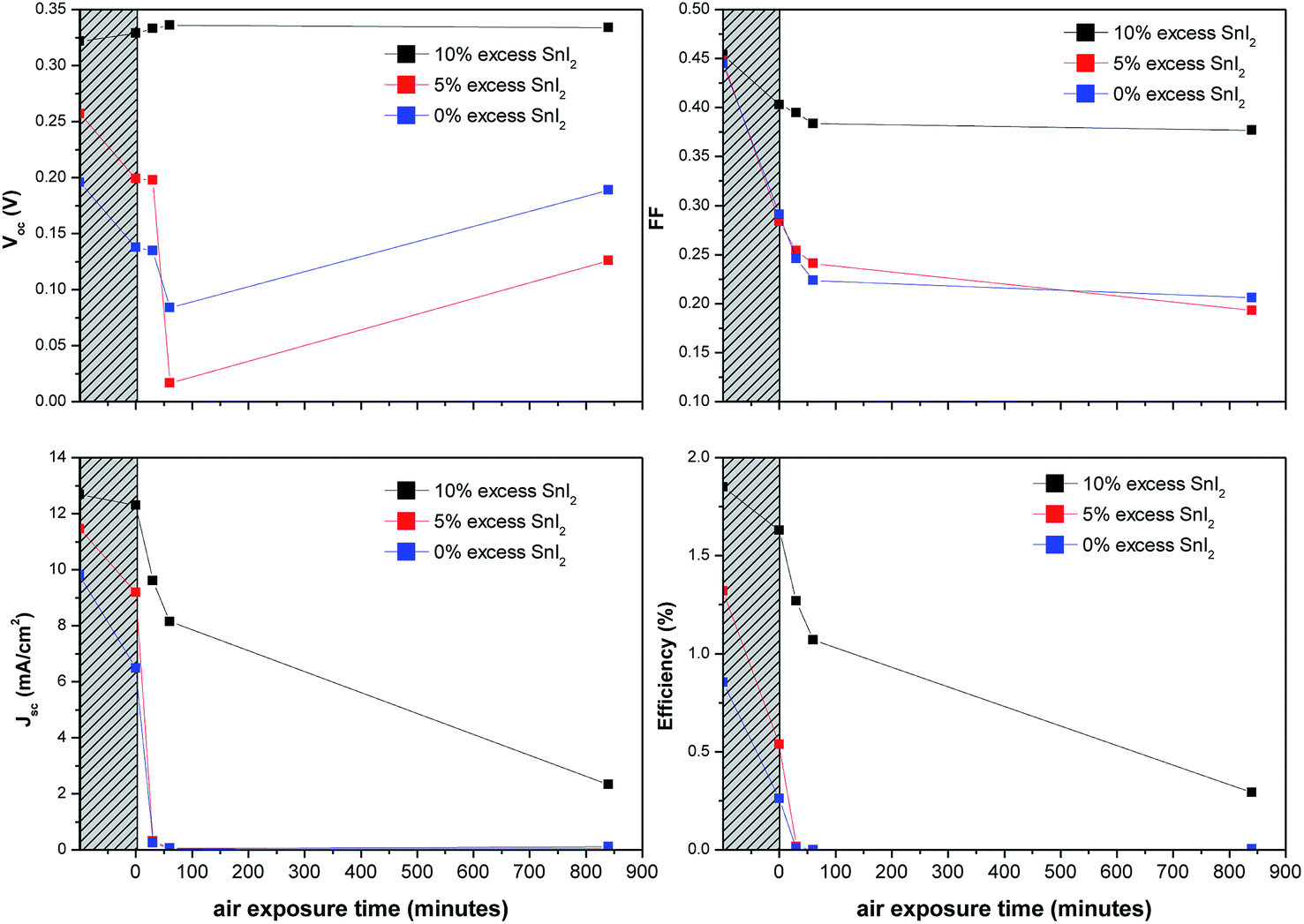 | ||
| Fig. 6 Key device performance characteristics for unencapsulated PPV devices with the structure ITO|CuI|CsSnI3|C60|BCP|Al using CsSnI3 prepared from solutions containing either 0, 5 or 10 mol% excess SnI2. The data in the hashed region correspond to device performance immediately after fabrication and then again after storage in a nitrogen atmosphere (<5 ppm O2 and <0.1 ppm H2O) for 10 days. These devices were then bought into laboratory and the performance was measured as a function of time stored in air. | ||
It is likely that the deterioration in device performance upon exposure to the laboratory environment results from a number of parallel degradation mechanisms some of which are not related to the perovskite layer, such as oxidation of the Al cathode and/or doping of the C60 layer by oxygen.47 However, since it is evident from our XPS studies (ESI, Fig. S4†) that oxidation of CsSnI3 in air to form Cs2SnI6 is a very rapid process and that Cs2SnI6 in known to absorb light very weakly as compared to CsSnI3,41 it is likely that conversion of CsSnI3 into Cs2SnI6 is major contributor to the continuous deterioration in Jsc. This conclusion is supported by the evolution of the absorption spectra of CsSnI3 films on glass, with and without 10 mol% SnI2, as a function of time exposed to air ((ESI, Fig. 9†)), from which it is evident that the addition of 10 mol% SnI2 greatly reduces the rate of oxidation of the CsSnI3. Since this process would be expected to begin at the interface with the ETL any significant change in the energetics at this interface for electron extraction as a result of this transformation would manifest as a change in device series resistance and FF, the effect of which would be most pronounced in the early stages of oxidation process when the potential energy step forms. Cs2SnI6 has been shown to have a relatively high electron and hole mobility48 although its conduction band edge is ∼200 meV deeper lying than that of CsSnI341 and so the formation of a Cs2SnI6 layer between the remaining CsSnI3 and C60 would most likely impede the flow of electrons from the conduction band of the CsSnI3 into the LUMO of the C60 resulting in an increase in device series resistance and reduction in FF, as is observed to be the case. To test the generality of this result for another fullerene ETL and to remove the complexity associated with possible doping of the fullerene layer by oxygen upon exposure to air we have fabricated PPV devices using PCBM as the ETL with and without exposure of the CsSnI3 layer to air for 1 minute, before transferring back into the glove box to complete device fabrication. Typical J–V characteristics for PPV devices with and without exposure of the perovskite layer to air are given in Fig. 7 from which it is clear that devices incorporating an excess of SnI2 are much more stable than those without and that the changes in Jsc, Voc and FF after 1 minute air exposure are consistent with that in Fig. 6.
 | ||
| Fig. 7 Representative J–V characteristics of PPV devices with the structure: ITO|CuI 70 nm|CsSnI3 (with and without 10 mol% excess SnI2) |PCBM|BCP|Al: (a) CsSnI3 with no excess SnI2; (b) CsSnI3 with 10 mol% excess SnI2. Graphs show devices made entirely in glove box (black) and those made using a CsSnI3 layer exposed to the laboratory environment for 1 minute (red) before being returned to the glove box to complete fabrication and testing. | ||
Finally, we have tested the stability of devices, with and without 10 mol% excess SnI2 in the CsSnI3 layer, over a period of four hours continuous illumination in a nitrogen atmosphere. Representative results are given in Fig. 8, from which it is clear that devices incorporating excess SnI2 exhibit greatly improved stability including a stable Voc and FF after the first 20 minutes. Whilst Jsc deteriorates rapidly by ∼10% within the first 50 minutes the rate of reduction in Jsc then slows markedly. Conversely devices with no excess of CsSnI3 exhibit a continuous rapid decline in FF and Jsc.
 | ||
| Fig. 8 Graphs showing the effect of constant illumination (100 mW cm−2 of AM 1.5) for 245 minutes. Device structure; ITO|CuI (70 nm)| CsSnI3 + 0% or 10% SnI2 (8 wt%, 4000 rpm)|PC61BM (15 mg ml−1, 1000 rpm)|BCP (8 nm)|Al (50 nm). | ||
Collectively the aforementioned stability studies show that the use of a 10 mol% excess of SnI2 in CsSnI3 preparation imparts dramatically improved device stability, which indicates that the stability of CsSnI3 towards oxidation is very sensitive to the density of Sn vacancy defects. Since the transformation of CsSnI3 into Cs2CsI6 requires the loss of Sn it seems plausible that at the site of a Sn vacancy in CsSnI3 the barrier to transformation into Cs2SnI6 is reduced. It is also possible that the excess SnI2 occupies some of the space between adjacent CsSnI3 crystallites thereby impeding the ingress of the oxygen and water that gives rise to oxidation.
Conclusion
In summary we have demonstrated the preparation of orthorhombic CsSnI3 films from solution at room temperature with defect densities low enough for use as the light harvesting semiconductor in photovoltaic devices, even without the addition of excess Sn. We have shown how the Voc in a model planar layer device based on a CuI|CsSnI3|fullerene p–i–n structure can be doubled from ∼0.28 V to ∼0.55 V by engineering the energetics at the CsSnI3/fullerene interface. To our knowledge, the champion device Voc, FF and η are the highest that have been reported using CsSnI3 as the light harvesting semiconductor in a PPV by a considerable margin. We have also demonstrated a simple and effective strategy for improving the stability of PPV devices based on CsSnI3 and have rationalised the reason for this improvement using a combination of photoelectron spectroscopy, contact potential measurements and device based studies. This work shows that if tin-halide perovskites are prepared in a tin rich environment, in order to minimise the density of Sn vacancy defects, then consideration must be made as to the charge transport properties of the source of the excess tin.Materials
CuI (Sigma-Aldrich, 99.999%), CsI (Sigma-Aldrich 99.9%), SnI2 (Alfa Aesar, 99.999%), PC61BM (Nano-C, 99.5%), indene-C60 bis-adduct (IC60BA) (Ossila, 99.5%), C60 (Nano-C, 99.5%), bathocuproine (Alfa Aesar, 98%), N,N-dimethylformamide (DMF) (VWR, anhydrous, 99.8%), chlorobenzene (Sigma-Aldrich, anhydrous, 99.8%), acetone (Sigma-Aldrich, GPR, ≥99%), propan-2-ol (Sigma-Aldrich, HPLC, 99.8%), deionised H2O (pureit dispenser, >10 MΩ). CsI and non-anhydrous solvents were stored in air. All other chemicals were stored in nitrogen filled glove box (<5 ppm O2 and <0.1 ppm H2O).Synthesis of caesium tin(II) iodide
CsI was added to SnI2 in a 1:1.1 molar ratio under nitrogen. To this DMF was added to make an 8 wt% solution which is bright yellow in colour. The solution was shaken for a few minutes until all CsI and SnI2 had dissolved and was left overnight before use. The perovskite material precipitated on spin casting to give dark red/brown coloured films.
Device fabrication
Solar cells were fabricated on indium tin oxide (ITO) coated glass slides (Thin Film Devices Inc., 15 ± 3 Ω sq−1). The slides were prepared by cleaning the ITO using acetone, water and isopropanol in an ultrasound bath for 10 minutes each followed by UV/O3 treatment for 15 minutes. The slides were then loaded into a dry nitrogen filled glove box for device fabrication. 70–100 nm thick CuI films were deposited onto the ITO glass substrates by thermal evaporation. CuI can also be deposited by spin casting a 50 mg ml−1 in chlorobenzene:di-n-propyl sulfide (5.5:1) at 1000 rpm. Onto this 8 wt% CsSnI3 with a 10 mol% excess of SnI2 was spin cast at 4000 rpm from a DMF solution for 60 s. 40 nm of C60 was the deposited by thermal evaporation at a rate of 0.1–0.4 nm s−1. PC61BM was spin cast at 1000 rpm from 15 mg ml−1 chlorobenzene solution, and IC60BA from 3, 5 or 7 mg ml−1 chlorobenzene solutions for 60 s. The PCBM and ICBA solutions were filtered with a 0.2 μm PTFE syringe filter before use. Finally 8 nm of bathocuproine (BCP) followed by 50 nm of Al were deposited by thermal evaporation at a rate of 0.5–1 Å s−1. The Al was evaporated through a mask to produce 0.06 cm2 pixels. For devices without CuI, ITO was cleaned in the same way, but was put under the UV/O3 lamp for 5 minutes longer to help the perovskite film wet the surface.
Device testing
Device testing was performed in the same glove box as used for device fabrication unless otherwise stated. Current–voltage (J–V) curves were measured using a Keithley 2400 source-meter under AM1.5G solar illumination at 100 mW cm−2 (1 sun) by sweeping from −1 V to +1 V in 0.01 V increments at a rate of 0.1 V s−1. There was no significant current–voltage hysteresis, as shown in Fig. S10.† IPCE measurements were carried out using a Sciencetech SF150 xenon arc lamp and a PTI monochromator, with the monochromatic light intensity calibrated using a Si photodiode (Newport 818-UV). The incoming monochromatic light was chopped at 500 Hz. For signal measurement a Stanford Research Systems SR 830 lock-in amplifier was used.X-ray diffraction
CsSnI3 films were spin cast from 16 wt% DMF solutions at 2000 rpm onto glass slides coated with 10 nm of CuI. The X-ray diffraction patterns were collected under a flow of nitrogen using a Cu Kα1/2 source in θ–θ mode on a Bruker D8 Advance powder diffractometer equipped with an Anton-Paar HTK900 gas chamber. Patterns were corrected for the height of the sample by calibrating the 2θ axis against reference patterns. Simulated diffraction patterns were calculated using the program Mercury 3.1 with CIFs from the Inorganic Crystal Structure Database (ICSD).UPS and XPS
UPS and XPS were performed on freshly prepared CsSnI3 films spin cast onto Au substrates. The samples were exposed to the laboratory environment for ∼1 min prior to loading into the ultra-high vacuum system. UPS spectra were recorded using UV photons with energy 21.22 eV from a He I plasma source. The X-ray photoelectron spectroscopy (XPS) measurements were carried out in a UHV system with a base pressure of 5 × 10⁻¹¹ mbar. The sample was excited with X-rays from a mono-chromated Al Kα source (hν = 1486.6 eV) with the photoelectrons being detected at a 45° take-off angle using an Omicron Sphera electron analyser.Acknowledgements
This work was supported by the UK Engineering and Physical Science Research Council and European Regional Development Agency/Advantage West Midlands Science City Materials Initiative (Project 2). We thank Dr Marc Walker (University of Warwick, Department of Physics) for assistance with the XPS and UPS data collection.Notes and references
- A. Kojima, K. Teshima, Y. Shirai and T. Miyasaka, J. Am. Chem. Soc., 2009, 131, 6050–6051 CrossRef CAS PubMed.
- J. M. Ball, M. M. Lee, A. Hey and H. J. Snaith, Energy Environ. Sci., 2013, 6, 1739–1743 CAS.
- B. Cai, Y. Xing, Z. Yang, W.-H. Zhang and J. Qiu, Energy Environ. Sci., 2013, 6, 1480–1485 CAS.
- L. Etgar, P. Gao, Z. Xue, Q. Peng, A. K. Chandiran, B. Liu, M. K. Nazeeruddin and M. Grätzel, J. Am. Chem. Soc., 2012, 134, 17396–17399 CrossRef CAS PubMed.
- S. Colella, E. Mosconi, P. Fedeli, A. Listorti, F. Gazza, F. Orlandi, P. Ferro, T. Besagni, A. Rizzo, G. Calestani, G. Gigli, F. De Angelis and R. Mosca, Chem. Mater., 2013, 25, 4613–4618 CrossRef CAS.
- M. M. Lee, J. Teuscher, T. Miyasaka, T. N. Murakami and H. J. Snaith, Science, 2012, 338, 643–647 CrossRef CAS PubMed.
- M. Liu, M. B. Johnston and H. J. Snaith, Nature, 2013, 501, 395–398 CrossRef CAS PubMed.
- S. D. Stranks, G. E. Eperon, G. Grancini, C. Menelaou, M. J. P. Alcocer, T. Leijtens, L. M. Herz, A. Petrozza and H. J. Snaith, Science, 2013, 342, 341–344 CrossRef CAS PubMed.
- H.-S. Kim, C.-R. Lee, J.-H. Im, K.-B. Lee, T. Moehl, A. Marchioro, S.-J. Moon, R. Humphry-Baker, J.-H. Yum, J. E. Moser, M. Grätzel and N.-G. Park, Sci. Rep., 2012, 2, 591 Search PubMed.
- H. Zhou, Q. Chen, G. Li, S. Luo, T.-B. Song, H.-S. Duan, Z. Hong, J. You, Y. Liu and Y. Yang, Science, 2014, 345, 542–546 CrossRef CAS PubMed.
- J.-Y. Jeng, Y.-F. Chiang, M.-H. Lee, S.-R. Peng, T.-F. Guo, P. Chen and T.-C. Wen, Adv. Mater., 2013, 25, 3727–3732 CrossRef CAS PubMed.
- C. Zuo and L. Ding, Nanoscale, 2014, 6, 9935–9938 RSC.
- W. Nie, H. Tsai, R. Asadpour, A. J. Neukirch, G. Gupta, J. J. Crochet, M. Chhowalla, S. Tretiak, M. A. Alam and H. Wang, Science, 2015, 347, 522–525 CrossRef CAS PubMed.
- I. Chung, J.-H. Song, J. Im, J. Androulakis, C. D. Malliakas, H. Li, A. J. Freeman, J. T. Kenney and M. G. Kanatzidis, J. Am. Chem. Soc., 2012, 134, 8579–8587 CrossRef CAS PubMed.
- J. A. Christians, R. C. M. Fung and P. V. Kamat, J. Am. Chem. Soc., 2014, 136, 758–764 CrossRef CAS PubMed.
- N. J. Jeon, J. Lee, J. H. Noh, M. K. Nazeeruddin, M. Grätzel and S. Il Seok, J. Am. Chem. Soc., 2013, 135, 19087–19090 CrossRef CAS PubMed.
- J. Wang, S. Wang, X. Li, L. Zhu, Q. Meng, Y. Xiao and D. Li, Chem. Commun., 2014, 50, 5829–5832 RSC.
- A. S. Subbiah, A. Halder, S. Ghosh, N. Mahuli, G. Hodes and S. K. Sarkar, J. Phys. Chem. Lett., 2014, 5, 1748–1753 CrossRef CAS.
- G. Niu, W. Li, F. Meng, L. Wang, H. Dong and Y. Qiu, J. Mater. Chem. A, 2014, 2, 705 CAS.
- M. A. Green, A. Ho-Baillie and H. J. Snaith, Nat. Photonics, 2014, 8, 506–514 CrossRef CAS.
- M. Grätzel, Nat. Mater., 2014, 13, 838–842 CrossRef PubMed.
- H. L. Clever and F. J. Johnston, J. Phys. Chem. Ref. Data, 1980, 9, 751–784 CrossRef CAS PubMed.
- F. Bischoff, L. C. Maxwell, R. D. Evans and F. R. Nuzum, J. Pharmacol. Exp. Ther., 1928, 34, 85–109 CAS.
- Y. Ogomi, A. Morita, S. Tsukamoto, T. Saitho, N. Fujikawa, Q. Shen, T. Toyoda, K. Yoshino, S. S. Pandey and S. Hayase, J. Phys. Chem. Lett., 2014, 5, 1004–1011 CrossRef CAS.
- I. Chung, B. Lee, J. He, R. P. H. Chang and M. G. Kanatzidis, Nature, 2012, 485, 486–489 CrossRef CAS PubMed.
- Z. Chen, J. J. Wang, Y. Ren, C. Yu and K. Shum, Appl. Phys. Lett., 2012, 101, 093901 CrossRef PubMed.
- M. H. Kumar, S. Dharani, W. L. Leong, P. P. Boix, R. R. Prabhakar, T. Baikie, C. Shi, H. Ding, R. Ramesh, M. Asta, M. Graetzel, S. G. Mhaisalkar and N. Mathews, Adv. Mater., 2014, 26, 7122–7127 CrossRef CAS PubMed.
- D. Sabba, H. K. Mulmudi and R. R. Prabhakar, J. Phys. Chem. C, 2015, 119, 1763–1767 CAS.
- N. K. Noel, S. D. Stranks, A. Abate, C. Wehrenfennig, S. Guarnera, A. Haghighirad, A. Sadhanala, G. E. Eperon, S. K. Pathak, M. B. Johnston, A. Petrozza, L. Herz and H. Snaith, Energy Environ. Sci., 2014, 7, 3061–3068 CAS.
- F. Hao, C. C. Stoumpos, D. H. Cao, R. P. H. Chang and M. G. Kanatzidis, Nat. Photonics, 2014, 8, 489–494 CrossRef CAS.
- W. Shockley and H. J. Queisser, J. Appl. Phys., 1961, 32, 510–519 CrossRef CAS PubMed.
- K. Shum, Z. Chen, J. Qureshi, C. Yu, J. J. Wang, W. Pfenninger, N. Vockic, J. Midgley and J. T. Kenney, Appl. Phys. Lett., 2010, 96, 221903 CrossRef PubMed.
- Z. Chen, C. Yu, K. Shum, J. J. Wang, W. Pfenninger, N. Vockic, J. Midgley and J. T. Kenney, J. Lumin., 2012, 132, 345–349 CrossRef CAS PubMed.
- P. Xu, S. Chen, H. Xiang, X. Gong and S. Wei, Chem. Mater., 2014, 26, 6068–6072 CrossRef CAS.
- C. C. Stoumpos, C. D. Malliakas and M. G. Kanatzidis, Inorg. Chem., 2013, 52, 9019–9038 CrossRef CAS PubMed.
- U. Kaldor and S. Wilson, Theoretical Chemistry and Physics of Heavy and Superheavy Elements, 2003 Search PubMed.
- P. Pyykkö, Chem. Rev., 1988, 88, 563–594 CrossRef.
- Y. Zhou, H. F. Garces, B. S. Senturk, A. L. Ortiz and N. P. Padture, Mater. Lett., 2013, 110, 127–129 CrossRef CAS PubMed.
- W. Werker, Recl. Trav. Chim. Pays-Bas Belg., 1939, 58, 257–258 CrossRef CAS PubMed.
- T. G. Plint, B. a. Kamino and T. P. Bender, J. Phys. Chem. C, 2015, 119, 1676–1682 CAS.
- J. Zhang, C. Yu, L. Wang, Y. Li, Y. Ren and K. Shum, Sci. Rep., 2014, 4, 6954 CrossRef CAS PubMed.
- B. H. Ishii, K. Sugiyama, E. Ito and K. Seki, Adv. Mater., 1999, 11, 605–625 CrossRef.
- S. R. Day, R. A. Hatton, M. A. Chesters and M. R. Willis, Thin Solid Films, 2002, 410, 159–166 CrossRef CAS.
- P. Ravindran, A. Delin, R. Ahuja, B. Johansson, S. Auluck, J. Wills and O. Eriksson, Phys. Rev. B: Condens. Matter Mater. Phys., 1997, 56, 6851–6861 CrossRef CAS.
- B. W. Larson, J. B. Whitaker, X. Wang, A. A. Popov, G. Rumbles, N. Kopidakis, S. H. Strauss and O. V. Boltalina, J. Phys. Chem. C, 2013, 117, 14958–14964 CAS.
- Y. He, H. Y. Chen, J. Hou and Y. Li, J. Am. Chem. Soc., 2010, 132, 1377–1382 CrossRef CAS PubMed.
- N. Grossiord, J. M. Kroon, R. Andriessen and P. W. M. Blom, Org. Electron., 2012, 13, 432–456 CrossRef CAS PubMed.
- B. Lee, C. C. Stoumpos, N. Zhou, F. Hao, C. Malliakas, C. Yeh, T. J. Marks, M. G. Kanatzidis and R. P. H. Chang, J. Am. Chem. Soc., 2014, 136, 15379–15385 CrossRef CAS PubMed.
Footnote |
| † Electronic supplementary information (ESI) available: Further characterisation data. See DOI: 10.1039/c5ta02950c |
| This journal is © The Royal Society of Chemistry 2015 |