
 Open Access Article
 This Open Access Article is licensed under a
 Creative Commons Attribution 3.0 Unported Licence
Nickel oxide interlayer films from nickel formate–ethylenediamine precursor: influence of annealing on thin film properties and photovoltaic device performance†
K. X.
Steirer
*acd,
R. E.
Richards
a,
A. K.
Sigdel‡
bc,
A.
Garcia§
c,
P. F.
Ndione
c,
S.
Hammond
c,
D.
Baker¶
d,
E. L.
Ratcliff
e,
C.
Curtis
c,
T.
Furtak
d,
D. S.
Ginley
c,
D. C.
Olson
c,
N. R.
Armstrong
a and
J. J.
Berry
*c
aDepartment of Chemistry and Biochemistry, University of Arizona, Tucson, Arizona, USA
bDepartment of Physics and Astronomy, University of Denver, Denver, Colorado, USA
cNational Renewable Energy Laboratory, Golden, Colorado, USA. E-mail: Kenneth.Steirer@NREL.GOV; Joseph.Berry@NREL.GOV
dApplied Physics Department, Colorado School of Mines, Golden, Colorado, USA
eDepartment of Materials Science and Engineering, University of Arizona, Tucson, Arizona, USA
First published on 17th April 2015
Abstract
An organometallic ink based on the nickel formate–ethylenediamine (Ni(O2CH)2(en)2) complex forms high performance NiOx thin film hole transport layers (HTL) in organic photovoltaic (OPV) devices. Improved understanding of these HTLs functionality can be gained from temperature-dependent decomposition/oxidation chemistries during film formation and corresponding chemical structure-function relationships for energetics, charge selectivity, and transport in photovoltaic platforms. Investigations of as-cast films annealed in air (at 150 °C–350 °C), with and without subsequent O2-plasma treatment, were performed using thermogravimetric analysis, Fourier transform infrared spectroscopy, ultraviolet and X-ray photoelectron spectroscopy, and spectroscopic ellipsometry to elucidate the decomposition and oxidation of the complex to NiOx. Regardless of the anneal temperature, after exposure to O2-plasma, these HTLs exhibit work functions greater than the ionization potential of a prototype donor polymer poly(N-9′-heptadecanyl-2,7-carbazole-alt-5,5-(4′,7′-di-2-thienyl-2′,1′,3′-benzothiadiazole) (PCDTBT), thereby meeting a primary requirement of energy level alignment. Thus, bulk-heterojunction (BHJ), OPV solar cells made on this series of NiOx HTLs all exhibit similar open circuit voltages (Voc). In contrast, the short circuit currents increase significantly from 1.7 to 11.2 mA cm−2 upon increasing the anneal temperature from 150 °C to 250 °C. Concomitantly, increased conductivity and electrical homogeneity of NiOx thin films are observed at the nanoscale using conductive tip-AFM. Similar Voc observed for all the O2-plasma treated NiOx interlayers and variations to nanoscale conductivity suggest that the HTLs all form charge selective contacts and that their carrier extraction efficiency is determined by the amount of precursor conversion to NiOx. The separation of these two properties: selectivity and conductivity, sheds further light on charge selective interlayer functionality.
Introduction
High efficiency bulk heterojunction (BHJ) organic photovoltaic (OPV) devices often require contacts modified with hole or electron charge-transport interlayers in order to increase the charge carrier collection efficiency above that of the unmodified transparent conducting oxide or metal contact.1,2 The efficiency of charge collection interlayers relies upon their thin film conductivity,3 work function (Φw),4–7 alignments of interlayer valence and conduction band edges with the highest occupied molecular orbital (HOMO) and lowest unoccupied molecular orbital (LUMO) energies across the heterojunction,8–12 as well as the degree of heterogeneity for the contact surface.13 The combination of these mechanisms provide for selective charge collection in competition with bimolecular and surface recombination under low internal electric fields (i.e. near open-circuit conditions).14–16 In particular, the importance of selectivity and contact-extraction efficiency becomes increasingly important in solution-processed photovoltaic platforms as free carrier mobilities of photo-active layers increase. Metal oxides formed with Mo, V, W, Ni or NiCo6 have been shown to exhibit favorable attributes as hole transport layers (HTLs). Photovoltaic applications in organic-,17–22 colloidal quantum structure-23,24 and methyl ammonium lead halide-based platforms25–27 utilize HTLs with high transmission at operational wavelengths and work function (Φw) values equal to or in excess of the donor IP value, although presumably due to different mechanisms for n- and p-type oxides. The grand challenge in contact design remains to effectively create solution-processed deposition methods for high performing thin film devices while still maintaining material and interfacial functionalities outlined above.NiOx, is one of few p-type metal oxides that has transversed numerous energy relevant technologies such as catalysis, batteries, fuel cells and photovoltaics. Hence, it is of fundamental interest and several organometallic precursor formulations compatible with solution processing have been identified for thin film formation. Examples of these are: nickel acetate tetrahydrate complexed with methanolamine (275 °C);28 nickel nitrate hexahydrate with monoethanolamine (500 °C)29 and nickel formate dihydrate with ethylenediamine (250 °C).30 Lowering the processing temperature required to convert these precursors to the oxide allows use of plastic substrates, which in general cannot tolerate prolonged processing above 150 °C.31 There is considerable literature precedent for the decomposition of nickel formate to form Ni and NiO.32–38 Diamine complexation with nickel formate lowers the thermal requirement for decomposition and thus enables formation of NiOx at lower temperature. Solutions made with the complexed organometallic precursor in ethylene glycol and water allow fabrication of NiOx thin films by spin coating the nickel formate–ethylenediamine–ethylene glycol–water (Ni(O2CH)2–en–eg–water) ink followed by thermal annealing in air. Formation of NiOx by this method is unique as it produces conformal, high performance thin films with few processing steps.
A detailed understanding of the interconnected decomposition chemistry with the material and interface functionality can drive metal oxide ink development beyond empirical approaches. For example, exposure to reactive oxygen during annealing may further reduce thermal post-treatments. Zhai et al. demonstrated this relaxation in processing conditions for the acetate precursor, below 150 °C.39 As a direct result of the film growth and processing, NiOx interlayers strongly affect the OPV device performance.28,30,40 After annealing in air and treating with an O2-plasma, NiOx outperforms a benchmark HTL of poly(ethylene dioxythiophene):poly(styrene sulfonate) (PEDOT:PSS) in prototypical OPV devices using the BHJ poly[N-9′-heptadecanyl-2,7-carbazole-alt-5,5-(4′,7′-di-2-thienyl-2′,1′,3′-benzothiadiazole] (PCDTBT):[6,6]-phenyl-C71 butyric acid methyl ester (PC70BM).20 When NiOx interlayers are included in OPV devices, the surface chemistry, band edge energies and mid-gap defect states determine the surface electrical properties and charge selectivity towards holes. Detailed spectroscopic analyses of these solution-deposited NiOx thin films have shown that these are complex NiOx surfaces, with a wide range of possible oxide stoichiometries that influence their optoelectronic properties, and their interactions with semiconductors such as those found in organic and hybrid photovoltaic platforms.8,25–27,41 Previous UPS and XPS measurements on these films correlated surface hydroxyl species and their dipolar character with an increased band gap energy and improved band edge alignment with BHJ films.8,41 More specifically, the NiOx surface formed from decomposition of these solution precursors is comprised predominantly of a mixture of NiOx, Ni(OH)2 and NiOOH, as revealed by XPS characterization.41 The dipolar character of this modified surface leads to a high Φw and favorable energetic matching to the highest occupied molecular orbital (HOMOD) hole-transport energy level of PCDTBT, while the wide band gap, and an apparent lack of mid-gap states, functions to block reverse electron transfer from the lowest unoccupied molecular orbital (LUMOA) of the fullerene electron acceptor.8,20,41 Furthermore, as these processing conditions for the NiOx interlayers led to variations in the measured local density of states observed in UPS, this resulted in higher hole selectivity and lower leakage currents in hole only devices.41 Through improved charge selectivity and limiting carrier injection from the contact, these NiOx interlayers lower leakage current and increase shunt resistance in OPV devices.14,42 However, systematic investigation of precursor decomposition in relation to device performance has yet to be addressed and hence, is the focus of this paper.
Here, we study the effects of varying the annealing temperature between 150 °C and 350 °C for thin films spin coated from the Ni(O2CH)2–en–eg–water formulation. The effects of incomplete precursor decomposition are important to understanding their influence on the interlayer optoelectronic properties and the ability to collect photocurrent in OPV devices. We observe changes to both the chemical and electronic properties of the resulting NiOx thin films that correlate with large changes in short-circuit photocurrent (Jsc) and little to no changes in open-circuit photovoltage (Voc) in PCDTBT:PC70BM OPV devices. Decomposition/oxidation reactions for the films were investigated by thermal gravimetric analysis (TGA), differential scanning calorimetry (DSC), Fourier transform infrared absorption spectroscopy (FTIR) and X-ray photoelectron spectroscopy (XPS). By increasing the anneal temperature for thin films spin-coated from the Ni(O2CH)2–en–eg–water ink, from 150 °C to above 250 °C, and subjecting the films to an O2-plasma, amorphous thin films are formed with: (i) increased conductivity as measured by conductive AFM; (ii) increased surface oxygen content (O/Ni ratio revealed by XPS); (iii) increase of the NiOx band gap; (iv) high performance in OPV devices, as revealed by analysis of their series resistance and Jsc. Voc is shown to be affected primarily by the surface oxidation chemistry of NiOOH even if the precursor decomposition/oxidation is incomplete, while losses observed in Jsc depend primarily upon the nanoscale conductivity threshold reached upon decomposition of the Ni-formate–diamene complex. These studies decouple the underlying oxide formation from the surface effects by O2-plasma treating for photovoltaic device applications.
Experimental
Ink preparation
Preparation of the Ni(O2CH)2–en–eg precursor formulation for NiOx films has been reported earlier.30 To summarize, nickel formate (1 g) was combined with ethylene glycol (10 ml) followed by ethylenediamine (0.87 ml). The mixture was heated and shaken multiple times, and then filtered at near ambient temperature through a 0.45 μm pore filter. The ink was a deep purple color, consistent with the violet color reported for Ni(O2CH)2(en)2.43 For spin coating, the ink was diluted 1![[thin space (1/6-em)]](https://www.rsc.org/images/entities/char_2009.gif) :1 by volume with water (nanopure).
:1 by volume with water (nanopure).
Thin films & devices
Patterned ITO substrates were first solvent cleaned in acetone and isopropyl alcohol followed by an O2-plasma treatment. NiOx films were deposited by spin coating the Ni(O2CH)2–en–eg–water ink at 4000 rpm onto the ITO substrates and immediately annealing the films in air at 150–400 °C for one hour. After annealing, all NiOx layers were exposed to O2-plasma treatment for 2 minutes at 155 W and 800 mTorr. The 1:4 ratio PCDTBT:PC70BM solution was prepared in 1,2-dichlorobenzene under an inert atmosphere at a total concentration of 35 mg ml−1. The solution was stirred at 90 °C for 8 hours before cooling to 60 °C followed by immediate use, which is a variation on a previously reported procedure.20 Spin coated active layers were deposited on top of the NiOx HTL films at a spin rate of 2000 rpm for 120 seconds. The coated substrates were annealed at 70 °C on a hot plate for one hour. Top electrodes composed of Ca/Al (20 nm/100 nm) were thermally evaporated using an Angstrom Engineering thermal evaporator with a base pressure below 1 × 10⁻⁷ Torr to produce 0.11 cm2 devices. Films of NiOx were prepared on freshly O2-plasma cleaned Au substrates for AFM and C-AFM studies.
AFM & C-AFM
Scanning probe measurements employed an Asylum Research MFP-3D Atomic Force Microscope in conductive mode (c-AFM) using a Pt/Cr coated conductive tip (ElectricMulti75-G by Budget Sensors Inc.) with a radius less than 25 nm. Both height topography and c-AFM were obtained simultaneously. To obtain a good c-AFM signal, NiOx films were deposited on top of Au-coated glass substrates rather than ITO, since ITO has non-uniform conductive regions44 and thermally-induced electrical degradation at small length scales.13 The Au substrate used for calibration had a highly uniform c-AFM profile at very small sample-to-tip bias (VST). All c-AFM measurements on NiOx films were at ambient conditions with identical scan parameters such as scan speed and drive amplitude, using a VST of 40 mV.Photoelectron spectroscopy
Experiments were performed on a Kratos Axis Ultra X-ray photoelectron spectrometer equipped with a monochromatic Al K-alpha X-ray source (hv 1486.6 eV) and a He UV source (hv 21.22 eV). Linear calibration of the binding energy scale for the detector was performed following the procedure outlined by M. P. Seah.45 A bias of −10.00 V was applied to the sample during UPS experiments to spectrally separate the lowest kinetic energy electrons and secondary electrons from the local environment. An Ar sputter-etched, atomically-clean gold sample was measured before characterization of the NiOx samples to establish the Fermi edge of the spectrometer.TGA & DSC
The ink (nickel formate–ethylenediamine–ethylene glycol–water) was placed in a Pt pan at 120 °C to evaporate the bulk of the water and ethylene glycol solvent with minimal disruption of the nickel formate–ethylenediamine complex. This procedure was repeated twice to obtain an initial mass of 13.87 mg of the NiOx film precursor (less ethylene glycol). The pan temperature was increased at 10 °C min−1 under dry synthetic air (20% O2, 80% N2) in a TA Instruments SDT Q600 operated in TGA/DSC mode.FTIR
Transmission spectra were measured using a Thermo-Nicolet 6700 FTIR. A liquid N2-cooled mercury–cadmium-telluride (MCT) detector and a KBr beamsplitter were used. Scans were collected to provide data with a resolution of 2 cm−1. For each measurement 100 scans were averaged for both the sample and the background. Absorbance spectra were calculated from the sample and background using the Beer–Lambert equation.Ellipsometry
Thin film optical properties and thicknesses (9.5 ± 0.5 nm) were characterized using an M-2000 spectroscopic ellipsometer (J.A. Woolam Co Inc.) at wavelengths of 250–1000 nm and angle of 65–75 degrees. Spectroscopic ellipsometry data were processed with the aid of WVASE software. The NiOx complex refractive index constants (N = n − ik) were obtained using a Lorentz parameterized model, which is consistent with the Kramers–Kronig relations. Thicknesses were verified using a Dektak 8 stylus profilometer.Results and discussion
1. Decomposition and oxidation of Ni(O2CH)2(en)2
Decomposition and oxidation processes for the metal organic precursor depends on the nickel complex formed in solution and spin cast into films. We follow the conversion to NiOx with TGA and DSC shown in Fig. 1. Previous literature isothermal studies have reported the complete decomposition/oxidation of Ni(O2CH)2·2H2O (at 240 °C–280 °C in air)38 and Ni(O2CH)2 (at 215–250 °C in oxygen and 242–262 °C in air).35,36 For example, Ni(O2CH)2·2H2O was converted to NiO in less than an hour at 240 °C–280 °C in air.38 This is consistent with the expectation that the films annealed in this study at 250 °C or 300 °C in air should be comprised of NiOx, which is also supported by the decomposition/oxidation temperature for the Ni(O2CH)2(en)2 complex observed by TGA/DSC in Fig. 1. Narain reported the synthesis of Ni(O2CH)2(en)2, which should be robust at 120 °C without any loss of the ethylenediamine ligand.43 Therefore, the DSC/TGA measurements (Fig. 1) were performed in a Pt pan on an ink sample after two rounds of evaporation of the bulk of the ethylene glycol and water solvents at 120 °C, leaving a sufficient mass of primarily the Ni(O2CH)2(en)2 complex. On heating in synthetic air (80% N2, 20% O2), a small endothermic peak is evident near 125 °C, with a corresponding mass loss of ca. 5%, which is interpreted as a loss of residual solvent (water, ethylene glycol, excess ethylenediamine). Between 180–240 °C, an additional 77% of the initial mass (81% of mass at 150 °C) is lost in an endothermic process, which is comparable to the expected 72% mass change for conversion of Ni(O2CH)2(en)2 to NiO. Mass loss is due to a combination of evaporation of residual solvent (likely ethylene glycol, boiling point 197 °C), loss of the ethylenediamine ligands, which have been shown to leave stepwise,46–48 and the decomposition/oxidation of the Ni(O2CH)2 complex (above 225 °C) to NiOx.34,36,38 In comparison, studies with [Ni(saccharinate)2(en)2]en47 [Ni(en)3]oxalate,48 Ni(succinate)(en),49 and Ni(en)3SO4 (ref. 50) reported temperatures for the final stage decomposition/oxidation to NiO of 300 °C, 325 °C, 410 °C, and 466 °C respectively. On further heating, there is some additional mass lost (ca. 2% of the initial mass) until 375 °C, when an exothermic transition is seen and correlates with a gradual mass increase. Hence, the Ni(O2CH)2(en)2 complex is to date, preferred for lower temperature formation of solution-deposited NiOx but photovoltaic applications require subsequent surface treatments to increase the work-function.7,30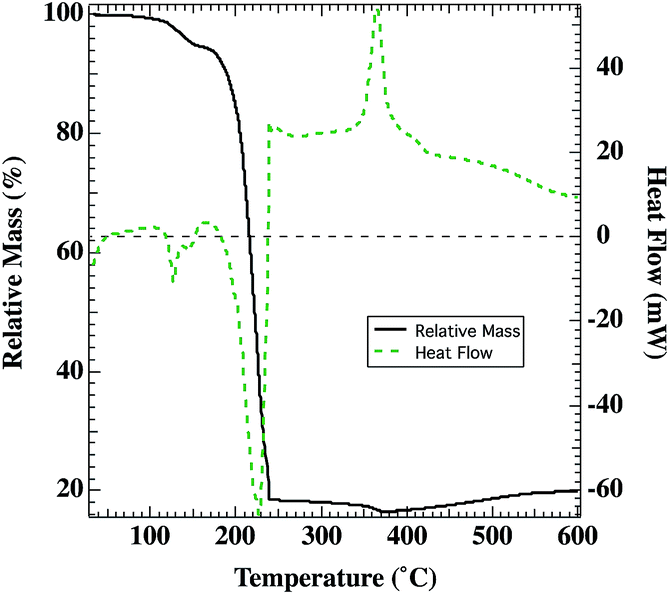 | ||
| Fig. 1 Thermal gravimetric analysis of the Ni(O2CH)2(en)2 precursor after evaporation of ethylene glycol and water (black). Differential scanning calorimetry data for the same thermal scan (green-dotted). | ||
2. Chemical composition characterization
Surface elemental composition determined from XPS measurements confirmed predominant NiOx composition as well as the presence of C and N due to the O2-plasma treatment and ambient exposure prior to measurement (see Table 1). O2-plasma is known to remove adventitious organic compounds. However, the N content in the films likely originates from the ethylenediamine, which decreases as the anneal temperature increases from 150 °C to 250 °C. Yet, after correcting for the C 1s binding energy (BE) the BE values for N 1s peak centroids are located at 406.6 eV (see S1†) and are too high to be explained by the presence of unreacted amine groups. A more likely assignment consistent with the O2-plasma treatment is one or more forms of near surface N–O species such as –NO3, which can be identified using vibrational spectroscopy.| Anneal T (°C) | Ni (%) | O (%) | C (%) | N (%) | O/Ni | Φ w (eV) |
|---|---|---|---|---|---|---|
| 150 | 33 | 55 | 8 | 4 | 1.7 | 5.4 |
| 200 | 29 | 56 | 12 | 3 | 2.0 | 5.4 |
| 250 | 27 | 60 | 11 | 2 | 2.2 | 5.5 |
| 300 | 26 | 62 | 10 | 2 | 2.4 | 5.5 |
Exposure of the NiOx thin films to O2-plasma predominantly affects the exposed surface creating similar structures for all the films while providing less effect on the subsurface material. We analyzed FTIR spectra taken for NiOx thin films to understand the O2-plasma effects for the whole system. FTIR spectra are shown in Fig. 2 for films spin-coated from the Ni(O2CH)2–en–eg–water ink, comparing the as-deposited film (‘no anneal’) to films annealed for one hour in air at 150 °C, 200 °C, 250 °C or 300 °C. Band assignments for chemical constituents of the film precursor are listed in Table 2. The major band assignments reported in the literature for the fundamental vibrations of the formate group in nickel formate (dihydrate) are the ν1ν(CH) mode at ca. 2900 cm−1, the intense ν4νas(COO) mode at ca. 1570 cm−1, and asymmetric deformation (ν5δ(C–H)) and symmetric stretch (ν2νs(COO)) modes between 1400–1350 cm−1.34,51–53 For liquid ethylene glycol, the major band assignments reported in the literature are the strong ν(OH) stretching mode at 3400–3150 cm−1, the strong asymmetric (νas(CH)) and symmetric (νs(CH)) stretch modes at 2935 cm−1 and 2875 cm−1 respectively, the strong δ(CH2) mode at ca. 1450 cm−1, and the very strong ν(CO) and ν(CC) modes at 1100–1050 cm−1.54,55 IR spectra have not been reported for the complex Ni(O2CH)2(en)2. However, literature reports indicate the major band assignments for ethylenediamine ligands in Ni(acetylacetonates)2en56 and [Ni(succinate)(en)]·2H2O49 complexes to be the asymmetric (νas(NH)) and symmetric (νs(NH)) modes at 3350–3150 cm−1, the strong δ(NH2) mode at 1613 cm−1, the ω(NH2) mode at 1318 cm−1, and the strong ν(CN) mode at 1025 cm−1. These ethylenediamine ligand band assignments for Ni complexes are consistent with values reported for other transition metal organometallic complexes56–58 and also liquid ethylenediamine.59
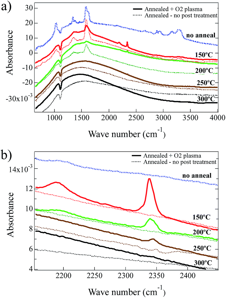 | ||
| Fig. 2 FTIR results for spin-coated (NiOx) thin films on Si wafers, comparing without anneal and annealed conditions (150 °C, 200 °C, 250 °C and 300 °C). Films that received O2-plasma treatment are indicated. Spectra are offset in order to clearly show the spectral changes. | ||
| Wavenumber (cm−1) | Assignment | Source of vibration | Reference |
|---|---|---|---|
| 1018 | ν(CN) | Ethylenediamine (ligand) | 1–3 |
| 1027 | ν(CO) | Ethylene glycol | 4 and 5 |
| 1338 | ω(NH2) | Ethylenediamine (ligand) | 2 and 3 |
| 1371 | ν 5 δ(CH) ν2νs(COO) | Formate | 6–9 |
| 1458 | δ(CH2) | Ethylene glycol | 4 and 5 |
| 1587 | ν 4 ν as(COO) | Formate | 6–9 |
| 1627 | δ(NH2) | Ethylenediamine (ligand) | 1–3 |
| 2190 | ν(CN) | Cyanate/isocyanate | 10–13 |
| 2340 | ν 3 ν as(CO2) | CO2 | 14–16 |
| 2884 | ν 1 ν(C–H) | Formate | 6–9 |
| ν s(CH) | Ethylene glycol | 4 and 5 | |
| 2936 | ν as(CH) | Ethylene glycol | 4 and 5 |
| ν(CH2) | Ethylenediamine | 1 and 2 | |
| 3300–3160 | ν(OH) | Ethylene glycol | 4 and 5 |
| 3313 | ν s(NH), νas(NH) | Ethylenediamine (ligand) | 1–3 and 17 |
| 3570 | ν(OH) | surface hydroxyls, Ni(OH)2 | 18–20 |
The bands at ca. 1020–1030 cm−1 (ν(CN) and ν(CO)) and ca. 3200–3350 cm−1 (ν(OH)) indicate ethylene glycol and/or ethylenediamine,54,55,57,59,60 and are discernible only in the no-anneal film and the film annealed at 150 °C as shown in Fig. 2a. The FTIR spectra indicate that ethylene glycol and ethylenediamine are virtually eliminated by a one hour anneal in air at 200 °C. Bands at 1627 cm−1 (δ(NH2)), and 1338 cm−1 (ν5δ(C–H)) and (ν2νs(COO)) and 1587 cm−1 (ν4νas(COO)), also seen in Fig. 2a, indicate ethylenediamine and formate respectively.34,51–53,57,59,60 The formate bands are present in the FTIR spectra for the as spun film and the films annealed at 150 °C or 200 °C without an O2-plasma treatment. A one hour anneal in air at 250 °C and 300 °C eliminates the formate from the films resulting in a near featureless spectra consistent with NiOx except for broad bands at ca. 3570 cm−1 that are surface hydroxyls.61–63 This result is consistent with the TGA/DSC data described above.
A comparison of the impact of the O2-plasma treatment, typically used for NiO HTLs, is also included in Fig. 2a and b for films annealed for one hour in air at 150 °C, 200 °C, 250 °C or 300 °C. The intensities of all the ethylenediamine, ethylene glycol, and formate bands were lowered significantly after treatment with O2-plasma, consistent with an O2-plasma being highly efficient at removing organic compounds from materials and surfaces. After O2-plasma treatment, two new bands emerge in the FTIR spectra located at 2190 cm−1 and 2340 cm−1. The 2190 cm−1 band is present after O2-plasma treatment in the film annealed at 150 °C (i.e., before the ethylenediamine is eliminated), and is very weak in the film annealed at 200 °C. The 2340 cm−1 band is present in the films annealed at 150 °C, 200 °C and 250 °C after O2-plasma treatment, although the intensity decreases significantly with increasing temperature consistent with greater conversion decomposition/oxidation of the precursor to NiOx. Given the oxidizing environment in the O2-plasma and the presence of C and N in the partially decomposed/oxidized films annealed at 150 °C and 200 °C, the 2190 cm−1 band is tentatively assigned to the ν(C–N) modes for oxygen-bonded cyanate (OCN) groups or nitrogen-bonded isocyanate (NCO) groups to Ni2+: rather than the stretch modes of C![[double bond, length as m-dash]](https://www.rsc.org/images/entities/char_e001.gif) N in a carbon nitride film.64 For example, ν(CN) modes have been reported at ca. 2200 cm−1 for the nickel isocyanate complex [Et4N]2[Ni(NCO)4],65 CNO− intercalated in α-Ni(OH)2 (ref. 66) and a theoretical study of the adsorption of cyanate and isocyanate on a Ni(100) surface;67 and at 2262 cm−1 and 2200 cm−1 for Ni(NCO)2·H2O,68 In contrast, a theoretical study of the adsorption of cyanide on a Ni(100) surface reported the ν(CN) mode at only ca. 2000 cm−1,69 and experimentally the ν(CN) mode for Ni(CN)2·2H2O was reported at 2172 cm−1.70 The 2340 cm−1 band is tentatively assigned to the ν3νas(CO2) mode of CO2 trapped in the films annealed at 150 °C–200 °C after O2-plasma treatment of the partially decomposed/oxidized Ni(O2CH)2(en)2 complex. Similar IR bands have been reported for free CO2 trapped during the thermal decomposition in air of hexahydrated nickel iron citrate to form ultrafine NiFe2O4 particles (2320 cm−1),71 propanol/TaCl5 gel to form Ta2O5 thin films (at 2345 cm−1 and 2333 cm−1),72 and zinc acetate dihydrate/sodium hydrogen carbonate mixtures in argon to form ZnO nanoparticles (at ca. 2340 cm−1).73 Both of these modes appear to be eliminated after O2-plasma treatment for the film annealed at 300 °C since decomposition/oxidation of the precursor to NiOx is complete. However, as described above a small percentage of N is still observed in the XPS spectra with high BE values for O2-plasma treated films, most likely due to near surface N–O species such as –NO3. For nickel nitrate the strong –NO3 ion stretching band would appear at ca. 1300–1400 cm−1.74–76 This is also the region where medium strength formate and ethylenediamine bands are anticipated. Confirmation of nitrate cannot be provided by the FTIR spectra after 150 °C anneal and O2-plasma treatment. However, the peak position of the ethylenediamine ω(NH2) mode shifts from 1338 cm−1 to 1358 cm−1 for the as-deposited, and 150 °C anneal plus O2-plasma respectively, and may indicate possible spectral contribution from –NO3 ions (see S2†). After the 200 °C anneal and O2-plasma treatment, the 1300–1400 cm−1 region is nearly featureless.
N in a carbon nitride film.64 For example, ν(CN) modes have been reported at ca. 2200 cm−1 for the nickel isocyanate complex [Et4N]2[Ni(NCO)4],65 CNO− intercalated in α-Ni(OH)2 (ref. 66) and a theoretical study of the adsorption of cyanate and isocyanate on a Ni(100) surface;67 and at 2262 cm−1 and 2200 cm−1 for Ni(NCO)2·H2O,68 In contrast, a theoretical study of the adsorption of cyanide on a Ni(100) surface reported the ν(CN) mode at only ca. 2000 cm−1,69 and experimentally the ν(CN) mode for Ni(CN)2·2H2O was reported at 2172 cm−1.70 The 2340 cm−1 band is tentatively assigned to the ν3νas(CO2) mode of CO2 trapped in the films annealed at 150 °C–200 °C after O2-plasma treatment of the partially decomposed/oxidized Ni(O2CH)2(en)2 complex. Similar IR bands have been reported for free CO2 trapped during the thermal decomposition in air of hexahydrated nickel iron citrate to form ultrafine NiFe2O4 particles (2320 cm−1),71 propanol/TaCl5 gel to form Ta2O5 thin films (at 2345 cm−1 and 2333 cm−1),72 and zinc acetate dihydrate/sodium hydrogen carbonate mixtures in argon to form ZnO nanoparticles (at ca. 2340 cm−1).73 Both of these modes appear to be eliminated after O2-plasma treatment for the film annealed at 300 °C since decomposition/oxidation of the precursor to NiOx is complete. However, as described above a small percentage of N is still observed in the XPS spectra with high BE values for O2-plasma treated films, most likely due to near surface N–O species such as –NO3. For nickel nitrate the strong –NO3 ion stretching band would appear at ca. 1300–1400 cm−1.74–76 This is also the region where medium strength formate and ethylenediamine bands are anticipated. Confirmation of nitrate cannot be provided by the FTIR spectra after 150 °C anneal and O2-plasma treatment. However, the peak position of the ethylenediamine ω(NH2) mode shifts from 1338 cm−1 to 1358 cm−1 for the as-deposited, and 150 °C anneal plus O2-plasma respectively, and may indicate possible spectral contribution from –NO3 ions (see S2†). After the 200 °C anneal and O2-plasma treatment, the 1300–1400 cm−1 region is nearly featureless.
FTIR analysis suggests the trapping of CO2 and the formation of N-based anions in the films annealed at the lower temperatures and after an O2-plasma treatment. The confinement of CO2 in solid-state NiOx films implies that a dense surface barrier forms during the O2-plasma treatment. The cyanate species assigned in the FTIR spectra were not identified in the more surface-sensitive XPS measurements. Moreover, nitrates observed by XPS could not be unambiguously identified with FTIR. These complementary surface and through-film measurements lead to the tentative hypothesis that the low concentration of nitrates are most likely surface confined.
3. Characterization using spectroscopic ellipsometry
In order to study the effect of annealing on the optical properties we employed angular dependent UV-vis reflection using spectroscopic ellipsometry. Fig. 3 displays the square of absorbance versus incident photon energy. Absorbance was calculated using the extinction coefficient from Lorentz oscillator model fits to the ellipsometric data. The onset of absorption was extrapolated after a linear fit to the square of the absorption coefficient between 4.1 and 4.4 eV.77 For the lowest temperature anneal at 150 °C the NiOx absorbance is low and barely resembles the absorption edge of a semiconductor, which is consistent with the minimal decomposition/oxidation of the Ni(O2CH)2(en)2 complex at this temperature. Nevertheless, fitting the onset region results in an estimate for the optical gap of 3.4 eV. For the film annealed at 200 °C, the absorbance increases as the precursor has partially decomposed/oxidized resulting in a 3.8 eV estimate of the optical band gap. For films annealed at 250 °C and 300 °C, because the decomposition of the Ni(O2CH)2(en)2 complex to NiOx is well advanced the absorption edge is more clearly defined and results in an optical gap estimate of 3.9 eV, which is in good agreement with the accepted band gap of 4.0 eV for NiO.78,79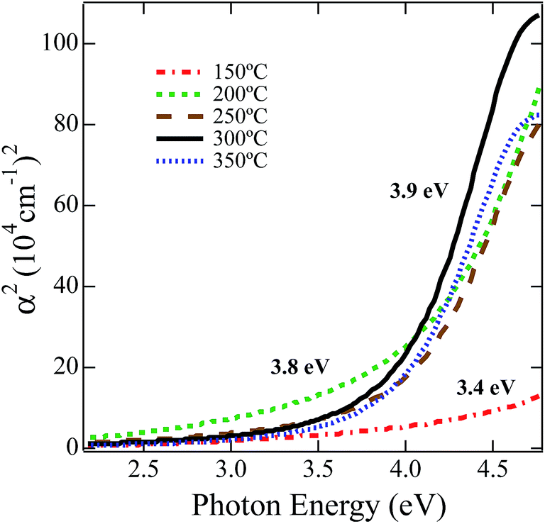 | ||
| Fig. 3 Square of absorption coefficient plot calculated with n and k measured from spectroscopic ellipsometry versus photon energy. Linear fits were obtained between 4.1 and 4.4 eV for (NiOx) films at each anneal temperature. | ||
4. OPV device performance
To investigate the impact of the NiOx film composition as a function of annealing temperature, on OPV performance we utilized these films as HTLs, annealed at different temperatures on ITO and integrated them into ITO/NiOx/PCDTBT:PC70BM/Ca/Al OPV devices. Current–voltage (JV) measurements were performed under one-sun illumination. The data from these devices are shown in Fig. 4a with calculated performance metrics in Tables 3 and 4.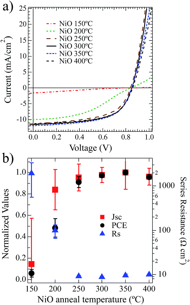 | ||
| Fig. 4 (a) Current–voltage response of PCDTBT:PC70BM solar cells with increasing anneal temperatures for the (NiOx) films spin-coated from the Ni(O2CH)2–en–eg–water solution. (b) Short circuit current (Jsc – squares) and power conversion efficiency (PCE – circles) normalized and plotted for the current–voltage curves in (a). Rs taken as the inverse slope at +1.5 V is plotted on the right axis. Error bars represent one standard deviation. | ||
| Anneal temp (°C) | V oc (mV) | ± | J sc (mA cm−2) | ± | FF | ± | PCE (%) | ± | R s – dark (Ω cm2) | ± |
|---|---|---|---|---|---|---|---|---|---|---|
| 150 | 842 | 6 | 1.7 | 0.7 | 0.23 | 0.04 | 0.3 | 0.2 | 1955.1 | 1397.9 |
| 200 | 834 | 11 | 9.8 | 0.3 | 0.35 | 0.05 | 2.8 | 0.5 | 98.6 | 33.7 |
| 250 | 850 | 14 | 11.2 | 0.2 | 0.57 | 0.04 | 5.3 | 0.3 | 9.3 | 0.4 |
| 300 | 852 | 10 | 11.5 | 0.1 | 0.59 | 0.01 | 5.6 | 0.1 | 8.7 | 0.2 |
| 350 | 852 | 7 | 11.7 | 0.3 | 0.58 | 0.00 | 5.7 | 0.1 | 9.7 | 0.6 |
| 400 | 860 | 8 | 11.2 | 0.1 | 0.59 | 0.00 | 5.5 | 0.1 | 10.1 | 0.3 |
| Anneal temp | V oc norm | J sc norm | FF norm | PCE norm | R s norm |
|---|---|---|---|---|---|
| 150 | 0.98 | 0.14 | 0.38 | 0.06 | 1.0000 |
| 200 | 0.97 | 0.84 | 0.59 | 0.48 | 0.0504 |
| 250 | 0.99 | 0.96 | 0.96 | 0.91 | 0.0047 |
| 300 | 0.99 | 0.98 | 1.00 | 0.97 | 0.0045 |
| 350 | 0.99 | 1.00 | 0.99 | 1.00 | 0.0049 |
| 400 | 1.00 | 0.96 | 1.00 | 0.96 | 0.0051 |
Power conversion efficiencies (PCE) are shown normalized in Fig. 4b and increased from 0.5% to 5.7% with increasing anneal temperature between 150 °C and 250 °C. These PCE values trend directly with short-circuit current density and as a function of thermal annealing temperature. Likewise, the PCE and Jsc inversely trend with Rs as a function of annealing temperature. For the lowest annealing temperatures (150 °C and 200 °C) the devices suffer from large resistive losses, poor current extraction and low fill factors. At 250 °C and above the Rs drops substantially and the device performance improves with gains in Jsc and FF. This drop in series resistance within the device is commensurate with the decomposition/oxidation of the NiOx layer.
It is important to note that the open-circuit voltages do not appear to trend with annealing temperature. Ultraviolet photoelectron spectroscopy (UPS) measurements (see S3†) for these solution-deposited NiOx films after annealing between 150 °C and 300 °C all produce films with very similar work function values that range from 5.4 to 5.5 eV and IP values of 5.7–5.8 ± 0.1 eV, in agreement with earlier reports.15 This is consistent with the relatively uniform Voc found across the devices when one considers work-function and the interface electronic structure of the contact determining factors of Voc. For the devices annealed at 250 °C and above there is very little statistically significant difference in the device data. As shown in Table 3, there is a modest increase just above the statistical noise from 250 °C to 300 °C. It is clear that the compositional changes from annealing the NiOx HTL to 250 °C significantly alter the electronic properties and result in enhanced hole-collection from the BHJ.
5. Conductive tip-AFM
To examine the charge transport across the NiOx films processed at different temperatures and to better understand hole-collecting efficiency, samples were prepared (in an identical way to the films used in devices) on Au as opposed to ITO substrates. Gold was used to eliminate underlying effects of electrical heterogeneity of the ITO, compared to the uniform and stable background provided on the gold surface. The nanoscale topography and electrical transport of these films were measured with conductive tip-AFM using a Pt/Ir tip held at the same tip bias for all films. For these experiments the tip forms the top contact on the Au-NiOx-Pt/Ir tip junction. Fig. 5 shows AFM and c-AFM data for five different anneal temperatures between 150 °C and 350 °C. The white pixels in the bottom row of Fig. 5 indicate a good electrical transport or an Ohmic junction, while dark pixels indicate poor electrical conductivity or diode like behavior. Since all the NiOx films have similar work functions as seen in Table 1, we can assume minimal changes in tip-surface injection/extraction barriers. Hence, we conclude that the measured c-AFM data is indicative of changes in the conductivity of the NiOx. Conformal, thin-film coatings were observed for each annealing condition on the Au substrates. Moreover, XRD analysis of a series of NiOx thin-films heated from 150 °C to 350 °C showed no sign of diffraction peaks. The 150 °C anneal resulted in an undulating surface topology (1.46 nm RMS) and a highly insulating film with no current transfer between tip and the Au ground. In contrast, the film annealed at 200 °C has a much flatter surface morphology (0.46 nm RMS) and a small but measurable current, which indicates improved charge transfer with <10% area being electrically active. As the annealing temperature is increased from 200 °C to 350 °C, increases in the NiOx film roughness and electrical property are observed. After the 250 °C anneal, the film roughness is 0.65 nm RMS and conductive regions occupy most of the surface. The 300 °C anneal results in a NiOx film with larger protrusions (1.35 nm RMS) and a sharp increase in the measured current that saturated the 20 nA c-AFM detection limit. The NiOx films resulting from a 350 °C anneal exhibits slightly lower conductivity compared to the 300 °C film, and a further increase in particle/grain size. The improved through-film conductivity, as assessed by the area of the saturated pixels, correlate well with lowering of the series resistance and improved current collection for the OPV devices. This suggests that high series resistance for the lower anneal temperatures is a result of the poor conductivity of the HTL, which is a direct result of incomplete precursor decomposition/oxidation.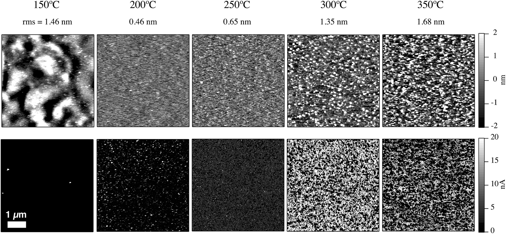 | ||
| Fig. 5 AFM (top row) and cAFM (bottom row) of NiOx films deposited on Au. From left-to-right, anneals at 150 °C, 200 °C, 250 °C, 300 °C and 350 °C for the spin-coated films. RMS roughness is stated below the corresponding anneal temperature. | ||
The large volume fraction of incompletely decomposed precursor results in resistive properties at the nanoscale and macroscale. However, separating improvements to carrier concentration and mobility remains elusive. One would expect that the improved conductivity with annealing temperature occurs due to increases of both mobility and carrier concentrations as the precursor decomposes and formation of NiO proceeds. Note that the formation of new species (cyanate, isocyanate, or nitrate) after exposing the low temperature (150 °C–200 °C) annealed films to O2-plasma, may also contribute to the poor semiconductor properties of these films. However, solution-deposited NiOx HTLs annealed at 250 °C–400 °C, and hence above the decomposition/oxidation temperature of the Ni(O2CH)2(en)2 complex, exhibit compositional changes that improve the nanoscale conductivity. These NiOx thin films can then effectively collect photogenerated holes from the BHJ with minimal resistive loss. The sub-stoichiometric nature of the NiOx produced at low annealing temperatures suggests that in addition to establishing a high work-function, the O2-plasma treatment required for optimal device performance oxidizes the NiOx but to a large extent is limited to the surface of the HTL. If the Ni(O2CH)2(en)2 is not completely decomposed (anneal temperature <240 °C), then the O2-plasma treatment does not significantly improve the NiO stoichiometry and electrical transport, and instead affects only the near surface of the thin film.
Conclusions
Thermal annealing in air and subsequent O2-plamsa treatment of solution-deposited NiOx films spin-coated from a Ni(O2CH)2–en–eg–water ink have been investigated to gain an understanding of their composition and properties in relation to hole collection in PCDTBT:PC70BM solar cells. The impacts of incomplete precursor decomposition on OPV device performance are investigated with the main effect arising as increased series resistance and concomitant lowering of short circuit current. For annealing temperatures of 150 °C–200 °C, below the decomposition temperature of the Ni(O2CH)2(en)2 complex, BHJ solar cells incorporating these ‘NiOx’ HTLs have low Jsc and high Rs. TGA identified a lower limit of 240 °C anneal temperature that is required to ensure adequate decomposition/oxidation of the Ni(O2CH)2(en)2 complex. The resulting formation of NiOx HTLs with ∼3.9 eV optical gap and adequate conductivity permits efficient hole collection in BHJ devices. TGA/DSC analysis suggests such films are initially sub-stoichiometric NiOx, which helps to explain the improved performance for subsequent O2-plasma treatment to obtain a high work function and improved film stoichiometry. Results are consistent with recent reports of other NiOx precursor formulations that produce NiOx HTLs with similar device properties at low decomposition temperature.28 These studies show increased series resistance as a direct result of incomplete decomposition of the NiOx precursor complex and how these resistive HTL films lead to lower Jsc in devices with concomitant performance loss.However, for interlayers where conversion to NiOx is performed below the decomposition temperature and is incomplete, Voc remains at high values. The surface chemistry and work function of the NiOx interlayer determines the Voc in OPV devices whether or not the organometallic precursor has fully decomposed to form NiOx. In comparison, non-selective self-assembled molecular interlayer contacts provide paths to electron transfer from the BHJ LUMO levels and reduce quasi-EF splitting, which lead to lower Voc.7 From the results presented here, we conclude that the nanoscale electrical changes as a function of converted precursor observed seem to strongly affect the ability of charge selective NiOx interlayers to extract holes from the adjacent BHJ and transport those to the external circuit. Recently, the surface polarity of NiOx interlayers was investigated and shown to dominate the interface properties when compared to the interlayer surface roughness and crystal structure.40 Hence, post treatment and formation of a dipolar surface with low defects is related to the increased polar component of the total surface energy. Data presented here shows that surface composition for these films are similar. However, differences in their nanoscale conductivity do not strongly affect the Voc. Hence, surface recombination velocity is not significantly enhanced as quasi-EF splitting seems nominally equivalent for these devices at Voc, which is consistent with steady-state and transient photocurrent studies on similar systems.42 We hypothesize that the majority of Jsc loss observed as the processing temperature is lowered below the precursor decomposition threshold proceeds via recombination in the BHJ and is not mediated by NiOx surface states. If this postulate holds, then charge selectivity and efficient carrier transport are functionally separate and proceed by different mechanisms for this particular active layer. Moreover, these properties are also spatially separate as the selectivity is determined by the surface composition and local density of states that provide a low defect interface and low surface recombination while the interlayer subsurface enables charge delocalization and carrier transport to the transparent electrode. Implications for the separation of selectivity and transport mechanisms could result in designs for bilayer selective contacts and indeed examples exist in literature.80 This can also help to decouple surface and subsurface effects of decomposition temperature, organometallic precursor formulations and subsequent surface modifications for efficient interlayer contacts in photovoltaic technologies. However in more demanding photovoltaic systems with higher carrier mobilities and photogenerated charge densities, it may be necessary to increase the NiOx thickness in order to effectively passivate high carrier density electrodes such as TCOs and metals.
Acknowledgements
Thank you Professor Reuben T. Collins at the Colorado School of Mines for thoughtful discussions. Research supported as part of the Center for Interface Science: Solar Electric Materials, an Energy Frontier Research Center funded the U.S. Department of Energy, Office of Science, Basic Energy Sciences, under Award Number DE-SC0001084 (NRA, ELR, RER, KXS), and NREL LDRD Number ARE21000.Notes and references
- E. L. Ratcliff, B. Zacher and N. R. Armstrong, J. Phys. Chem. Lett., 2011, 2, 1337–1350 CrossRef CAS.
- C. Brabec, S. Gowrisanker, J. Halls, D. Laird, S. Jia and S. Williams, Adv. Mater., 2010, 22, 3839–3856 CrossRef CAS PubMed.
- J. Chen, H. Wei and K. Ho, Sol. Energy Mater. Sol. Cells, 2007, 91, 1472–1477 CrossRef CAS PubMed.
- H. Frohne, S. Shaheen, C. J. Brabec, D. Muller, N. Sariciftci and K. Meerholz, ChemPhysChem, 2002, 9, 795–799 CrossRef.
- S. Khodabakhsh, B. Sanderson, J. Nelson and T. Jones, Adv. Funct. Mater., 2006, 16, 95–100 CrossRef CAS PubMed.
- P. Ndione, A. Garcia, E. Widjonarko, A. K. Sigdel, K. X. Steirer, D. C. Olson, P. A. Parilla, D. S. Ginley, N. R. Armstrong, R. E. Richards, E. L. Ratcliff and J. J. Berry, Adv Energy Mater, 2013, 3, 524–531 CrossRef CAS PubMed.
- E. L. Ratcliff, A. Garcia, S. A. Paniagua, S. R. Cowan, A. J. Giordano, D. S. Ginley, S. R. Marder, J. J. Berry and D. C. Olson, Adv. Energy Mater., 2013, 3, 647–656 CrossRef CAS PubMed.
- E. L. Ratcliff, J. Meyer, K. Steirer, N. R. Armstrong, D. C. Olson and A. Kahn, Org. Electron., 2012, 13, 744–749 CrossRef CAS PubMed.
- J. Meyer and A. Kahn, Proc. SPIE, 2011, 1, 1–7 Search PubMed.
- J. Meyer, A. K. Zilberberg, T. Riedl and A. Kahn, J. Appl. Phys., 2011, 110, 033710 CrossRef PubMed.
- J. H. Seo, S. Cho, M. Leclerc and A. J. Heeger, Chem. Phys. Lett., 2011, 503, 101–104 CrossRef CAS PubMed.
- H. Ishii, K. Sugiyama, E. Ito and K. Seki, Adv. Mater., 1999, 11, 605–625 CrossRef CAS.
- N. R. Armstrong, P. A. Veneman, E. L. Ratcliff, D. Placencia and M. Brumbach, Acc. Chem. Res., 2009, 42, 1748–1757 CrossRef CAS PubMed.
- T. Ripolles-Sanchis, A. Guerrero, E. Azaceta, R. Tena-Zaera and G. Garcia-Belmonte, Sol. Energy Mater. Sol. Cells, 2013, 117, 564–568 CrossRef CAS PubMed.
- J. Reinhardt, M. Grein, C. Bühler, M. Schubert and U. Würfel, Adv. Energy Mater., 2014 DOI:10.1002/aenm.201400081 Search PubMed.
- M. Bolognesi, A. Sánchez-Díaz, J. Ajuria, R. Pacios and E. Palomares, Phys. Chem. Chem. Phys., 2011, 13, 6105–6109 RSC.
- M. Irwin, D. Buchholz, A. Hains, R. Chang and T. Marks, Proc. Natl. Acad. Sci. U. S. A., 2008, 105, 2783–2787 CrossRef CAS.
- F. Liu, S. Shao, X. Guo, Y. Zhao and Z. Xie, Sol. Energy Mater. Sol. Cells, 2010, 94, 842–845 CrossRef CAS PubMed.
- V. Shrotriya, G. Li, Y. Yao, C.-W. Chu and Y. Yang, Appl. Phys. Lett., 2006, 88, 073508 CrossRef PubMed.
- K. X. Steirer, P. F. Ndione, N. E. Widjonarko, M. T. Lloyd, J. Meyer, E. L. Ratcliff, A. Kahn, N. R. Armstrong, C. J. Curtis, D. S. Ginley, J. J. Berry and D. C. Olson, Adv. Energy Mater., 2011, 1, 813–820 CrossRef CAS PubMed.
- M. D. Irwin, J. D. Servaites, D. Buchholz, B. Leever, J. Liu, J. Emery, M. Zhang, J. Song, M. Durstock, A. Freeman, M. Bedzyk, M. Hersam, R. Chang, M. Ratner and T. Marks, Chem. Mater., 2011, 23, 2218–2226 CrossRef CAS.
- J. Zhang, J. Wang, Y. Fu, B. Zhang and Z. Xie, J. Mater. Chem. C, 2014, 2, 8295–8302 RSC.
- V. Wood, M. J. Panzer, J. E. Halpert, J. M. Caruge, M. G. Bawendi and V. Bulović, ACS Nano, 2009, vol. 3, 3581–3586 CrossRef PubMed.
- B. S. Mashford, T.-L. Nguyen, G. J. Wilson and P. Mulvaney, J. Mater. Chem., 2009, 20, 167 RSC.
- J.-Y. Jeng, K.-C. Chen, T.-Y. Chiang, P.-Y. Lin, T.-D. Tsai, Y.-C. Chang, T.-F. Guo, P. Chen, T.-C. Wen and Y.-J. Hsu, Adv. Mater., 2014, 26, 4107–4113 CrossRef CAS PubMed.
- W. Chen, Y. Wu, J. Liu, C. Qin, X. Yang, A. Islam, Y.-B. Cheng and L. Han, Energy Environ. Sci., 2015, 8, 629–640 CAS.
- L. Hu, J. Peng, W. Wang, Z. Xia, J. Yuan, J. Lu, X. Huang, W. Ma, H. Song, W. Chen, Y.-B. Cheng and J. Tang, ACS Photon., 2014, 1, 547–553 CrossRef CAS.
- J. R. Manders, S.-W. Tsang, M. J. Hartel, T.-H. Lai, S. Chen, C. M. Amb, J. R. Reynolds and F. So, Adv. Funct. Mater., 2013, 23, 2993–3001 CrossRef CAS PubMed.
- J. Jung, D. L. Kim, S. H. Oh and H. J. Kim, Sol. Energy Mater. Sol. Cells, 2012, 102, 103–108 CrossRef CAS PubMed.
- K. X. Steirer, J. P. Chesin, N. E. Widjonarko, J. J. Berry, A. Miedaner, D. S. Ginley and D. C. Olson, Org. Electron., 2010, 11, 1–5 CrossRef PubMed.
- V. Zardetto, T. M. Brown, A. Reale and A. Di Carlo, J. Polym. Sci., Part B: Polym. Phys., 2011, 49, 638–648 CrossRef CAS PubMed.
- A. A. Balandin, E. S. Grigoryan and Z. S. Yanysheva, Acta Physicochim. URSS, 1940, 12, 737–758 CAS.
- L. L. Bircumshaw and J. Edwards, J. Chem. Soc., 1950, 1800–1809 RSC.
- G. R. Rao, K. C. Patil and C. N. R. Rao, Inorg. Chim. Acta, 1970, 4, 215–218 CrossRef CAS.
- B. R. Wheeler and A. K. Galwey, J. Chem. Soc., Faraday Trans. 1, 1974, 70, 661–670 RSC.
- A. K. Galwey and M. E. Brown, Proc. R. Ir. Acad., Sect. B, 1977, 77, 465–471 Search PubMed.
- A. B. Edwards, C. D. Garner and K. J. Roberts, J. Phys. Chem. B, 1997, 101, 20–26 CrossRef CAS.
- A. H. Qusti, A. A. Samarkandy, S. Al-Thabaiti and E.-H. M. Diefallah, J. King Abdulaziz Univ., 1997, 9, 73–81 CrossRef PubMed.
- Z. Zhai, X. Huang, M. Xu, J. Yuan and J. Peng, Adv. Energy Mater., 2013, 3, 1614–1622 CrossRef CAS PubMed.
- N. E. Widjonarko, P. Schulz, P. A. Parilla, C. L. Perkins, P. F. Ndione, A. K. Sigdel, D. C. Olson, D. S. Ginley, A. Kahn, M. F. Toney and J. J. Berry, Adv. Energy Mater., 2014, 4, 1301879 Search PubMed.
- E. L. Ratcliff, J. Meyer, K. X. Steirer, A. Garcia, J. J. Berry, D. S. Ginley, D. C. Olson, A. Kahn and N. R. Armstrong, Chem. Mater., 2011, 23, 4988–2000 CrossRef CAS.
- S. R. Cowan, J. V. Li, D. C. Olson and E. L. Ratcliff, Adv. Energy Mater., 2014, 5, 1400549 Search PubMed.
- G. Narain, Bull. Chem. Soc. Jpn., 1966, 39, 2298–2300 CrossRef CAS.
- N. Armstrong, C. Carter, C. Donley, A. Simmonds, P. Lee, M. Brumbach, B. Kippelen, B. Domercq and S. Yoo, Thin Solid Films, 2003, 445, 342–352 CrossRef CAS PubMed.
- M. P. Seah, Surf. Interface Anal., 1989, 14, 488–488 CrossRef CAS PubMed.
- M. Ghaemy, A. Omrani and A. Rostami, J. Appl. Polym. Sci., 2005, 97, 265–271 CrossRef CAS PubMed.
- H. Icbudak, T. K. Yazicilar and W. T. Yilmaz, Thermochim. Acta, 1999, 335, 93–98 CrossRef CAS.
- K. S. Rejitha and S. Mathew, J. Therm. Anal. Calorim., 2010, 102, 931–939 CrossRef CAS.
- V. T. Yilmaz, S. Demir, O. Andac and W. T. A. Harrison, J. Coord. Chem., 2002, 55, 863–872 CrossRef CAS.
- K. S. Rejitha and S. Mathew, J. Therm. Anal. Calorim., 2008, 93, 213–217 CrossRef CAS.
- H. G. Edwards and A. Knowles, J. Mol. Struct., 1992, 268, 13–22 CrossRef CAS.
- F. J. A. Garcia and M. M. P. Manrique, Ion, 1976, 36, 422–425 Search PubMed.
- D. Stoilova and V. Koleva, Spectrochim. Acta, Part A, 2001, 57, 2629–2636 CrossRef CAS.
- P. D. Buckley and P. A. Giguere, Can. J. Chem., 1967, 45, 397–407 CrossRef CAS.
- W. Sawdony, K. Niedenzu and J. W. Dawson, Spectrochim. Acta, Part A, 1967, 23, 799–806 CrossRef.
- J. A. Broomhead and L. A. P. Kane-Maguire, J. Chem. Soc. A, 1967, 4, 546–553 RSC.
- T. Iwamoto and D. F. Shriver, Inorg. Chem., 1971, 10, 2428–2432 CrossRef CAS.
- J. J. A. McLean, A. F. Schreiner and A. F. Laethem, J. Inorg. Nucl. Chem., 1964, 26, 1245–1248 CrossRef CAS.
- A. Sabatini and S. Califano, Spectrochim. Acta, 1960, 16, 677–688 CrossRef CAS.
- M. L. Niven and G. C. Percy, Transition Met. Chem. (Dordrecht, Neth.), 1978, 3, 267–271 CrossRef CAS.
- J. L. Bantignies, S. Deabate, A. Righi, S. Rols, P. Hermet, J. L. Sauvajol and F. Henn, J. Phys. Chem. C, 2008, 112, 2193–2201 CAS.
- N. Bellakhal and J. L. Brisset, J. Chem. Res., Synop., 2001, 238–239 CrossRef CAS.
- D. S. Hall, D. J. Lockwood, S. Poirier, C. Bock and B. R. MacDougall, J. Phys. Chem. A, 2012, 116, 6771–6784 CrossRef CAS PubMed.
- L. Escobar-Alarcon, A. Arrieta, E. Camps, S. Romero and M. A. Camacho-Lopez, Superficies Vacio, 2005, 18, 9–12 Search PubMed.
- D. Forster and D. M. L. Goodgame, J. Chem. Soc., Jan., 1965, 262–267 Search PubMed.
- B. Mavis and M. Akinc, Chem. Mater., 2006, 18, 5317–5325 CrossRef CAS.
- H. Yang and J. L. Whitten, Surf. Sci., 1998, 401, 313–321 CrossRef.
- R. Micu-Semeniuc and C. G. Macarovici, Rev. Roum. Chim., 1972, 17, 981–992 CAS.
- H. Yang and J. L. Whitten, Journal of Chem. Phys., 1997, 107, 8518–8524 CrossRef CAS PubMed.
- A. Ludi and R. Huegi, Helv. Chim. Acta, 1968, 51, 349–355 CrossRef CAS PubMed.
- N. S. Gajbhiye and S. Prasad, Thermochim. Acta, 1996, 285, 325–336 CrossRef CAS.
- J. Kristof, A. D. Battisti, G. Keresztury, E. Horvath and T. Sziligyi, Langmuir, 2001, 17, 1637–1640 CrossRef CAS.
- W. M. H. Oo, M. D. McCluskey, A. D. Lalonde and M. G. Norton, Appl. Phys. Lett., 2005, 86, 073111 CrossRef PubMed.
- E. L. Williams, R. A. Bailey and S. E. Wberley, J. Inorg. Nucl. Chem., 1970, 32, 2197–2203 CrossRef CAS.
- T. J. Taylor, D. Dollimore, G. A. Gamlen, A. J. Barnes and M. A. Stuckey, Thermochim. Acta, 1986, 101, 291–304 CrossRef CAS.
- S. Srinivasan and S. Ganguly, Catal. Lett., 1991, 10, 279–288 CrossRef CAS.
- F. Urbach, Phys. Rev., 1953, 1324 CrossRef CAS.
- A. Fujimori and F. Minami, Phys. Rev. B: Condens. Matter Mater. Phys., 1984, 30, 957–971 CrossRef CAS.
- S. Hüfner, Adv. Phys., 1994, 43, 183–356 CrossRef.
- J. D. Zimmerman, B. Song, O. Griffith and S. R. Forrest, Appl. Phys. Lett., 2013, 103, 243905 CrossRef PubMed.
Footnotes |
| † Electronic supplementary information (ESI) available: XPS of N 1s, UPS and additional FTIR for NiOx films. See DOI: 10.1039/c5ta01379h |
| ‡ Present address: Intel Corporation, Portland, OR, USA. |
| § Present address: Next Energy Technologies Inc. Santa Barbara, CA, USA. |
| ¶ Present address: Washington Nanofabrication Facility at the University of Washington, Seattle WA, USA. |
| This journal is © The Royal Society of Chemistry 2015 |