
 Open Access Article
 This Open Access Article is licensed under a Creative Commons Attribution-Non Commercial 3.0 Unported Licence
TiO2 enhanced ultraviolet detection based on a graphene/Si Schottky diode†
Miao
Zhu
ab,
Li
Zhang
a,
Xinming
Li
c,
Yijia
He
ab,
Xiao
Li
ab,
Fengmei
Guo
a,
Xiaobei
Zang
a,
Kunlin
Wang
a,
Dan
Xie
*d,
Xuanhua
Li
e,
Bingqing
Wei
ef and
Hongwei
Zhu
*ab
aSchool of Materials Science and Engineering, State Key Laboratory of New Ceramics and Fine Processing, Tsinghua University, Beijing 100084, China. E-mail: hongweizhu@tsinghua.edu.cn
bCenter for Nano and Micro Mechanics, Tsinghua University, Beijing 100084, China
cNational Center for Nanoscience and Technology, Zhongguancun, Beijing 100190, China
dTsinghua National Laboratory for Information Science and Technology (TNList), Institute of Microelectronics, Tsinghua University, Beijing 100084, China. E-mail: xiedan@tsinghua.edu.cn
eSchool of Materials Science and Engineering, Northwestern Polytechnical University, Xi'an 710072, China
fDepartment of Mechanical Engineering, University of Delaware, Newark, DE 19716, USA
First published on 11th March 2015
Abstract
Graphene/Si has been proved to form a quality Schottky junction with high photoelectric conversion efficiency at AM 1.5. However, for the ultraviolet portion of the incident light, the photoelectric performance will degrade significantly due to severe absorption and recombination at the front surface. Herein, to realize enhanced ultraviolet detection with a graphene/Si diode, TiO2 nanoparticles (NPs, 3–5 nm) are synthesized and spin-coated on the graphene surface to improve the photoresponse in the ultraviolet region. According to our results, the conversion efficiency of the graphene/Si diode at 420 nm and 350 nm increases by 72.7% and 100% respectively with TiO2 coating. Then C−2–V measurements of both TiO2 and graphene/Si diode are performed to analyze the electronic band structure of the TiO2/graphene/Si system, based on which we finally present the enhancement mechanism of photodetection using TiO2 NPs.
Introduction
As a highly conductive and transparent material, graphene has been considered as a promising material in energy conversion.1–4 Solar cells and photodetectors based on graphene/Si Schottky heterojunctions have been widely reported in previous studies as two types of typical photovoltaic devices based on graphene.5–12 Such devices possess a very simple structure with graphene lying on the surface of an n-type silicon substrate. In such structures, the Richardson constant of Si can be significantly lowered due to the finite density of states of graphene and thus results in a low leakage current, which has been proved using the Landauer transport model.13 Once the incident light arrives at the graphene/Si interface, carriers are excited and then separated by the built-in electric field to achieve the photoelectrical conversion process. A solar cell with such a structure was first reported with an initial power conversion efficiency (PCE) of around 1.5%.14 In the following five years, various approaches have been employed to improve its efficiency, including chemical doping,15–17 structural design,18–20 and electrolyte assistance.21 In a recent study by our group, TiO2 antireflection coating and acid doping were performed together to improve the PCE to 14.5% at AM 1.5, nearly ten times higher than the initially reported level.22The approaches applied above are quite valuable to enhance the photoresponse properties of graphene/Si based photodetectors. However, being different from a solar cell, the photodetector mainly focuses on the response of light within a certain wavelength range. The photoelectric conversion from different light wavelengths can hardly be reflected by the investigation of solar cells. For example, ultraviolet will be strongly absorbed by the front surface of the device, resulting in severe recombination and thermal loss. Despite the fact that the PCE of the graphene/Si diode can be improved at AM 1.5, the ultraviolet response maybe still far lower than that in its optimal wavelength region. Thus it is meaningful to enhance the ultraviolet response of the graphene/Si diode to widen its effective working spectrum range.
Introducing a functional layer for light absorption and conversion is a widely used method to improve photovoltaic devices,23–28 and it is especially suitable to enhance the photoresponse and PCE of ultraviolet for the graphene/Si diode according to the above analysis. TiO2 is a common photocatalytic material with strong absorbance in the ultraviolet range.29–32 When irradiated by ultraviolet, excitons generated in TiO2 may be used to enhance the response of the graphene/Si diode via carrier injection. This is quite different from the case of long-wavelength light which is mainly based on the optical antireflection of TiO2. In this work, the ultraviolet detection of the graphene/Si diode is greatly improved by simply spin-coating a layer of TiO2 nanoparticles (NPs) on the surface of the device. The performances of the device before and after TiO2 coating, including the current density–voltage (J–V) characteristics, responsivity, quantum efficiency, etc., were compared to show the effects of the TiO2 layer. The band diagram of the TiO2/graphene/Si system was then deduced from the C−2–V characteristics and finally a possible enhancement mechanism of the TiO2 layer was presented.
Experimental
Synthesis of TiO2 NPs
TiO2 was synthesized by a nonhydrolytic sol–gel approach described as follows: after stirring a solution of TiCl4 (1 mL), ethanol (5 mL), and benzyl alcohol (35 mL) for 6 h at 80 °C, it was washed with diethyl ether three times. A white TiO2 precipitate was obtained by centrifuging the crude product. The final TiO2 solution was prepared by dispersing it in ethanol.Preparation of graphene
Multilayer graphene (MLG) was prepared by an atmospheric chemical vapor deposition method. Copper foil (25 μm, 99.8%, purchased from Alfa Aesar Chemical Co. Ltd.) was placed in a tube furnace for use as the substrate. Under the protection of Ar (200 mL min−1) and H2 (30 mL min−1), the furnace was heated to 1000 °C in 50 min and further maintained for 30 min. Methane (20 mL min−1) was then fed in as the carbon source. After 15 min reaction, the copper substrate was quickly moved away from the heating zone and cooled down to room temperature. The copper substrate was then immersed in 0.5 M FeCl3 and graphene was successively transferred to deionized water and rinsed thoroughly to clean the residual FeCl3 and other impurities.Fabrication of the device
MLG was directly transferred onto an n-type silicon substrate with a SiO2 layer along its surface borders (window area is ∼0.1 cm2). After drying in air, TiO2 NPs dispersed in ethanol (0.2 mg mL−1) were spin-coated on the surface of graphene at 2000 rpm for 30 s, as illustrated in Fig. 1a. Silver paste and the deposited Ti/Au layer were used as the top electrode and back electrode of the device, respectively. A typical photograph of the device (without electrodes) is shown in Fig. 1b.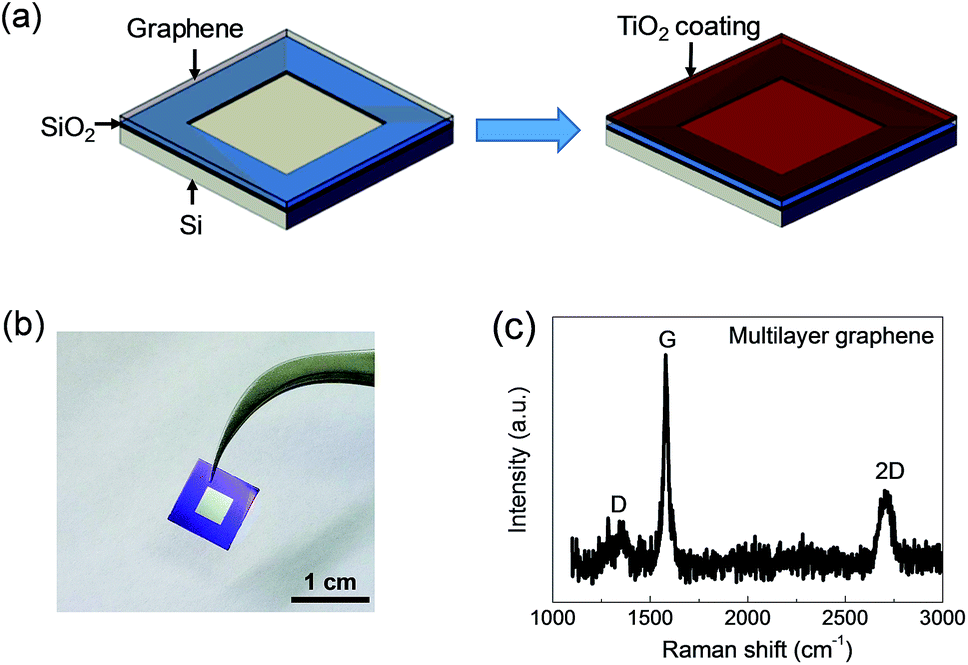 | ||
| Fig. 1 (a) Schematic of the device fabrication. (b) Photograph of the device. (c) Raman spectrum of the multilayer graphene. I2D/IG ≈ 0.34. | ||
C −2–V measurement
C −2–V measurement for TiO2 NPs was performed with a Potentiostat (CHI 660D) using a three-electrode system. The Ag/AgCl and platinum electrodes were used as the reference and counter electrodes, respectively. TiO2 NPs were spin-coated on an FTO coated glass to fabricate the working electrode. H2SO4 aqueous solution (0.5 M) was used as the electrolyte. The applied AC potential was 1 kHz with an amplitude of 0.01 V. Electrode potentials were converted to NHE using the relationship VNHE = VAg/AgCl + 0.197 V. For the MLG/Si diode, both the reference and counter electrodes were connected with the top electrode of the device, and the working electrode was connected with its back electrode. The frequency and amplitude of the applied AC voltage are 5 kHz and 0.01 V, respectively.Characterization
Raman spectra were recorded on a HORIBA LabRAM HR Evolution with a 514 nm laser source. Scanning Electron Microscopy (SEM) was performed on a Zeiss Merlin compact. Transmission Electron Microscopy (TEM) was performed on a JEM-2010 TEM. The UV-Vis spectrum of graphene was measured using an Agilent Cary 5000. Atomic Force Microscopy (AFM) was tested using an Agilent N9451A. The thickness of the TiO2 layer was measured by KLA Tencor Surface Profilometry. The J–V and on/off characteristics were recorded on a Keithley 2601. The X-ray photoelectron spectrum (XPS) was collected on an XPS 250XI.Results and discussion
In order to enhance the ultraviolet response of the MLG/Si diode, a TiO2 layer was coated on the surface of graphene to utilize the light energy irradiated on the device more efficiently. In the TiO2/MLG/Si sandwich system, graphene functioned not only as the functional layer to form Schottky junctions with both the Si substrate and TiO2 layer, but also acted as the conductive layer through which the carriers transport to the external circuit. Fig. S1† shows that the transmittance of the MLG was about 86.9% (at 550 nm). According to the 2.3% linear optical absorption of monolayer graphene to white light,33 it could be deduced that as-synthesized MLG was about 6-layered, which was consistent with its Raman spectrum (I2D/IG ≈ 0.34, Fig. 1c).34,35 The metallic impurities in graphene may significantly influence the diode behavior of the MLG/Si device.13 The XPS study was performed to investigate the metallic impurities in as-prepared graphene samples. The results (Fig. S2†) show a quite low atomic percentage of Fe and Cu, the most possible metallic impurities introduced into graphene during preparation and transfer processes.The morphology of TiO2 NPs has a great influence on their improvement effects. Poorly dispersed particles and thick bulk agglomeration will severely affect the carrier diffusion and separation, as well as reduce the light energy arriving at the MLG/Si interface. The TEM image (Fig. 2a) reveals that the TiO2 NPs were well-dispersed with an average size of 3–5 nm. The high resolution TEM (HRTEM) image further shows the lattice fringes of TiO2 NPs. The inter-planar distance of 0.24 nm and 0.35 nm correspond to the (004) and (101) planes of anatase TiO2. After being coated on MLG, the TiO2 NPs were uniformly spread on the MLG surface without an obvious discontinuous region such as cracks or holes, as shown in the SEM image (Fig. 2b).
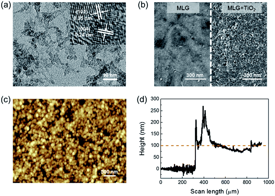 | ||
| Fig. 2 (a) TEM image of TiO2 NPs. The mean size of TiO2 NPs is about 3–5 nm. The inset shows a typical HRTEM image of TiO2 NPs. (b) SEM images of MLG before (left) and after (right) TiO2 coating. (c) AFM image of the TiO2 layer. (d) Height changes from MLG to the TiO2 layer. The thickness of the TiO2 layer is about 100 nm. | ||
AFM was further performed to characterize the morphology of the TiO2 layer, as shown in Fig. 2c. It can be observed that the TiO2 NPs are self-assembled into spherical agglomerations with larger sizes. Even so, the distribution of the agglomerated TiO2 NPs still remains uniform in general. The thickness of the TiO2 layer was measured by Surface Profilometry, and the results (Fig. 2d) showed that the average thickness of the TiO2 layer was about 100 nm.
The J–V relationship is the most important and widely used characteristic for diode performance. J–V characteristics of the devices were measured under a beam of 420 nm incident light with the intensity of 0.16 W cm−2 (Fig. 3a). It can be deduced that the initial photoelectrical conversion efficiency of the device is only 0.44%. After being coated with TiO2 NPs, the PCE increased to 0.76%, nearly 1.7 times higher than that of the original value. The open circuit voltage (Voc) of the device was nearly stable, but the short circuit current density (Jsc) increased apparently, which contributed much to the increase of PCE. Acid doping has been reported to be another efficient way to improve the PCE of the MLG/Si device.7,9 The TiO2 coated device was then exposed to HNO3 (analytical reagent) vapor for about 30 s. The blue curve in Fig. 3a shows that the acid doping still worked efficiently in improving the PCE after being coated with TiO2 NPs. The probable reason was that the HNO3 vapor could permeate through the channels formed between TiO2 NP agglomerations to arrive at the surface of graphene and then cause doping effects. Being different from the only TiO2 NP coating, it can be seen from Fig. 3a that the increase of Voc and fill factor (FF) contributed the most part of the PCE improvement in the case of acid doping. This indicated that the enhancement mechanism of TiO2 NPs was different from the doping effect of HNO3. The obvious increase of Jsc after TiO2 coating was probably because that the TiO2 NPs could provide extra excited carriers when ultraviolet irradiated on the surface. This was also consistent with the band gap of TiO2 (about 3.0–3.2 eV, corresponding to the wavelength of 388–413 nm).36,37 The band gap of nanoparticles was relevant to their sizes and crystal structures.38,39 The actual excited wavelength limit might fall in a wider range around 413 nm. As an example for the light with higher energy, J–V characteristics of the device at 350 nm incident light (2.21 W cm−2) were also tested (Fig. S3†). The PCE of the device increased by 100% (from 0.065% to 0.13%) after TiO2 coating, higher than the case at 420 nm. The dark J–V characteristics (Fig. 3b) show that neither TiO2 coating nor acid doping would significantly affect the rectification behavior of the MLG/Si diode.
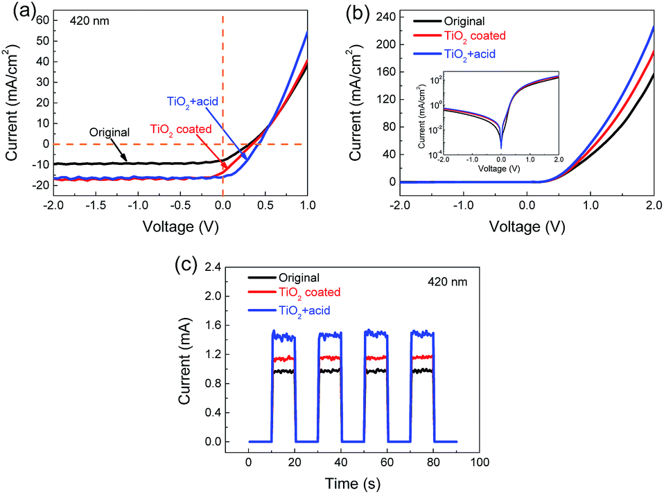 | ||
| Fig. 3 (a) Light and (b) dark current–voltage characteristics of the device. The inset shows corresponding log-linear plots. (c) On/off characteristics of the device tested at 420 nm incident light. | ||
Response current is another important parameter of a photodetector because it is usually used directly as the response or output signal of the device. On/off characteristic measurements were performed and the results are shown in Fig. 3c. Thanks to the improvement of PCE, the response current (Iresp) at 420 nm increased from 0.97 to 1.15 mA, and finally reached 1.47 mA after acid doping. The TiO2 coated device shows excellent repeatability of switching behavior (Fig. S4†) in 10 min. The response and recovery time are measured to be 1.30 ms and 2.76 ms, respectively (Fig. S5†), which are comparable to the values of graphene/Si photodetectors reported previously.5 In addition, the thickness effect of the TiO2 layer on device performance has been discussed in Fig. S6.† The performance tested under different conditions is summarized in Table 1 to clearly show the improvements and differences.
| Structure | V oc (mV) | J sc (mA cm−2) | FF (%) | PCEUV (%) | I resp (mA) | Responsivity (mA/W) |
|---|---|---|---|---|---|---|
| Original | 300 | 7.11 | 32.78 | 0.44 | 0.97 | 60.6 |
| TiO2 coated | 300 | 12.02 | 33.87 | 0.76 | 1.15 | 71.9 |
| TiO2 + acid | 400 | 15.12 | 40.25 | 1.52 | 1.47 | 91.9 |
To investigate the behavior of the TiO2 layer in a wider spectral range, the quantum efficiency was measured from 300 to 1100 nm. The results (Fig. 4) show that the quantum efficiency in the near-ultraviolet range was obviously improved after TiO2 coating.
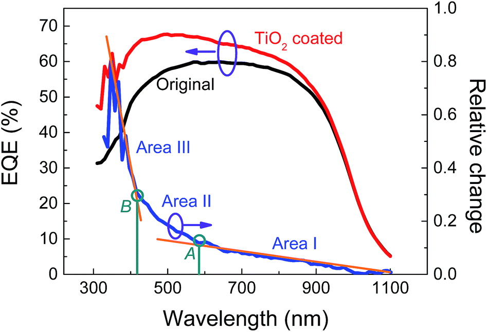 | ||
| Fig. 4 External quantum efficiency (EQE) of the device before and after TiO2 coating. The blue curve shows the relative changes. | ||
In order to illustrate more clearly, the relative change of quantum efficiency (ΔEQE) was calculated by (EQETiO2 coated − EQEoriginal)/EQEoriginal and is shown as the blue curve in Fig. 4, which can be divided into three typical areas (areas I to III) along with the decrease of the light wavelength. In area I, from 1100 nm to point A (570 nm), ΔEQE increased mildly from 0.01 to 0.12. The photon energy of the light in this area was too low to excite the electrons in TiO2, so the enhancement mechanism was mainly possible to be optical antireflection. In area II, from point A to point B (410 nm), ΔEQE turned out to increase more quickly, indicating that parts of the TiO2 NPs could be excited by the incident light to generate carriers, which contributed to the increase of ΔEQE. When the photon energy further increased (wavelength < point B), the carriers could be excited abundantly in the TiO2 layer, resulting in a sharp increase of the ΔEQE. It is worth mentioning that light with too short wavelength may lose most of its energy in the TiO2 layer and seldom photons can arrive at the MLG/Si interface, thus a peak value of ΔEQE may exist in area III. According to the above analysis, the quantum efficiency of the device in the whole range from 300 to 1100 nm can be improved continuously by TiO2 coating based on both optical antireflection and carrier injection from the TiO2 layer.
Similar to the MLG/Si side, the excited electron (e−)–hole (h+) pairs in the TiO2 layer should be separated by a suitable built-in voltage. Thus the investigation of the band structure of the TiO2/MLG/Si system is critical to support our above analysis. The band structure was investigated by a two-step method based on the C−2–V measurements.
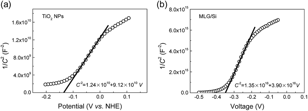
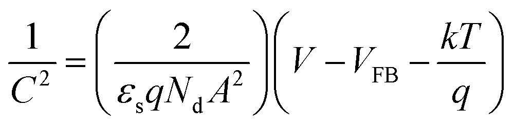
In detail, the band structures of TiO2/MLG and MLG/Si were first measured individually and then combined to be a whole picture of the sandwich system, assuming that the weak influences between each other could be neglected. The measurements for TiO2 NPs were based on a three-electrode system. TiO2 NPs were spin-coated on an FTO coated glass and tested in 0.5 M H2SO4 aqueous solution. The results are shown in Fig. 5a. By fitting the linear region of the C−2–V plots, the x-intercept (V0) was found to be −0.136 V.
 | ||
| Fig. 5 C −2–V characteristics of (a) TiO2 NPs and (b) MLG/Si Schottky diode. | ||
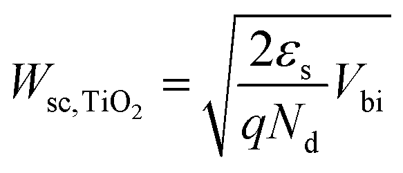
Then the experimental carrier concentration and flat-band potential of TiO2 NPs were calculated from the Mott–Schottky equation:40
 | (1) |
 | (2) |
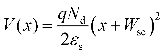
The calculated Wsc,TiO2 was 2.89 nm. The potential change along the thickness direction of the depletion layer was also confirmed by
 | (3) |
Then the band structure of TiO2/graphene was deduced as shown in the left part of Fig. 6a. To measure the C−2–V characteristics of the MLG/Si side, both the reference electrode and counter electrode were connected with MLG, while the working electrode was connected with the back electrode of the device. In the same way, Nd,Si, VFB,Si and Wsc,Si were calculated to be 3.08 × 1016 cm−3, −0.373 V and 125.5 nm, respectively. The V(x) in the MLG/Si side was calculated by eqn (3). Therefore, the band diagram of the whole TiO2/MLG/Si system was deduced and is shown in Fig. 6a.
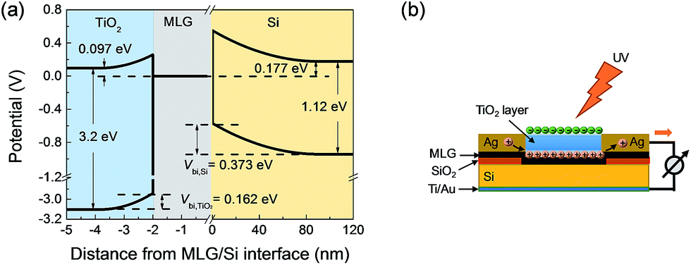 | ||
| Fig. 6 (a) Band diagram of the TiO2/MLG/Si system. (b) Schematic of the performance enhancement mechanism by TiO2 coating. | ||
It can be seen that there are two built-in voltages existing in the TiO2/MLG/Si system: one lies at the TiO2/MLG interface and another lies at the MLG/Si interface. Once the incident light arrived at the TiO2 layer, photons with energy higher than the band gap of TiO2 were absorbed to excite the electrons of TiO2 from its valance band to the conduction band, then the photo-generated electron–hole pairs were separated by the built-in voltage. The photo-generated holes (h+) can be transported towards graphene together with the current generated from the MLG/Si side to the external circuit. However, as TiO2 is a wide band gap dielectric material with poor conductivity, the photo-generated electrons (e−) have to remain in the TiO2 layer through capacitive coupling with the holes (Fig. 6b), which is similar to the model presented before for a graphene-quantum dot phototransistor.43 Despite the fact that the carrier concentration of TiO2 was much high than that of silicon, its enhancement effect might be limited by such mechanisms, because too much electrons accumulated on the surface of the TiO2 layer would enhance their recombination with the holes.
Conclusions
In summary, TiO2 NPs were synthesized to enhance the ultraviolet photoelectrical conversion of the MLG/Si diode. After being coated by TiO2 NPs, the PCE of the device obviously improved (increased by 72.7% and 100% at 420 nm and 350 nm respectively). The EQE characteristics revealed that the enhancement mechanism of the TiO2 layer in the ultraviolet region was different from the long-wave region. Next, the band diagram of the TiO2/MLG/Si system was established using the Mott–Schottky theory according to its C−2–V characteristics, which confirmed that there existed two reciprocal Schottky junctions in the sandwich system. The enhancement mechanism was finally attributed to the carrier injection from the TiO2 layer to the loop current of graphene/semiconductor based on the electronic band structure.Acknowledgements
This work is supported by the National Science Foundation of China (51372133) and Tsinghua National Laboratory for Information Science and Technology (TNList) Cross-discipline Foundation. X. H. Li thanks the support of start-up funds from Northwestern Polytechnical University. The authors thank for the microscopy resource provided by the Beijing National Center for Electron Microscopy.Notes and references
- F. Bonaccorso, L. Colombo, G. Yu, M. Stoller, V. Tozzini, A. C. Ferrari, R. S. Ruoff and V. Pellegrini, Science, 2015, 347, 1246501 CrossRef PubMed.
- L. Dai, Acc. Chem. Res., 2013, 46, 31 CrossRef CAS PubMed.
- I. V. Lightcap and P. V. Kamat, Acc. Chem. Res., 2013, 46, 2235 CrossRef CAS PubMed.
- H. Wang, H. Feng and J. Li, Small, 2014, 10, 2165 CrossRef CAS PubMed.
- X. An, F. Liu, Y. J. Jung and S. Kar, Nano Lett., 2013, 13, 909 CrossRef CAS PubMed.
- P. Lv, X. Zhang, X. Zhang, W. Deng and J. Jie, IEEE Electron Device Lett., 2013, 34, 1337 CrossRef CAS.
- J. Kim, S. S. Joo, K. W. Lee, J. H. Kim, D. H. Shin, S. Kim and S. Choi, ACS Appl. Mater. Interfaces, 2014, 6, 20880 CAS.
- X. Gan, R. Shiue, Y. Gao, I. Meric, T. F. Heinz, K. Shepard, J. Hone, S. Assefa and D. Englund, Nat. Photonics, 2013, 7, 883 CrossRef CAS.
- X. Wang, Z. Cheng, K. Xu, H. K. Tsang and J. Xu, Nat. Photonics, 2013, 7, 888 CrossRef CAS.
- A. Pospischil, M. Humer, M. M. Furchi, D. Bachmann, R. Guider, T. Fromherz and T. Mueller, Nat. Photonics, 2013, 7, 892 CrossRef CAS.
- M. Amirmazlaghani, F. Raissi, O. Habibpour, J. Vukusic and J. Stake, IEEE J. Quantum Electron., 2013, 49, 589 CrossRef CAS.
- C. Liu, Y. Chang, T. B. Norris and Z. Zhong, Nat. Nanotechnol., 2014, 9, 273 CrossRef CAS PubMed.
- D. Sinha and J. U. Lee, Nano Lett., 2014, 14, 4660 CrossRef CAS PubMed.
- X. Li, H. Zhu, K. Wang, A. Cao, J. Wei, C. Li, Y. Jia, Z. Li, X. Li and D. Wu, Adv. Mater., 2010, 22, 2743 CrossRef CAS PubMed.
- X. Miao, S. Tonga, M. K. Petterson, K. Berke, A. G. Rinzler, B. R. Appleton and A. F. Hebard, Nano Lett., 2012, 12, 2745 CrossRef CAS PubMed.
- T. Cui, R. Lv, Z. Huang, S. Chen, Z. Zhang, X. Gan, Y. Jia, X. Li, K. Wang, D. Wu and F. Kang, J. Mater. Chem. A, 2013, 1, 5736 CAS.
- H. Kim, K. Lee, N. McEvoy, C. Yim and G. S. Duesberg, Nano Lett., 2013, 13, 2182 CrossRef CAS PubMed.
- G. Fan, H. Zhu, K. Wang, J. Wei, X. Li, Q. Shu, N. Guo and D. Wu, ACS Appl. Mater. Interfaces, 2011, 3, 721 CAS.
- L. Yang, X. Yu, M. Xu, H. Chen and D. Yang, J. Mater. Chem. A, 2014, 2, 16877 CAS.
- K. Jiao, X. Wang, Y. Wang and Y. Chen, J. Mater. Chem. C, 2014, 2, 7715 RSC.
- X. Li, X. Zang, X. Li, M. Zhu, Q. Chen, K. Wang, M. Zhong, J. Wei, D. Wu and H. Zhu, Adv. Energy Mater., 2014, 4, 1400224 Search PubMed.
- E. Shi, H. Li, L. Yang, L. Zhang, Z. Li, P. Li, Y. Shang, S. Wu, X. Li, J. Wei, K. Wang, H. Zhu, D. Wu, Y. Fang and A. Cao, Nano Lett., 2013, 13, 1776 CAS.
- D. H. Lee, J. Y. Kwon, S. Maldonado, A. Tuteja and A. Boukai, Nano Lett., 2014, 14, 1961 CrossRef CAS PubMed.
- C. Li, C. Chueh, H. Yip, K. M. O'Malley, W. Chen and A. K.-Y. Jen, J. Mater. Chem., 2012, 22, 8574 RSC.
- A. Shalav, B. S. Richards and M. A. Green, Sol. Energy Mater. Sol. Cells, 2007, 91, 829 CrossRef CAS PubMed.
- Z. Su, L. Wang, Y. Li, G. Zhang, H. Zhao, H. Yang, Y. Ma, B. Chu and W. Li, ACS Appl. Mater. Interfaces, 2013, 5, 12847 CAS.
- Z. Wu, T. Song, Z. Xia, H. Wei and B. Sun, Nanotechnology, 2013, 24, 484012 CrossRef PubMed.
- M. Xu, X. Zhu, X. Shi, J. Liang, Y. Jin, Z. Wang and L. Liao, ACS Appl. Mater. Interfaces, 2013, 5, 2935 CAS.
- J. Schneider, M. Matsuoka, M. Takeuchi, J. Zhang, Y. Horiuchi, M. Anpo and D. W. Bahnemann, Chem. Rev., 2014, 114, 9919 CrossRef CAS PubMed.
- S. G. Kumar and L. G. Devi, J. Phys. Chem. A, 2011, 115, 13211 CrossRef CAS PubMed.
- I. Paramasivam, H. Jha, N. Liu and P. Schmuki, Small, 2012, 8, 3073 CrossRef CAS PubMed.
- K. Nakata and A. Fujishima, J. Photochem. Photobiol., C, 2012, 13, 169 CrossRef CAS PubMed.
- G. Pirruccio, L. M. Moreno, G. Lozano and J. G. Rivas, ACS Nano, 2013, 7, 4810 CrossRef CAS PubMed.
- V. T. Nguyen, H. D. Le, V. C. Nguyen, T. T. T. Ngo, D. Q. Le, X. N. Nguyen and N. M. Phan, Adv. Nat. Sci.: Nanosci. Nanotechnol., 2013, 4, 035012 CrossRef.
- W. Wu, Z. Liu, L. A. Jauregui, Q. Yu, R. Pillai, H. Cao, J. Bao, Y. P. Chen and S. Pei, Sens. Actuators, B, 2010, 150, 296 CrossRef CAS PubMed.
- S. G. Yenchalwar, V. K. Azhagan and M. V. Shelke, Phys. Chem. Chem. Phys., 2014, 16, 17786 RSC.
- H. Ariga, T. Taniike, H. Morikawa, M. Tada, B. K. Min, K. Watanabe, Y. Matsumoto, S. Ikeda, K. Saiki and Y. Iwasaw, J. Am. Chem. Soc., 2009, 131, 14670 CrossRef CAS PubMed.
- D. Segets, J. M. Lucas, R. N. K. Taylor, M. Scheele, H. Zheng, A. P. Alivisatos and W. Peukert, ACS Nano, 2012, 6, 9021 CrossRef CAS PubMed.
- L. Li, J. Hu, W. Yang and A. P. Alivisatos, Nano Lett., 2001, 1, 349 CrossRef CAS.
- K. Cheng, C. Huang, G. Pan, P. Chen, T. Lee and T. C. K. Yang, Mater. Chem. Phys., 2008, 108, 16 CrossRef CAS PubMed.
- J. Kim, J. H. Hwang, J. Suh, S. Tongay, S. Kwon, C. C. Hwang, J. Wu and J. Y. Par, Appl. Phys. Lett., 2013, 103, 171604 CrossRef PubMed.
- K. Xu, C. Zeng, Q. Zhang, R. Yan, P. Ye, K. Wang, A. C. Seabaugh, H. G. Xing, J. S. Suehle, C. A. Richter, D. J. Gundlach and N. V. Nguyen, Nano Lett., 2013, 13, 131 CrossRef CAS PubMed.
- G. Konstantatos, M. Badioli, L. Gaudreau, J. Osmond, M. Bernechea, F. P. G. de Arquer, F. Gatti and F. H. L. Koppens, Nat. Nanotechnol., 2012, 7, 363 CrossRef CAS PubMed.
Footnote |
| † Electronic supplementary information (ESI) available: Transmission spectrum of graphene, XPS spectrum of graphene, J–V characteristics and detection performance of the device. See DOI: 10.1039/c5ta00702j |
| This journal is © The Royal Society of Chemistry 2015 |