
 Open Access Article
 This Open Access Article is licensed under a Creative Commons Attribution-Non Commercial 3.0 Unported Licence
Fatigue resistance of a flexible, efficient, and metal oxide-free perovskite solar cell†
Kianoosh
Poorkazem
,
Dianyi
Liu
and
Timothy L.
Kelly
*
Department of Chemistry, University of Saskatchewan, 110 Science Place, Saskatoon, SK S7N 5C9, Canada. E-mail: tim.kelly@usask.ca
First published on 23rd January 2015
Abstract
Although the high efficiencies of perovskite solar cells have attracted the most attention from the photovoltaic community, one of their most attractive attributes is that flexible devices can be prepared by depositing the perovskite on plastic substrates using solution-based processing techniques. Highly flexible devices have the potential to be fabricated through roll-to-roll manufacturing, which is a fast and easy method for light weight thin-film solar cell production. In order to determine the flexibility of these perovskite-based devices, we have carried out fatigue resistance measurements on flexible perovskite solar cells by bending the devices over a cylinder with a 4 mm radius of curvature for up to 2000 cycles. We show that the main reason for the drop in performance of these devices is the formation of cracks in the indium oxide-based transparent conductive electrode. To improve device flexibility, we substituted the metal oxide electrode with a layer of highly conductive poly(3,4-ethylenedioxythiophene):poly(styrene sulfonate) (PEDOT:PSS). The resulting devices were entirely metal oxide free, and displayed power conversion efficiencies as high as 7.6% with very little hysteresis. By comparing the fatigue resistances of these metal oxide-free devices with those of polymer-based solar cells, we were able to evaluate the inherent flexibility of CH3NH3PbI3 films for the first time.
Introduction
Perovskite solar cells (PSCs) have emerged as a potential alternative to silicon solar cells, which are heavy, expensive, and brittle. This brittleness does not allow for the fabrication of silicon-based devices using roll-to-roll (R2R) production. R2R manufacturing is fast and economical, making it ideal for mass-production; however, it only works well for thin-film devices that are light and flexible, and can be processed at low temperatures using solution-based processing techniques. Organic solar cells (OSCs) possess all of these characteristics, and for many years research on flexible photovoltaics has focused on this type of device. Unfortunately, the efficiencies of OSCs are modest, making them less competitive with silicon and CdTe-based devices.1 In contrast, perovskite solar cells can now be fabricated with excellent power conversion efficiencies,2–5 and with record-setting efficiencies now exceeding 17%, PSCs are increasingly competitive with silicon and CdTe-based technology.1,6 Moreover, the CH3NH3PbI3 perovskite is made from inexpensive starting materials, and many researchers have tried to decrease costs even further by using cheaper alternatives for the electron- and hole-transport layers.7,8 However, in order to encourage the commercialization of this technology, the toxicity of lead,9–12 the perovskite's sensitivity to moisture,3,10,11 and the limited flexibility of the device architecture are all issues that must be addressed.2,13–15The majority of flexible PSCs fabricated to date have been based on indium tin oxide (ITO) transparent conductive electrodes, and are fabricated using solution-based processing16 and low-temperature methods.17–19 Early work evaluated the flexibility of the perovskite solar cell by bending the device over cylinders with different radii of curvature.2 It suggested that the device flexibility was limited by the elastic limit of the ITO/PET (poly(ethylene terephthalate)) substrate and not the perovskite layer; however, no data on the fatigue resistance of the device was reported. Three important studies have been carried out since. In one, the perovskite layer was fabricated on stainless steel fibre/TiO2 substrates.20 In another, a layer of Ag was sandwiched between two layers of Al-doped ZnO on a PET substrate, and the whole was used as the transparent conductive electrode in a PSC.14 In both of these studies, the fatigue resistance of the devices was measured by bending the devices over a cylinder with a fixed radius of curvature for, at most, 50 bending cycles. Given the limited number of cycles, it is not clear if these devices are mechanically robust enough to survive the many cycles of bending necessitated by R2R manufacture, packaging, transportation, installation and use. In recent work, the fatigue resistance of a PSC was studied by bending a device to a 4 mm radius of curvature for 1000 cycles, and the failure in device performance was attributed to crack formation in the ITO layer.21 In additional work based on density functional theory, the flexibility of CH3NH3BX3 perovskites was shown to be dependent on the shear modulus and the strength of the B–X bond, and be independent of organic–inorganic ion interactions.22 In addition, the Poisson's ratio (τ) of the CH3NH3PbI3 perovskite was shown to be larger than 0.30, which places it between that of rigid glass (0.18) and rubber (0.50). These values indicate a more molecular (rather than ionic or ionic-covalent) crystal, and suggest that the perovskite possess a higher level of flexibility than conventional crystalline inorganic semiconductors. However, despite this theoretical prediction, and the studies on flexible PSCs reported to date, very little is known about the flexibility and mechanical robustness of CH3NH3PbI3 films.
The ITO electrodes predominantly used in flexible solar cell technology have a number of disadvantages which limit their utility. The scarcity and expense of indium increases the overall production cost associated with the fabrication process,23,24 and the high temperatures required to process indium-free alternatives (such as fluorine-doped tin oxide) make them unsuitable for deposition on plastic substrates. Most importantly for this work, however, is the brittleness of the metal oxide films.23,24 Their poor mechanical performance means that they are not ideal electrodes for flexible applications and R2R production. A literature report of an ITO-based transparent thin-film transistor showed that the semiconductor field effect mobility decreased to 85% of its original value after bending the device to a 2 mm radius of curvature just once.25 In another report, an ITO/PET-containing dye-sensitized solar cell was bent 1000 times around a cylinder of 7 mm radius, and the observed cracks were attributed to the inflexibility of ITO.26
Alternative transparent conductive electrodes, in addition to possessing good mechanical flexibility, must also display high transmittance and low sheet resistance.23,27,28 Very few materials possess all three of these characteristics. Metal films typically have low transmittance when they are thick,27 and low conductivity (as well as a tendency to oxidize) when they are thin.28 Silver nanowires have both high transmittance and a low sheet resistance; however, nanowire and nanofiber structures often lead to device shorting unless flattened under high pressures.29 Carbon nanotubes28 and graphene28,30–32 are other materials that have been widely used in optoelectronic devices. However, carbon nanotubes often suffer from poor charge transfer between nanotubes, and need to be fabricated in high densities.24 In contrast, highly conductive poly(3,4-ethylenedioxythiophene):poly(styrene sulfonate) (HC-PEDOT) electrodes can be prepared with low sheet resistance, high surface coverage, and high transmittance, using simple fabrication methods. They also have highly favourable mechanical properties, and have already been applied in the fabrication of highly flexible OSCs.33–38
In this report, we have fabricated both perovskite and organic solar cells on PET substrates. In comparing the fatigue resistance of the PSCs prepared using a metal oxide electrode with those prepared on HC-PEDOT, we find that cracks in the metal oxide electrode are the primary reason for device failure after repeated bending cycles. The devices prepared using HC-PEDOT are entirely metal oxide free, and display good power conversion efficiencies (up to 7.6%) with very little hysteresis. Our results further show that the perovskite film, while more flexible than the underlying metal oxide electrode, is still more prone to cracking than conventional polymer-based active layers. This has a deleterious effect on device performance, suggesting that for applications demanding high flexibility and many repeated bending cycles (e.g., textile or fabric-integrated photovoltaics), organic semiconductors remain the material of choice.
Results and discussion
Device characteristics
Fig. 1 shows the two types of flexible PSC architectures used in the current study. The first design (PET/M-In2O3/ZnO/CH3NH3PbI3/Spiro-OMeTAD/Ag, hereafter abbreviated as M-In2O3/ZnO/CH3NH3PbI3) is already established as one that yields high efficiency PSCs;2 the second architecture (PET/HC-PEDOT/SC-PEDOT/CH3NH3PbI3/PC61BM/Al, hereafter abbreviated as HC-PEDOT/SC-PEDOT/CH3NH3PbI3) is fabricated for the first time here, and introduces a HC-PEDOT layer to replace the metallized indium oxide (M-In2O3) electrode. The M-In2O3 film is a commercially available Au- and Ag-coated In2O3 layer, and has mechanical properties, transmittance, and sheet resistance qualitatively similar to a typical ITO electrode. The HC-PEDOT is expected to be substantially more flexible than the indium oxide layer, such that the mechanical properties of the perovskite film can be evaluated. It was spin-coated from a solution containing 5% (v/v) dimethyl sulfoxide and 0.5% (v/v) Zonyl F-300 fluorosurfactant,35 producing a 190 nm thick film. In both architectures, the perovskite layer is fabricated through a two-step deposition process (spin-coating a layer of PbI2, followed by immersion in a CH3NH3I solution).2,39 The absorption spectrum and pXRD pattern of the perovskite layer are shown in Fig. S1.† In both cases, the perovskite is placed between electron- and hole-transport layers: either ZnO and 2,2′,7,7′-tetrakis-(N,N-di-p-methoxyphenylamine)-9,9′-bifluorene (Spiro-OMeTAD), or [6,6]-phenyl-C61-butyric acid methyl ester (PC61BM) and semiconducting poly(3,4-ethylenedioxythiophene):poly(styrene sulfonate) (SC-PEDOT). Importantly, for the device based on the HC-PEDOT electrode, all layers (with the exception of the aluminium counter electrode) are deposited from solution by spin-coating. With a maximum processing temperature of 120 °C, these processing steps are highly compatible with R2R manufacturing processes. The thicknesses of the various device layers (as determined by profilometry) are consistent with previous literature reports of high performance devices.2,40–42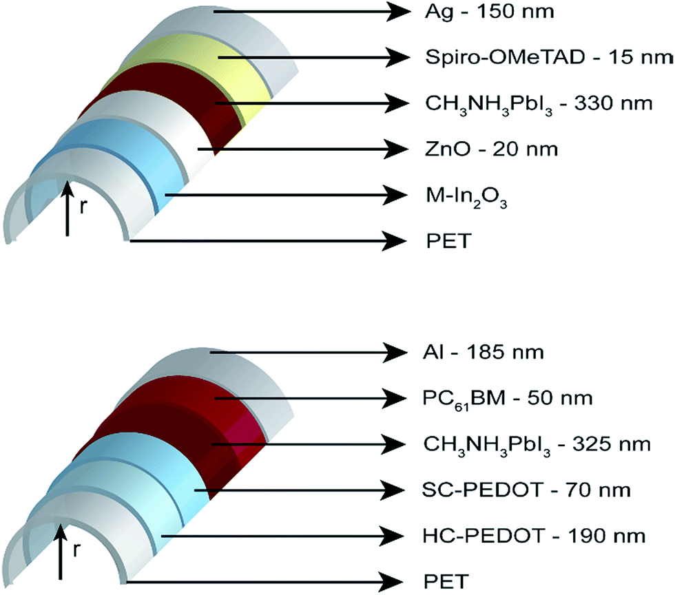 | ||
| Fig. 1 Schematic of the device architecture for M-In2O3/ZnO/CH3NH3PbI3 (top) and HC-PEDOT/SC-PEDOT/CH3NH3PbI3 (bottom) cells, bent at a radius of curvature, r. | ||
Fig. 2a shows the transmission spectrum of each transparent conductive thin film electrode. Both electrodes have similar transmittance at wavelengths <610 nm; however, at longer wavelengths, the HC-PEDOT electrode significantly outperforms the M-In2O3 analogue. At 800 nm, at the absorption onset of the perovskite, the transmittances of these electrodes are 85% and 64%, respectively. The higher transmittance for the HC-PEDOT leads to a larger portion of the light reaching the perovskite layer. This is likely to be even more significant for tandem solar cells,10,11 where the perovskite is paired with an additional red-to-near infrared absorber.
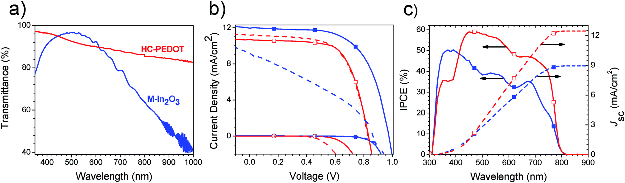 | ||
| Fig. 2 (a) Transmission spectra of M-In2O3 and HC-PEDOT electrodes, after subtraction of the PET background spectrum. (b) J–V curves of representative M-In2O3/ZnO/CH3NH3PbI3 (blue) and HC-PEDOT/SC-PEDOT/CH3NH3PbI3 (red) devices, measured from forward bias to short-circuit (solid lines), and from short-circuit to forward bias (dashed lines), in both the light (squares) and in the dark (circles). (c) IPCE spectra (solid lines) and calculated Jsc values (dashed lines) for M-In2O3/ZnO/CH3NH3PbI3 (solid blue squares) and HC-PEDOT/SC-PEDOT/CH3NH3PbI3 (open red squares) devices. | ||
The two different types of PSC were tested under AM 1.5G illumination, and Table 1 shows both the average and the best results. Comparing the results of the HC-PEDOT/SC-PEDOT/CH3NH3PbI3 cells with those of the M-In2O3/ZnO/CH3NH3PbI3 analogues, we find that there is very little difference in either the short-circuit current density (Jsc) or the fill factor (FF). Given that the perovskite films were deposited in the same way, and have similar thicknesses, the similarity in performance is perhaps unsurprising. The main difference in the two devices is the lower open-circuit voltage (Voc) of the HC-PEDOT/SC-PEDOT/CH3NH3PbI3 device. Pairwise t-tests were carried out at the 95% confidence level to statistically validate these comparisons (Table S1†). The efficiency of 7.6% for the HC-PEDOT/SC-PEDOT/CH3NH3PbI3 device is highly encouraging, as it is a first step toward combining the high efficiency of the PSCs with the high flexibility of all-organic electron- and hole-transport layers and electrodes.
| Electrode | V oc (V) | J sc (mA cm−2) | FF | PCE (%) | R s (Ω cm2) | R sh (Ω cm2) |
|---|---|---|---|---|---|---|
| M-In2O3 (average) | 0.90 ± 0.07 | 11 ± 2 | 0.51 ± 0.07 | 5 ± 2 | (3 ± 1) × 10 | (5 ± 2) × 102 |
| M-In2O3 (best) | 0.96 | 12 | 0.66 | 7.8 | 9 | 5 × 10² |
| HC-PEDOT (average) | 0.7 ± 0.2 | 11 ± 2 | 0.5 ± 0.1 | 4 ± 2 | 17 ± 7 | (1 ± 2) × 103 |
| HC-PEDOT (best) | 0.8 | 15 | 0.6 | 7.6 | 12 | 5 × 10³ |
Fig. 2b and c show the J–V curves and incident photon-to-current efficiency (IPCE) spectra for representative devices of both architectures. Hysteresis (a difference in the current response with the bias scanning direction) is a major concern in perovskite solar cells,43–45 and as such, we have investigated the hysteretic behaviour of both types of devices. As reported in Table 1, the PCEs of the best M-In2O3/ZnO/CH3NH3PbI3 and HC-PEDOT/SC-PEDOT/CH3NH3PbI3 cells were 7.8% and 7.6%, respectively. However, Fig. 2b indicates that the hysteretic effect is much less pronounced for the latter, as the J–V curves for reverse and forward directions are quite similar. In Fig. S2,† the J–V curves of representative devices are shown with various dwell times spent on each voltage step. With increasing dwell times, the reverse- and the forward-direction J–V curves become more similar, eventually becoming virtually superimposable under pseudo-steady state conditions. As a result, for relatively fast measurements, there is a discrepancy in the PCE obtained from the two scans: for the M-In2O3/ZnO/CH3NH3PbI3 device, the reverse and forward-scans yielded PCEs of 7.8% and 4.2% respectively, while for the HC-PEDOT/SC-PEDOT/CH3NH3PbI3 device, both scans produced a PCE of 7.6%.
Further insight into the hysteretic behavior of the devices can be gained from the IPCE spectra. Fig. 2c shows the IPCE spectra of the M-In2O3/ZnO/CH3NH3PbI3 and HC-PEDOT/SC-PEDOT/CH3NH3PbI3 devices, as well as the Jsc calculated by integration of the IPCE spectra with the AM 1.5G solar flux. The HC-PEDOT/SC-PEDOT/CH3NH3PbI3 device clearly outperforms the M-In2O3 counterpart in the red region of the spectrum, reflecting the improved transmission of the HC-PEDOT electrode (Fig. 2a). Furthermore, since the IPCE spectra are measured under pseudo-steady state conditions, the calculated Jsc values should provide a good representation of the actual solar cell performance.46 Both IPCE spectra in Fig. 2c were measured for devices with a Jsc of 12 mA cm−2 (as determined from the reverse scan of the J–V curve). The short-circuit current densities calculated from the IPCE spectra were 9 and 12 mA cm−2 for the M-In2O3 and HC-PEDOT/SC-PEDOT/CH3NH3PbI3 devices, respectively. The fact that the Jsc values for the M-In2O3 devices are inconsistent is in keeping with the substantial degree of hysteresis observed in these devices, whereas the excellent agreement observed for the HC-PEDOT-based cells reflects the lack of observed hysteresis. This result is significant in that many reports promote the limited hysteresis of mesoscopic PSCs as a substantial advantage over their planar heterojunction counterparts;11,45 however, here we have demonstrated that planar heterojunction devices can also be prepared with very limited hysteresis in the J–V curve. These findings are consistent with literature reports on the hysteretic behaviour of inverted architectures.19,47–51 Mitigation of hysteresis has been observed when either SC-PEDOT50 or C60-fullerenes52 have been used as charge extraction layers. This has been attributed to a low number of interfacial charge traps47,51 and (in the case of fullerene-based acceptors) to strong charge carrier extraction.52 Very recently, spin-coating of PC61BM on top of the perovskite layer was shown to passivate trap states by permeating into nano-pathways between perovskite grain boundaries. This permeation decreases the charge transport barrier and increases the charge extraction efficiency; as a result, it substantially reduces the amount of hysteresis that is observed.53 Our own observations are consistent with these findings and highlight the importance of interfacial layers on the hysteretic effect.45,49 If the HC-PEDOT devices are measured using a long dwell time at each voltage step (Fig. S2c†), the Jsc of the reverse direction is found to be slightly lower (and the Voc slightly higher) than that measured in the forward scan.
Fatigue resistance
One of the most important questions surrounding flexible PSCs is their resistance to mechanical fatigue. In order to better understand the mechanical flexibility and failure mechanisms of these PSCs, they were subjected to a lengthy fatigue test alongside two polymer-based devices with the same transparent conductive electrodes: PET/M-In2O3/ZnO/P3HT:PC61BM/SC-PEDOT/Ag (hereafter abbreviated as M-In2O3/ZnO/P3HT:PC61BM), and PET/HC-PEDOT/SC-PEDOT/P3HT:PC61BM/ZnO/Al (hereafter abbreviated as HC-PEDOT/SC-PEDOT/P3HT:PC61BM), where P3HT is poly(3-hexylthiophene). The electrical parameters of these devices are presented in Table S2.†Fatigue tests were carried out on 9 separate cells (3 cells on each of 3 separate substrates) for each of the four types of devices. The cells were bent around a cylindrical object of 4 mm radius until they either shorted or 2000 bending cycles were reached. By carrying out >1000 bending cycles, we provide a much more realistic measure of the suitability of perovskite devices for flexible photovoltaic applications than any previous work.2,14,20 The effect of repeated bending on device PCE is presented in Fig. 3, and the changes in the other electrical parameters (Voc, Jsc, FF, Rs and Rsh) as a function of the number of bending cycles are reported in Fig. S3.† As shown in Fig. 3a, the nine devices with the M-In2O3/ZnO/CH3NH3PbI3 architecture all short-circuit quite suddenly after 100 to 1100 bending cycles. The changes in the J–V curves prior to short-circuit can be seen in Fig. 3a. Although there is little change in performance for the first 100 cycles, immediately thereafter the Voc and the Jsc both decrease sharply. This is likely due to the sudden and concurrent drop in the fill factor; a sharp increase in the series resistance and a decrease in the shunt resistance lead to a roughly 60% loss in FF. Immediately thereafter, the device fails by short-circuit. In contrast, the HC-PEDOT/SC-PEDOT/CH3NH3PbI3 devices degrade by a very different mechanism (Fig. 3b). Although the PCE of the HC-PEDOT/SC-PEDOT/CH3NH3PbI3 device drops rapidly in the first 300 bending cycles (similar to many of the M-In2O3/ZnO/CH3NH3PbI3 cells), the device performance then stabilizes, and none of the nine devices shorted, even after 2000 bending cycles. In these devices, there is very little change in the Voc; instead, the Jsc gradually decreases, driven primarily by an increase in the Rs. Combined with a decrease in Rsh, this leads to a substantial loss in FF after 2000 bending cycles.
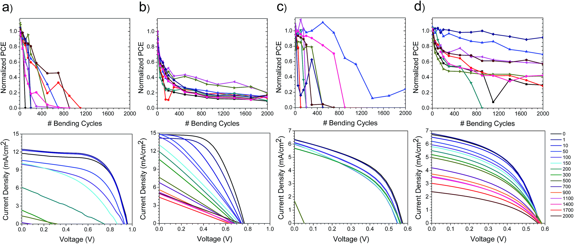 | ||
| Fig. 3 Results of the fatigue tests for the (a) M-In2O3/ZnO/CH3NH3PbI3, (b) HC-PEDOT/SC-PEDOT/CH3NH3PbI3, (c) M-In2O3/ZnO/P3HT:PC61BM, and (d) HC-PEDOT/SC-PEDOT/P3HT:PC61BM devices. The top row shows the normalized PCE for each of 9 separate devices. The bottom row shows the J–V curves as a function of the number of bending cycles for a typical device. | ||
Fig. 3c and d show the results of the fatigue test for the OSCs. The majority of the M-In2O3/ZnO/P3HT:PC61BM devices fail by short-circuit in the range of 100 to 900 bending cycles, with only one device remaining functional after 2000 cycles. The similarity of these results with those in Fig. 3a suggests that both M-In2O3/ZnO/CH3NH3PbI3 and M-In2O3/ZnO/P3HT:PC61BM devices fail by a similar degradation mechanism; this implies that changes in the M-In2O3 electrode may be the underlying reason for device failure. Despite this broad similarity, there are small differences in the rate of change in PCE. In Fig. 3a, a steady loss in PCE is observed, followed by catastrophic short-circuit, whereas in the P3HT:PC61BM devices (Fig. 3c), the initial device performance is better retained prior to a sudden device failure. This suggests that the perovskite film may be contributing to the initial drop in efficiency, with breakage of the M-In2O3 electrode being responsible for the ultimate short-circuit of the device. This theory is supported by a comparison of the fatigue resistance of the perovskite and polymer solar cells on HC-PEDOT electrodes. From Fig. 3d, it can be observed that all but one of the HC-PEDOT/SC-PEDOT/P3HT:PC61BM devices still work after 2000 bending cycles. The Voc is almost entirely unchanged throughout the test, and only a modest decrease in the fill factor is observed. The device performance does deteriorate slowly, owing almost entirely to losses in Jsc. Given the all-organic nature of this device, this level of fatigue resistance is perhaps unsurprising. The average PCEs of the HC-PEDOT/SC-PEDOT/CH3NH3PbI3 and HC-PEDOT/SC-PEDOT/P3HT:PC61BM devices after 2000 bending cycles were 15 ± 4% and 50 ± 30% of their initial values, respectively. Given that the same transparent conductive electrode was used in both cases, this is further evidence that the perovskite layer appears to be less flexible than polymer-based semiconductors.
In order to further probe the limitations on the flexibility of these devices, three devices of each type were subjected to single bending cycles at increasingly sharp radii of curvature (Fig. S4†). In a manner analogous to the fatigue tests, the devices with the M-In2O3 electrodes fail by short-circuit after being bent to radii of less than 2 mm. In contrast, devices based on the HC-PEDOT electrodes do not fail by short-circuit, and instead display a continual loss of efficiency as the radius of curvature is lowered. Again, the perovskite-based device shows a more rapid decline in efficiency, with a noticeable loss in performance beginning at a 4 mm bend radius. In contrast, the HC-PEDOT/SC-PEDOT/P3HT:PC61BM devices maintain ∼75% of their initial performance up to a bend radius of 2 mm. Bending the devices to radii of less than 1.2 mm exceeds the elastic limit of the PET substrate, and so more severe radii of curvature were not tested.
In order to probe the origins of the observed device degradation, sheet resistance measurements were carried out on both the M-In2O3 and HC-PEDOT electrodes. Five electrodes of each type were tested with a four-point probe prior to any mechanical deformation. After bending one electrode of each type for 2000 cycles, the sheet resistance was measured again. The sheet resistances of the M-In2O3 and the HC-PEDOT electrodes were measured to be 8.1 ± 0.2 Ω □−1 and 104 ± 5 Ω □−1, respectively. After bending, the sheet resistance of the M-In2O3 film was beyond the measurement range of the instrument; however, the resistance of the HC-PEDOT electrode increased only marginally, to 113 Ω □−1. This increase in the sheet resistance of the M-In2O3 electrode is attributed to the brittleness of the metal oxide matrix, which is clearly not an issue for the HC-PEDOT electrode. Fig. 4 shows a scanning electron micrograph of this breakage and the effect that it has on the top perovskite layer. Control images of pristine electrodes (before bending) are shown in Fig. S5.† As can be seen in Fig. 4a, after 2000 bending cycles, a series of large cracks are created on the surface of the M-In2O3 electrode, which prevent charge transport and lead to the dramatic increase in sheet resistance described previously. These cracks can then propagate through the perovskite film (Fig. 4b), and are observed as either horizontal, white-edged lines (where they have broken through to the surface of the perovskite layer), or dark streaks (where the crack is localized below the surface). These breaks lead to short-circuits and, ultimately, device failure. In contrast, Fig. 4c shows no evidence of crack formation in the HC-PEDOT electrode, which is consistent with the negligible change in the sheet resistance. The surface texture visible in Fig. 4c is a result of the roughness of the bottom PET layer, and is also visible in the pristine electrode (Fig. S5c†). These results clearly explain the difference in fatigue resistance between the devices prepared on ITO and on HC-PEDOT. Additionally, a careful examination of Fig. 4d reveals a series of faint horizontal cracks running throughout the CH3NH3PbI3 layer; although not nearly as pronounced as those observed for the M-In2O3 electrode, they clearly demonstrate that the perovskite film is not entirely as flexible as first thought. These cracks would greatly impede carrier transport in the direction normal to the propagating crack, leading to the observed increase in Rs and Jsc. Additionally, the cracks also likely introduce trap states and recombination pathways, leading to the substantial decrease in Rsh. Given that there is no observable change in the absorption spectrum of the perovskite film after bending (Fig. S6†), we conclude that the changes in device performance are due to morphological changes in the perovskite film caused by mechanical stress, rather than any chemical degradation of the perovskite layer.
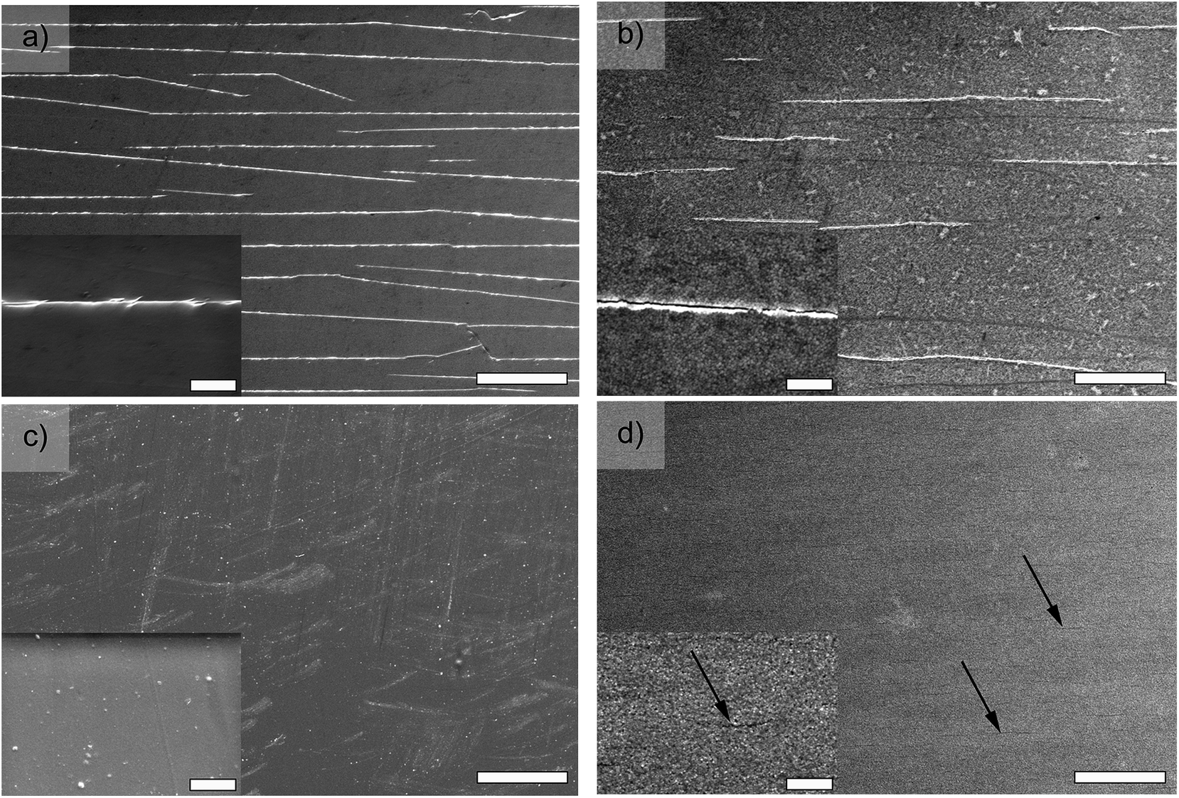 | ||
| Fig. 4 Low-magnification (main) and high-magnification (inset) SEM images of: (a) PET/M-In2O3, (b) PET/M-In2O3/ZnO/CH3NH3PbI3, (c) PET/HC-PEDOT, and (d) PET/HC-PEDOT/SC-PEDOT/CH3NH3PbI3 films after 2000 bending cycles. The scale bars in the main and inset images are 50 μm and 5 μm, respectively. The arrows in (d) show the location of small cracks in the perovskite layer. | ||
Finally, in order to confirm that these results are consistent across both M-In2O3 and ITO electrodes, we repeated the work on commercially available ITO/PET substrates. The sheet resistance (ca. 40 Ω □−1) was found to be higher than that of the M-In2O3 electrodes, with a correspondingly higher optical transmittance (Fig. S7†). The device performance (Fig. S7†) was found to be similar to that reported previously,2 and the fatigue resistance (Fig. S8†) was very similar to that of the M-In2O3 electrodes (Fig. 3). Both ITO and M-In2O3 devices failed via the same sudden cracking of the transparent conductive oxide (Fig. S9†), with the sheet resistance of the ITO electrode increasing to 1.4 × 10³ Ω □−1 after 2200 bending cycles.
Conclusions
Through the use of a HC-PEDOT transparent electrode, we have successfully fabricated a flexible perovskite solar cell containing no inorganic metal-oxide layers for the first time. The devices show power conversion efficiencies as high as 7.6% and very low hysteresis. The fatigue resistance of these devices, as well as those based on an In2O3 transparent electrode, was determined by repeatedly bending them around a cylindrical object of 4 mm radius for 2000 bending cycles. Our observations indicate that it is the metal-oxide transparent electrode that ultimately limits the mechanical flexibility of these devices, and the use of the HC-PEDOT electrode circumvents this limit. The fatigue resistance of the perovskite solar cells was then compared to that of polymer-based devices, and it was found that the performance of the perovskite devices decreases more rapidly due to the formation of small cracks in the perovskite layer. Our results suggest that although the perovskite layer is incompatible with repeated bending at a low radius of curvature (as might be encountered in textile-integrated photovoltaics), it is more than robust enough for the more moderate conditions typically encountered in R2R manufacturing. This study outlines important limitations on the flexibility of conventional perovskite solar cells, which have important implications for their manufacture and eventual commercial application.Experimental
HC-PEDOT/SC-PEDOT/CH3NH3PbI3 device fabrication
The HC-PEDOT solution (Clevios PH1000) was mixed with 5% (v/v) dimethyl sulfoxide and 0.5% (v/v) Zonyl F-300 fluorosurfactant. After filtration through a 0.45 μm polyvinylidene difluoride (PVDF) syringe filter, 300 μL of the solution was dispensed onto a 2.54 cm × 2.54 cm pre-cleaned PET substrate. The sample was spin-coated at 1000 rpm for 1 min and 2000 rpm for 1 min. A highly porous chuck was used for all spin-coating steps. The samples were thermally annealed at 120 °C for 30 min.35 A thin strip of silver paint was used to deposit a mechanically-robust electrical contact to the HC-PEDOT electrode. A SC-PEDOT solution (Clevios P VP AI 4083) was filtered through a 0.45 μm filter, and 300 μL spin-coated (1200 rpm for 30 s followed by 3000 rpm for 10 s) onto the substrate.41 The samples were again annealed at 120 °C for 5–10 min, after which they were immediately transferred into a glovebox (<0.1 ppm O2 and H2O). A 460 mg mL−1 PbI2 solution was prepared in dry N,N-dimethylformamide and kept at 100 °C. Samples were again thermally annealed at 100 °C for 5–10 min, immediately after which the PbI2 solution (100 μL) was deposited by spin-coating (3000 rpm for 20–25 s, using a dynamic dispensing step). The PbI2 layer was allowed to dry for 2 h, after which the samples were brought out of the glovebox, immersed in a 10 mg mL−1 CH3NH3I solution in dry isopropanol for 60 s, and then spin-dried at 2000 rpm for 10 s. They were immediately transferred back into the glovebox. PC61BM was deposited by spin-coating (1000 rpm for 45 s, followed by 4000 rpm for 10 s) from 100 μL of a 20 mg mL−1 PC61BM in chlorobenzene solution, which was pre-stirred for at least 2 h. Al counter-electrodes were deposited by thermal evaporation at a base pressure of 2 × 10⁻⁶ mbar at a rate of 1 Å s−1 for the first ∼40 nm and at a rate of 3 Å s−1 for another ∼145 nm.Device characterization
Device illumination was provided by a 450 W Class AAA solar simulator equipped with an AM 1.5G filter (Sol3A, Oriel Instruments). The light intensity was set to 100 mA cm−2 using a standard silicon reference cell (91150V, Oriel Instruments). J–V curves were obtained with a Keithley 2400 source-measure unit. The area of the device under illumination was fixed at 0.0708 cm2 using a non-reflective metal mask. The pre-sweep delay time was 1 s, the dwell time at each voltage step was 30 ms, and 85 data points were measured between −0.4 and 2.0 V. All bending tests were done in a glovebox environment (<0.1 ppm O2 and H2O), and care was taken to ensure that the entire device area was uniformly bent around the cylindrical object. Before remeasuring the J–V curves, the devices were bent gently in the converse direction to minimize any curvature caused by bending.Acknowledgements
The Natural Sciences and Engineering Research Council of Canada (NSERC) and the University of Saskatchewan are acknowledged for financial support. T.L.K. is a Canada Research Chair in Photovoltaics. The research was undertaken, in part, thanks to funding from the Canada Research Chair program. K.P. thanks the College of Arts & Science at the University of Saskatchewan for a Graduate Catalyst Award.References
- M. A. Green, K. Emery, Y. Hishikawa, W. Warta and E. D. Dunlop, Prog. Photovolt. Res. Appl., 2014, 22, 701–710 CrossRef.
- D. Liu and T. L. Kelly, Nat. Photonics, 2014, 8, 133–138 CrossRef CAS.
- H. Zhou, Q. Chen, G. Li, S. Luo, T. B. Song, H. S. Duan, Z. Hong, J. You, Y. Liu and Y. Yang, Science, 2014, 345, 542–546 CrossRef CAS PubMed.
- N. J. Jeon, J. H. Noh, Y. C. Kim, W. S. Yang, S. Ryu and S. I. Seok, Nat. Mater., 2014, 13, 897–903 CrossRef CAS PubMed.
- J. W. Lee, D. J. Seol, A. N. Cho and N. G. Park, Adv. Mater., 2014, 26, 4991–4998 CrossRef CAS PubMed.
- R. F. Service, Science, 2014, 344, 458 CrossRef PubMed.
- Z. Wei, K. Yan, H. Chen, Y. Yi, T. Zhang, X. Long, J. Li, L. Zhang, J. Wang and S. Yang, Energy Environ. Sci., 2014, 7, 3326–3333 CAS.
- J. Liu, Y. Wu, C. Qin, X. Yang, T. Yasuda, A. Islam, K. Zhang, W. Peng, W. Chen and L. Han, Energy Environ. Sci., 2014, 7, 2963–2967 CAS.
- F. Hao, C. C. Stoumpos, D. H. Cao, R. P. H. Chang and M. G. Kanatzidis, Nat. Photonics, 2014, 8, 489–494 CrossRef CAS.
- M. D. McGehee, Nat. Mater., 2014, 13, 845–846 CrossRef CAS PubMed.
- M. Grätzel, Nat. Mater., 2014, 13, 838–842 CrossRef PubMed.
- F. Zuo, S. T. Williams, P.-W. Liang, C.-C. Chueh, C.-Y. Liao and A. K. Y. Jen, Adv. Mater., 2014, 26, 6454–6460 CrossRef CAS PubMed.
- P. Docampo, J. M. Ball, M. Darwich, G. E. Eperon and H. J. Snaith, Nat. Commun., 2013, 4, 2761 Search PubMed.
- C. Roldán-Carmona, O. Malinkiewicz, A. Soriano, G. Mínguez Espallargas, A. Garcia, P. Reinecke, T. Kroyer, M. I. Dar, M. K. Nazeeruddin and H. J. Bolink, Energy Environ. Sci., 2014, 7, 994–997 Search PubMed.
- Editorial, Nat. Nanotechnol., 2014, 9, 657 CrossRef PubMed.
- P. Qin, S. Tanaka, S. Ito, N. Tetreault, K. Manabe, H. Nishino, M. K. Nazeeruddin and M. Gratzel, Nat. Commun., 2014, 5, 3834 CAS.
- K. Wojciechowski, M. Saliba, T. Leijtens, A. Abate and H. J. Snaith, Energy Environ. Sci., 2014, 7, 1142–1147 CAS.
- S. Kazim, M. K. Nazeeruddin, M. Gratzel and S. Ahmad, Angew. Chem., Int. Ed., 2014, 53, 2812–2824 CrossRef CAS PubMed.
- Q. Wang, Y. Shao, Q. Dong, Z. Xiao, Y. Yuan and J. Huang, Energy Environ. Sci., 2014, 7, 2359–2365 CAS.
- L. Qiu, J. Deng, X. Lu, Z. Yang and H. Peng, Angew. Chem., Int. Ed., 2014, 53, 10425–10428 CrossRef CAS PubMed.
- B.-J. Kim, d. H. Kim, Y.-Y. Lee, H.-W. Shin, G. S. Han, J. S. Hong, K. Mahmood, T. Ahn, Y.-C. Joo, K. S. Hong, N.-G. Park, S. Lee and H. S. Jung, Energy Environ. Sci., 2015 10.1039/c4ee02441a.
- J. Feng, APL Mater., 2014, 2, 081801 CrossRef PubMed.
- O. Inganas, Nat. Photonics, 2011, 5, 201–202 CrossRef.
- S. Pang, Y. Hernandez, X. Feng and K. Mullen, Adv. Mater., 2011, 23, 2779–2795 CrossRef CAS PubMed.
- J. Liu, D. B. Buchholz, R. P. Chang, A. Facchetti and T. J. Marks, Adv. Mater., 2010, 22, 2333–2337 CrossRef CAS PubMed.
- Y. Li, D.-K. Lee, J. Y. Kim, B. Kim, N.-G. Park, K. Kim, J.-H. Shin, I.-S. Choi and M. J. Ko, Energy Environ. Sci., 2012, 5, 8950–8957 CAS.
- K. Ellmer, Nat. Photonics, 2012, 6, 809–817 CrossRef CAS.
- D. S. Hecht, L. Hu and G. Irvin, Adv. Mater., 2011, 23, 1482–1513 CrossRef CAS PubMed.
- S. Soltanian, R. Rahmanian, B. Gholamkhass, N. M. Kiasari, F. Ko and P. Servati, Adv. Energy Mater., 2013, 3, 1332–1337 CrossRef CAS.
- F. Bonaccorso, Z. Sun, T. Hasan and A. C. Ferrari, Nat. Photonics, 2010, 4, 611–622 CrossRef CAS.
- S. Seo, M. Min, S. M. Lee and H. Lee, Nat. Commun., 2013, 4, 1920 CrossRef PubMed.
- D. Chen, H. Zhang, Y. Liu and J. Li, Energy Environ. Sci., 2013, 6, 1362–1387 CAS.
- S.-I. Na, S.-S. Kim, J. Jo and D.-Y. Kim, Adv. Mater., 2008, 20, 4061–4067 CrossRef CAS.
- Y. H. Kim, C. Sachse, M. L. Machala, C. May, L. Müller-Meskamp and K. Leo, Adv. Funct. Mater., 2011, 21, 1076–1081 CrossRef CAS.
- M. Kaltenbrunner, M. S. White, E. D. Glowacki, T. Sekitani, T. Someya, N. S. Sariciftci and S. Bauer, Nat. Commun., 2012, 3, 770 CrossRef PubMed.
- D. Alemu, H.-Y. Wei, K.-C. Ho and C.-W. Chu, Energy Environ. Sci., 2012, 5, 9662–9671 CAS.
- Y. Xia, K. Sun and J. Ouyang, Adv. Mater., 2012, 24, 2436–2440 CrossRef CAS PubMed.
- C.-Y. Chang, L. Zuo, H.-L. Yip, C.-Z. Li, Y. Li, C.-S. Hsu, Y.-J. Cheng, H. Chen and A. K. Y. Jen, Adv. Energy Mater., 2014, 4, 1301645 Search PubMed.
- V. W. Bergmann, S. A. L. Weber, F. Javier Ramos, M. K. Nazeeruddin, M. Grätzel, D. Li, A. L. Domanski, I. Lieberwirth, S. Ahmad and R. Berger, Nat. Commun., 2014, 5, 5001 CrossRef PubMed.
- J. Seo, S. Park, Y. Chan Kim, N. J. Jeon, J. H. Noh, S. C. Yoon and S. I. Seok, Energy Environ. Sci., 2014, 7, 2642–2646 CAS.
- O. Malinkiewicz, A. Yella, Y. H. Lee, G. M. Espallargas, M. Graetzel, M. K. Nazeeruddin and H. J. Bolink, Nat. Photonics, 2014, 8, 128–132 CrossRef CAS.
- D. Liu, M. K. Gangishetty and T. L. Kelly, J. Mater. Chem. A, 2014, 2, 19873–19881 CAS.
- H. J. Snaith, A. Abate, J. M. Ball, G. E. Eperon, T. Leijtens, N. K. Noel, S. D. Stranks, J. T.-W. Wang, K. Wojciechowski and W. Zhang, J. Phys. Chem. Lett., 2014, 5, 1511–1515 CrossRef CAS.
- R. S. Sanchez, V. Gonzalez-Pedro, J.-W. Lee, N.-G. Park, Y. S. Kang, I. Mora-Sero and J. Bisquert, J. Phys. Chem. Lett., 2014, 5, 2357–2363 CrossRef CAS.
- E. L. Unger, E. T. Hoke, C. D. Bailie, W. H. Nguyen, A. R. Bowring, T. Heumuller, M. G. Christoforo and M. D. McGehee, Energy Environ. Sci., 2014, 7, 3690–3698 CAS.
- E. Zimmermann, P. Ehrenreich, T. Pfadler, J. A. Dorman, J. Weickert and L. Schmidt-Mende, Nat. Photonics, 2014, 8, 669–672 CrossRef CAS.
- Z. Xiao, C. Bi, Y. Shao, Q. Dong, Q. Wang, Y. Yuan, C. Wang, Y. Gao and J. Huang, Energy Environ. Sci., 2014, 7, 2619–2623 CAS.
- Z. Xiao, Q. Dong, C. Bi, Y. Shao, Y. Yuan and J. Huang, Adv. Mater., 2014, 26, 6503–6509 CrossRef CAS PubMed.
- W. Chen, W. Yongzhen, J. Liu, C. Qin, X. Yang, A. Islam, Y.-B. Cheng and L. Han, Energy Environ. Sci., 2015 10.1039/c4ee02833c.
- J. H. Kim, P.-W. Liang, S. T. Williams, N. Cho, C.-C. Chueh, M. S. Glaz, D. S. Ginger and A. K. Y. Jen, Adv. Mater., 2015, 27, 695–701 CrossRef CAS PubMed.
- P.-W. Liang, C.-C. Chueh, X.-K. Xin, F. Zuo, S. T. Williams, C.-Y. Liao and A. K. Y. Jen, Adv. Energy Mater., 2015, 5, 1400960 Search PubMed.
- K. Wojciechowski, S. D. Stranks, A. Abate, G. Sadoughi, A. Sadhanala, N. Kopidakis, G. Rumbles, C.-Z. Li, R. H. Friend, A. K. Y. Jen and H. J. Snaith, ACS Nano, 2014, 8, 12701–12709 CrossRef CAS PubMed.
- Y. Shao, Z. Xiao, C. Bi, Y. Yuan and J. Huang, Nat. Commun., 2014, 5, 5784 CrossRef PubMed.
Footnote |
| † Electronic supplementary information (ESI) available: Materials, device fabrication and characterization procedures, absorption spectra, pXRD patterns, J–V curves, results of fatigue resistance and bending radius tests, SEM images, organic solar cell performance data, statistical test results, data for devices on ITO electrodes. See DOI: 10.1039/c5ta00084j |
| This journal is © The Royal Society of Chemistry 2015 |