
Vertically aligned nanocomposite La0.8Sr0.2CoO3/(La0.5Sr0.5)2CoO4 cathodes – electronic structure, surface chemistry and oxygen reduction kinetics†
Wen
Ma
a,
Jae Jin
Kim
b,
Nikolai
Tsvetkov
a,
Takeshi
Daio
c,
Yener
Kuru
ab,
Zhuhua
Cai
a,
Yan
Chen
a,
Kazunari
Sasaki
c,
Harry L.
Tuller
b and
Bilge
Yildiz
*a
aLaboratory for Electrochemical Interfaces, Department of Nuclear Science and Engineering, Massachusetts Institute of Technology, 77 Massachusetts Avenue, Cambridge, MA 02139, USA. E-mail: byildiz@mit.edu
bDepartment of Materials Science and Engineering, Massachusetts Institute of Technology, 77 Massachusetts Avenue, Cambridge, MA 02139, USA
cDepartment of Mechanical Engineering, Kyushu University, Fukuoka-shi, 819-0395 Fukuoka, Japan
First published on 24th October 2014
Abstract
The hetero-interfaces between the perovskite (La1−xSrx)CoO3 (LSC113) and the Ruddlesden-Popper (La1−xSrx)2CoO4 (LSC214) phases have recently been reported to exhibit fast oxygen exchange kinetics. Vertically aligned nanocomposite (VAN) structures offer the potential for embedding a high density of such special interfaces in the cathode of a solid oxide fuel cell in a controllable and optimized manner. In this work, VAN thin films with hetero-epitaxial interfaces between LSC113 and LSC214 were prepared by pulsed laser deposition. In situ scanning tunneling spectroscopy established that the LSC214 domains in the VAN structure became electronically activated, by charge transfer across interfaces with adjacent LSC113 domains above 250 °C in 10−3 mbar of oxygen gas. Atomic force microscopy and X-ray photoelectron spectroscopy analysis revealed that interfacing LSC214 with LSC113 also provides for a more stable cation chemistry at the surface of LSC214 within the VAN structure, as compared to single phase LSC214 films. Oxygen reduction kinetics on the VAN cathode was found to exhibit approximately a 10-fold enhancement compared to either single phase LSC113 and LSC214 in the temperature range of 320–400 °C. The higher reactivity of the VAN surface to the oxygen reduction reaction is attributed to enhanced electron availability for charge transfer and the suppression of detrimental cation segregation. The instability of the LSC113/214 hetero-structure surface chemistry at temperatures above 400 °C, however, was found to lead to degraded ORR kinetics. Thus, while VAN structures hold great promise for offering highly ORR reactive electrodes, efforts towards the identification of more stable hetero-structure compositions for high temperature functionality are warranted.
1. Introduction
Solid oxide fuel cells (SOFCs) have high energy conversion efficiencies and lower emissions than combustion systems by virtue of their ability to directly convert the chemical energy stored in fuels into electrical energy at elevated temperatures.1 To render them economically feasible, functionality at intermediate temperatures (500–700 °C), and at even lower temperatures (350–500 °C) for microdevices, is desirable, thereby lowering the cost and increasing the lifetime of SOFC systems.2–8 At these reduced temperatures, however, the performance of the cathode becomes a challenge, due to the sluggish kinetics of the oxygen reduction reaction on traditionally used cathode materials. The cathode effectively catalyzes the oxygen reduction by providing available sites9,10 for oxygen adsorption and by transferring electrons from the solid to the adsorbing oxygen in a facile manner.4,11,12There has been several recent reports showing that interfaces between the perovskite (La1−xSrx)CoO3 (LSC113) and the Ruddlesden-Popper (La1−xSrx)2CoO4 (LSC214) phases in the LSC113/214 hetero-structure significantly facilitate oxygen reduction kinetics.13–17 Sase et al.14,15 showed that the oxygen exchange kinetics near these dissimilar interfaces is increased by three to four orders of magnitude with respect to single phase LSC113 or LSC214 at 500 °C. Such an astonishing improvement of oxygen exchange kinetics was also confirmed by electrochemical measurements at 550 °C and 600 °C.16,17 In order to go beyond this isolated example and design active and stable hetero-interfaces for accelerating ORR in a controllable way on oxide surfaces, a microscopic level understanding of the mechanisms behind such an unusual enhancement is needed. For this purpose, we recently reported on the electronic structure at the surface of LSC113/214 hetero-structures, in the form of multilayers, by performing in situ scanning tunneling spectroscopy (STS) as a function of temperature and in oxygen gas.18 The STS measurements were assisted by grazing incidence focused ion beam milling to expose the buried interfaces and layers with nm-scale resolution. Tunneling spectroscopy results revealed that the p-type LSC214 loses its energy gap at the surface and becomes enriched in electrons when put in contact with LSC113 at elevated temperatures. Considerably more electrons become available to reduce the oxygen at the LSC214 surface. That, combined with the preferential anisotropic oxygen incorporation into LSC214 (100) surfaces,19 is expected to accelerate ORR kinetics at the LSC113/214 hetero-structures (Fig. 1a).20 This finding allowed us to propose “electronically coupled oxide hetero-structures” as a new type of high-performance cathode for SOFCs.
 | ||
| Fig. 1 (a) Schematic model of “electronically coupled oxide hetero-structures” made of LSC113 and LSC214. At high temperature, more oxygen vacancies and free electrons are created in the LSC113 phase. The excess electrons are injected into LSC214 phase from LSC113, facilitating the oxygen reduction reaction at the LSC214 surface. Faster ORR kinetics are expected at LSC113/214 vertically aligned nanocomposite hetero-structures given the high density of interfaces. (Note the alignment between LSC113/LSC214 does not reflect the real geometry.) (b) Schematic checker-board illustration of a vertically aligned nanocomposite (VAN) made of LSC113 and LSC214 on a substrate. | ||
Inspired by this model,18 the vertically aligned nanocomposite (VAN) of LSC113/214, which benefits from the electronic activation phenomena, while maximizing the desirable active interfacial area exposed to the gas phase, is studied in this work as a new cathode structure (Fig. 1b). This serves as a more controllable alternative to the random decoration of surfaces of a phase with nano-particles of a second phase or to making a randomly mixed composite cathode.16,17 Vertical nanocomposite hetero-epitaxial films are of interest for various functional device applications. Fig. 1b illustrates an idealized model of such nanocomposites in which the two phases alternate in an ordered, checker-board fashion. VAN structures have been demonstrated in a number of material systems, in order to examine the tunability of electrical conductivity,21 dielectric loss22,23 and low-field magnetoresistance23 mediated by the strain at the hetero-epitaxial interfaces. VAN oxide thin films have also stimulated interest in the field of SOFC research. Yoon et al.24 demonstrated one to two orders of magnitude decrease of area-specific resistance of the cathode by forming a Ce0.9Gd0.1O1.95/La0.5Sr0.5CoO3 VAN interlayer between the cathode and the electrolyte, and this interlayer effectively increased the cathode/electrolyte interfacial contact area. The oxide ion conductivity of (Ce0.9Gd0.1O1.95)/(Zr0.92Y0.08O1.96) VAN electrolyte has also been reported to be enhanced by two times compared with YSZ or GDC thin films.25 Vertically aligned nanocomposites made of different cathode materials have not been previously studied however and are examined in detail in this study of the LSC113/214 system. Both LSC113 and LSC214 grow epitaxially on common substrates, such as SrTiO3 (STO) and yttria stabilized zirconia (YSZ) with a gadolinium doped ceria (GDC) buffer layer.26–28 Given that both LSC113 and LSC214 also exhibit similar growth kinetics and that it is possible for them to phase separate in a thermodynamically stable state,14,17,18 the LSC113/214 composite system offers the possibility to form high quality VAN structures.
The unique requirements needed to successfully grow and characterize the LSC113/214 VAN structures under in situ conditions are described in the Experimental section below. In particular, it is worth noting that the proper synthesis conditions to form columnar growth of LSC113 and LSC214 in a phase-separated form in the VAN structure were found to reside only in a narrow temperature window, oxygen partial pressure and deposition rate during the pulsed laser deposition (See Experimental methods for details). Nano-probe Auger electron spectroscopy and in situ scanning tunneling microscopy were used to characterize the chemical, structural and electronic properties of the nanocomposite LSC113/214 film with high spatial resolution. Moreover, to access the properties of these VAN structures under conditions close to the working environment of an SOFC, in situ scanning tunneling spectroscopy,18,26,29,30 with ability to operate at elevated temperatures and in oxygen gas, served to capture novel changes in the electronic structure of the VAN surface as a function of temperature.
In this work, we demonstrate the successful formation of vertically aligned nanocomposites of LSC113/214. LSC113 and LSC214 phases form (00l) orientated columnar grains with lateral dimensions in the range of 100–500 nm. Two key features, described in the Results, are the disappearance of the 0.7–1 eV energy gap at the surface of LSC214 when it is in the VAN structure at and above 250 °C in oxygen gas, and the improved stability of the cation composition at the surface of LSC214 when it is part of the VAN hetero-structure. We believe these two factors give rise to enhanced ORR kinetics, by about one order of magnitude, for LSC113/214 VAN thin films at, or below, 400 °C, as shown by our electrochemical impedance measurements. Challenges related to long-term stability of these particular LSC113/214 compositions used in the VAN structure at temperatures above 400 °C are also discussed.
2. Experimental methods
The (La0.8Sr0.2)CoO3/(La0.5Sr0.5)2CoO4 nanocomposite film was prepared by pulsed laser deposition from a composite target onto SrTiO3 (001) and yttria stabilized zirconia (YSZ) (001) single crystal substrates (purchased from MTI Corp). In this study, La0.8Sr0.2CoO3 and (La0.5Sr0.5)2CoO4 were chosen because these compositions were demonstrated by Crumlin et al.16 and Sase et al.14 to exhibit enhanced electrochemical performance with hetero-structures, albeit composed of random surface patches of LSC214 on LSC113. For the composite target preparation, first, single-phase (La0.8Sr0.2)CoO3 and (La0.5Sr0.5)2CoO4 powders were synthesized by the Pechini gel-type method31 utilizing La(NO3)3·6H2O, Sr(NO3)2, Co(NO3)2·6H2O, ethylene glycol and anhydrous citric acid as the starting materials. Aqueous solutions of the metal nitrates were mixed in the respective stoichiometric ratio by stirring, followed by addition of ethylene glycol and citric acid to form a metal–organic complex. The resultant mixtures were heated at 90 °C until a dry gel formed. After drying at 110 °C for 12 h, the as-obtained powder was prefired at 500 °C for 2 h and then fully calcined at 950 °C for 5 h. The phase composition of the powders was examined by X-ray diffraction (CuKα, 45 kV and 40 mA, PANalytical X'Pert Pro Multipurpose Diffractometer, Almelo, Netherlands) at room temperature in air. In order to fabricate the composite oxide target made of (La0.8Sr0.2)CoO3 and (La0.5Sr0.5)2CoO4, the two powders were thoroughly mixed in a 3![[thin space (1/6-em)]](https://www.rsc.org/images/entities/char_2009.gif) :2 molar ratio. After uniaxially pressing under ∼100 MPa for 90 seconds, the target was sintered at 1300 °C for 10 hours in air. The LSC113 and LSC214 phases remained phase separated even following sintering under these conditions as confirmed by nanoprobe Auger Electron Spectrometry measurements used to quantify the chemical composition in each phase (Table S1†). A KrF excimer laser with wavelength of 248 nm under energy constant mode (300 mJ) and pulse frequency of 2 Hz was used during deposition. Since LSC is reactive with YSZ, a 10% gadolinium doped ceria Ce0.9Gd0.1O1.95 (GDC) buffer layer was deposited on the YSZ (001) substrate at 680 °C under 10 mTorr oxygen partial pressure by pulsed laser deposition in the same chamber preceding the deposition of the LSC113/214 VAN films. The deposition conditions for the VAN film were 760 °C substrate temperature and 100 mTorr oxygen partial pressure. Following growth, the films were cooled down to room temperature in 10 Torr oxygen pressure to ensure oxidation of the films. The resulting LSC113, LSC214 and LSC113/214 VAN dense films of ∼200 nm thickness were deposed either on YSZ (001) substrates coated with ∼100 nm thick GDC buffer layers, or directly onto STO (001) substrates.
:2 molar ratio. After uniaxially pressing under ∼100 MPa for 90 seconds, the target was sintered at 1300 °C for 10 hours in air. The LSC113 and LSC214 phases remained phase separated even following sintering under these conditions as confirmed by nanoprobe Auger Electron Spectrometry measurements used to quantify the chemical composition in each phase (Table S1†). A KrF excimer laser with wavelength of 248 nm under energy constant mode (300 mJ) and pulse frequency of 2 Hz was used during deposition. Since LSC is reactive with YSZ, a 10% gadolinium doped ceria Ce0.9Gd0.1O1.95 (GDC) buffer layer was deposited on the YSZ (001) substrate at 680 °C under 10 mTorr oxygen partial pressure by pulsed laser deposition in the same chamber preceding the deposition of the LSC113/214 VAN films. The deposition conditions for the VAN film were 760 °C substrate temperature and 100 mTorr oxygen partial pressure. Following growth, the films were cooled down to room temperature in 10 Torr oxygen pressure to ensure oxidation of the films. The resulting LSC113, LSC214 and LSC113/214 VAN dense films of ∼200 nm thickness were deposed either on YSZ (001) substrates coated with ∼100 nm thick GDC buffer layers, or directly onto STO (001) substrates.
The surface cation chemistry was quantified with nm-scale spatial resolution by Scanning Nano-probe Auger Electron Spectrometry (AES) (Physical Electronics Model 700). Specifically, Co distribution was mapped to identify the phases in the VAN, and the Sr fractions in the LSC113 and LSC214 grains in the VAN were quantified and found to be similar to those in the single phase LSC113 and LSC214 films (see ESI, Table S1†). The energy and current of the incident electrons were 10 keV and 10 nA, respectively. Smoothing and differentiation of the Auger electron spectra were performed using the Savitsky-Golay algorithm. Quantification of the Auger electron differential spectra was carried out using the peak-to-peak intensities of the tight scans of the La MNN, Sr LMM, and Co LMM Auger electron emissions. The sampling depths of these Auger electrons are ∼4 nm for La MNN, ∼8.5 nm for Sr LMM and ∼4.6 nm for Co LMM.32
Cross-sectional Scanning Electron Microscopy (SEM-FEI Helios Nanolab system) was used to identify the columnar microstructure of the VAN film. The film was cut vertically with respect to the sample surface by focused Ga+ ion-beam (FIB). In order to protect the surface features during ion milling, a ∼1 μm thick Pt protective cap was deposited on top by electron beam. The Ga+ beam current and acceleration voltage were 6.5 nA and 30 kV, respectively. The exposed interface was then cleaned by decreasing the beam current to, e.g. 2.8 nA, 0.28 nA and 93 pA. The surface was coated with gold by ion sputtering to minimize charging during SEM. Then the exposed vertical surface was subject to SEM imaging with the electron beam inclined 38° from the film surface.
Scanning Transmission Electron Microscopy (STEM) images were acquired using a JEOL ARM-200F (with a resolution of 0.07 nm), equipped with a Cold FEG and a CEOS STEM Probe corrector. The acceleration voltage of the STEM was 200 kV. Cross sectional layer STEM sample of ca. 100 nm thickness was fabricated by FIB milling. Prior to STEM examination, as a final stage of the sample preparation, Ar+ ion milling at 990 V was used to remove potential damage during FIB sectioning. Electron energy loss spectroscopy (EELS) and energy dispersive X-ray spectroscopy (EDX) analysis were performed with an Enfinium Spectrometer (Gatan, U.S.) equipped with a JEM-ARM200F. The EELS and EDX signals were simultaneously acquired by a Digital Micrograph (Gatan, U.S.) detector.
Angle resolved X-ray photoelectron spectroscopy (XPS) measurement, using a PHI Versaprobe II system, were performed to identify the depth resolved surface chemistry. The photoelectron spectra at La 4d, Sr 3d, La 3d and Co 2p emissions were used to calculate the surface cation composition. These spectra were measured at different emission angles, 0°, 45° and 70°, between the surface normal and the detector position for varying the depth resolution from bulk to the surface. For the excitation energy of 1486.6 eV, the sampling depths of photoelectrons at 0° emission angle are ∼6 nm for Sr 3d and La 4d, and ∼3.4 nm for La 3d and Co 2p.32 CasaXPS 2.3.16 software was used for peak analysis and quantification.
The crystallography of the as-deposited samples was confirmed by high-resolution X-ray diffraction measurements. For identifying the crystal structure, the 2θ − ω scans were measured by a high resolution four circle Bruker D8 Discover diffractometer, equipped with a Göbel mirror, 4-bounce Ge (022) channel-cut monochromator, Eulerian cradle, and a scintillation counter, using Cu Kα1 radiation.
Scanning tunneling microscopy and spectroscopy (STM/STS) measurements were performed by a modified variable-temperature scanning tunneling microscope (VT-STM) (Omicron GmbH, Germany) with high spatial resolution from room temperature to 300 °C and in oxygen environment (10−3 mbar in this work). A retractable oxygen doser placed near the STM stage in the chamber was used to directly expose the sample to oxygen during the experiments. STM images were acquired in constant-current mode using Pt/Ir tips prepared by chemical etching. A tip bias voltage of 2–2.5 V and feedback tunneling current of 50–500 pA were used during measurements. For surface cleaning and in situ measurements, samples were heated in oxygen using a pyrolytic boron nitride (PBN) heater. To obtain high quality images and tunneling spectra, the sample was cleaned prior to the STM/STS measurements by first sputtering the surface by low energy Ar+ (0.5 keV) for 100 seconds, followed by heating in high purity oxygen at 350 °C and 2 × 10⁻⁵ mbar pressure for 1 hour. This served to remove the water and carbon-related adsorbates from the surface due to air-exposure after film growth.
Surface morphology of LSC113, LSC214 and LSC113/214 VAN cathode thin films were measured by atomic force microscopy (AFM) (Veeco Metrology Nanoscope IV Scanned Probe Microscope Controller with Dimension 3100 SPM). As-prepared surface was monitored after the samples were subsequently annealed at 370 °C and 620 °C in air, in the chamber used for the electrochemical tests in this work.
Electrochemical impedance spectroscopy (EIS) measurements were performed on asymmetrical cell structures with the LSC113, LSC214 and LSC113/214 VAN cathode dense film structures grown on YSZ (001) single crystals (10 × 10 × 0.5 mm3, MTI Corporation, Richmond, CA) with Ce0.9Gd0.1O1.95 (GDC) buffer layers. Gold mesh current collectors (20 × 20 μm2 of open area in every 40 × 40 μm2 repeat unit in the total 7.3 × 7.3 mm2 current collector area) were deposited on the LSC thin films utilizing photolithography and RF sputtering. Porous Ag counter electrodes were applied as the counter electrode. Platinum wire leads were connected to the current collector and the counter electrode with the aid of the lab-designed mechanical clip made of Pt–Ir 20% alloy wire (4 N purity, ESPI metals, Ashland OR). EIS measurements were performed in the frequency range of 1 mHz to 1 MHz with AC amplitude of 20 mV and zero DC bias at temperatures between 320 °C and 620 °C, using the ModuLab system (Solartron Analytical) in conjunction with the FRA 1 MHz (2055A) Frequency Response Analyzer module or the Solartron 1250 impedance analyzer operated in combination with a Solartron 1286 potentiostat. ZView software (Scribner Associates, USA) was used to fit the data and construct equivalent circuits to analyze the impedance data.
3. Results
3.1 Structure and growth mechanism of the LSC113/214 VAN films
The cross-sectional SEM image of the LSC113/214 films on STO (001) and YSZ (001) substrates indicated a columnar structure, as shown in Fig. 2a. For the LSC113/214 VAN films grown on the YSZ (001) substrate, the GDC buffer layer was uniform, while a columnar contrast in the VAN layer is evident. The different contrast in the films stems from the different electronic conductivities of the LSC113 and LSC214 domains. The thickness of the film, after correcting for tilting, is ∼160 nm, while the average width of the columns is ∼300 nm. The near-vertical separation of the LSC113 and LSC214 phases can also be observed in the high resolution STEM image of the atomic structure in Fig. 2b. Further detailed STEM-EDX analysis shows no increase or decrease of Sr content across the interface region (Fig. 2c). The Sr/(Sr + La) ratios are 0.32 in LSC113 and 0.45 in LSC214 columns (Table S2†), results consistent with the AES analysis (Table S1†).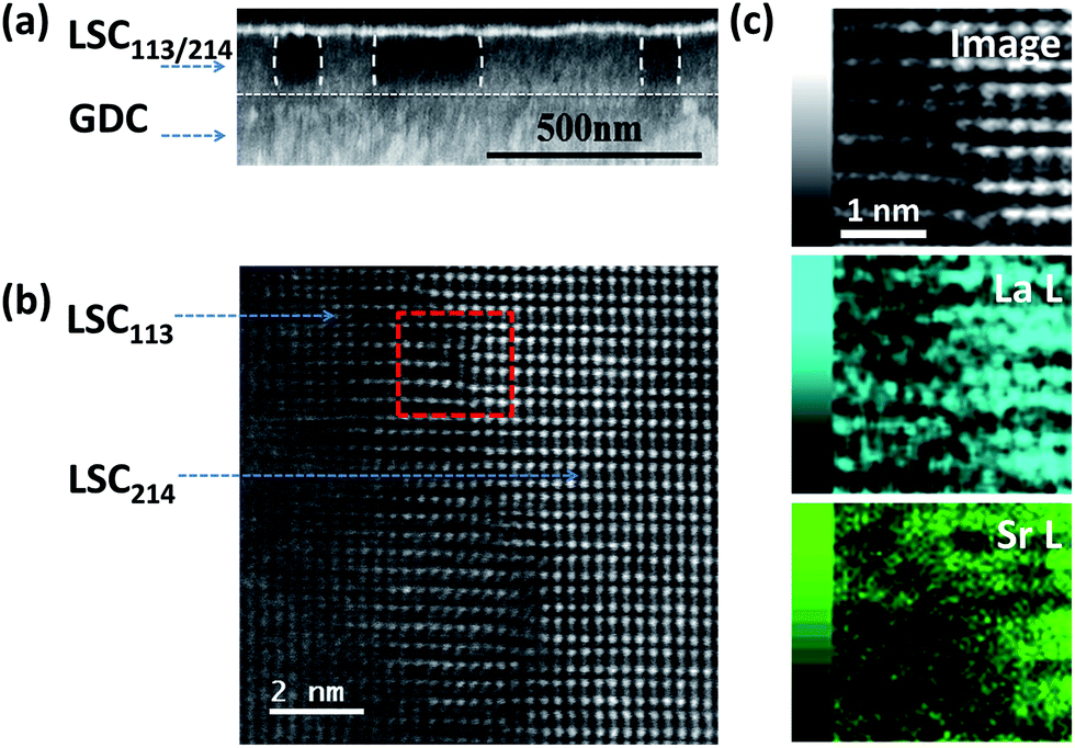 | ||
| Fig. 2 (a) Cross-sectional SEM image of the LSC113/214 VAN film on the YSZ (001) substrate with a GDC interlayer. (b) STEM image near the interface of LSC113 and LSC214 columns. (c) Zoomed-in STEM image of the region marked by the red dashed square in (b) and STEM-EDX mapping of La L and Sr L signals in that region. | ||
Phase identification was also achieved by mapping the Co LMM Auger signal intensity. Fig. 3a shows the concentration distribution of Co cations on the sample surface mapped spatially by the Auger nano-probe. The intensity of the Co peak in the Auger spectrum is an indication of the Co concentration in the sample. The number density (atomic concentration) of Co is 1.8 × 1028 m−3 and 5.6 × 1027 m−3 for stoichiometric LSC113 and LSC214, respectively. The bright regions are the Co rich phase assigned to the LSC113 domains, while the dark regions are assigned to the LSC214 domains. The image contrast, as recorded by SEM (Fig. 3b), matches the Co distribution shown in Fig. 3a. The contrast on the SEM image originates from the differences in the conductivity of these two phases (LSC214 is more insulating than LSC113 (ref. 33 and 34)). Image contrast and the grain (or domain) size on the order of hundreds of nm are also consistent with the cross-sectional SEM image in Fig. 2.
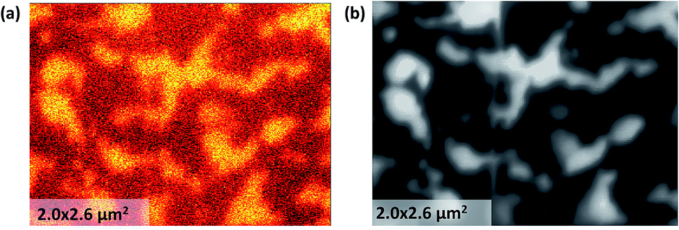 | ||
| Fig. 3 (a) Auger spectrum mapping of Co cation concentration at the surface of the LSC113/214 film on STO (100) substrate, showing two different domains coexisting in the film. (b) The SEM image of the same area as in (a). | ||
The surface morphology of the VAN structure on STO (001) and YSZ/GDC (001) acquired by STM are shown in Fig. 4, along with the corresponding height profile. The measured grain size, between 300 to 500 nm, is consistent with those observed by SEM. The surface of the LSC113/214 VAN film shows interesting features including two types of domains, spiral and layered, pointing to two different growth mechanisms. Later we show that the spiral growth zones consist of LSC113 and the layered growth zones consist of LSC214. Such spiral growth of perovskite type oxides was also found and studied in other material systems.35–37 Each of these spiral grains incorporates a screw dislocation. The screw dislocations serve as growth centers for the crystal, the step associated with the dislocation winds itself in such a spiral manner that the dislocation continuously generates steps. The crystal is grown by adding atoms onto the spirally extended steps, resulting in a columnar grain structure.37 Such a growth mode driven by screw dislocations was believed to be the reason for spontaneous nanotube growth in various materials, such as Co(OH)2 and ZnO.38–40 This mechanism could also explain the growth mechanism of the nano-column structure in the LSC113/214 VAN films. The screw dislocations were observed on the VAN films grown both on STO (Fig. 4a) and on YSZ/GDC (Fig. 4c) substrates. According to the STM images of the surfaces of VAN films grown on STO and YSZ/GDC, most terraces around the dislocations at the surface are atomically flat and separated by growth steps, one or two LSC113 unit cells high (Fig. 4b and d). In contrast, no such feature was observed on the single phase LSC113 and LSC214 films deposited under the same conditions and on the same substrates. This result suggests that the spiral pattern is also assisted by the coherence and stress from the LSC113/214 vertical interfaces. In the next section, we provide a detailed strain analysis of these composite films.
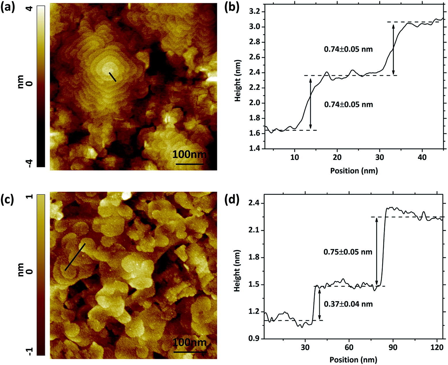 | ||
| Fig. 4 STM image of LSC113/214 VAN structure surface on (a) STO (001) and (c) GDC/YSZ (001) at room temperature. Imaging condition: Vbias = 2.5 V, Itunnel = 500 pA. (b) and (d) height profiles of the black lines in the STM images in (a) and (c), respectively. | ||
3.2 Strain state of LSC113/214 VAN films
The 2θ − ω scans for the VAN films on STO (001) and YSZ (001) with GDC buffer layer are shown in Fig. 5. X-ray diffraction analysis revealed the films to be oriented with their c-axes perpendicular to the substrate. Only the 00l reflections of LSC113 and LSC214 are present in the diffraction pattern; no peaks from any other impurity phase or orientation were observed. However, when we compare this diffraction pattern with single phase reference films, both the LSC113 and LSC214 peaks in the VAN have shifted with respect to their corresponding single phase patterns, indicating that the vertical strain state in each phase is altered in the LSC113/214 VAN structure.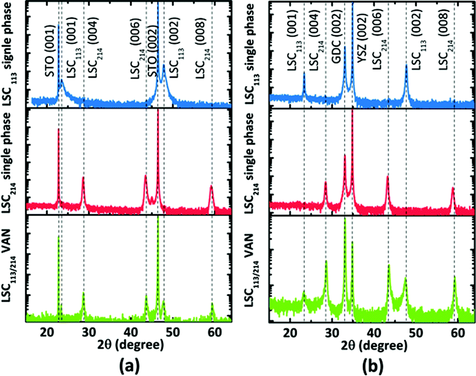 | ||
| Fig. 5 The 2θ − ω scans with logarithmic intensity scale of (a) LSC113, LSC214, and LSC113/214 VAN on STO (001) and (b) LSC113, LSC214, and LSC113/214 VAN on GDC/YSZ (001). The diffraction patterns show only the 00l diffraction peaks of LSC. | ||
Fig. 6a and b show the regions near the LSC113 (002) and LSC214 (006) peaks for the VAN films compared with the single phase films. For the single phase LSC113 and LSC214 films grown on GDC/YSZ (001), the out-of-plane lattice parameters are 3.810 Å and 12.540 Å, which are lower than the bulk values of 3.840 Å and 12.553 Å (found from X-ray powder diffraction measurement of the LSC113 and LSC214 targets used for PLD). The strain states of LSC films on STO and GDC/YSZ substrates are consistent with those reported in the literature.16,26,41 The strain state of the LSC/STO system can be explained by the lattice mismatch between film and substrate. But the origin of strain on LSC/GDC/YSZ is not well understood, since it cannot be explained by the confinement of the LSC film in plane by the GDC/YSZ (001) substrate, which would result in an opposite strain state at room temperature. It might be a consequence of different thermal expansion coefficients between the YSZ and LSC films as la O' et al. pointed out in their report.41 The physical origin of the strain state of the LSC films on YSZ substrate is out of the scope of this paper.
 | ||
| Fig. 6 X-ray diffraction data for the LSC113/214 VAN structure compared with single phase reference films of LSC113 and LSC214. 2θ − ω scans near the LSC113 (002) and LSC214 (006) of LSC113, LSC214, and LSC113/214 VAN on (a) STO (001) and (b) GDC/YSZ (001). The out-of-plane lattice constants versus calculated out-of-plane strain (with respect to bulk value) in LSC113, LSC214, and LSC113/214 VAN on (c) STO (001) and (d) GDC/YSZ (001). | ||
In the VAN structure, the out-of-plane lattice parameter is a direct indication of the strain state.42Fig. 6c and d show the out-of-plane lattice parameters of each phase (LSC113 and LSC214) in the VAN films versus the out-of-plane strain. Out-of-plane strain is calculated from the difference between the measured out-of-plane lattice parameter values for thin films and the known lattice parameter values for bulk. The results of the strain state on STO and YSZ substrates are very similar. The out-of-plane lattice parameter of LSC113 in the VAN structure is larger than that of the single phase LSC113, while the LSC214 phase has a smaller out-of-plane lattice parameter in the VAN structure than in the single phase reference film. This result shows that the vertical strain states of LSC113 and LSC214 have been changed in the VAN structure, with extra tensile (compressive) strain imposed to LSC113 (LSC214) within the respective domains. However, the interface strain state seems to be still mainly controlled by the lateral lattice mismatch between the film and the substrate. The transition from lateral strain control to vertical strain control depends on the geometry of the columnar grains. When the vertical interface area for a columnar grain exceeds the film/substrate interface area, the vertical strain would play a dominant role. Since this study is focusing on the correlation between electronic structure, surface chemistry and ORR kinetics, we aim to compare the results with the single phase reference films, which only have lateral strain and no vertical strain. Therefore, we retain the lateral strain state of the VAN films to be substrate controlled (just as in the single phase reference films) by keeping the film thickness (of 160 nm) less than the width of each column (300–500 nm).
3.3 Surface electronic structure of VAN films at room temperature
The phase assignment within the LSC113/214 composite is also confirmed by the tunneling current mapping and tunneling spectroscopy measurements (Fig. 7). Fig. 7a shows the tunneling current image with the zoomed-in topography image on the right. The contrast in the tunneling current image indicates the different conductivities of the respective regions: the regions with higher conductivity show the spiral growth pattern, while the darker regions have the layered structure. The tunneling spectroscopy (Fig. 7b) also shows the spiral grains to have an energy gap of about 1.5 ± 0.2 eV, while the layered region to have an energy gap of about 2.2 ± 0.3 eV and 2.1 ± 0.2 eV on STO and YSZ, respectively. Because LSC113 is more conducting and has a smaller energy gap than LSC214,18 we assign the spiral regions to be consisting of LSC113 and the layered regions to be consisting of LSC214. Our previous work has shown the LSC113 single phase surface energy gap to be 1.5 eV ± 0.2 eV,26 which is consistent with the LSC113 domains in the VAN structure here.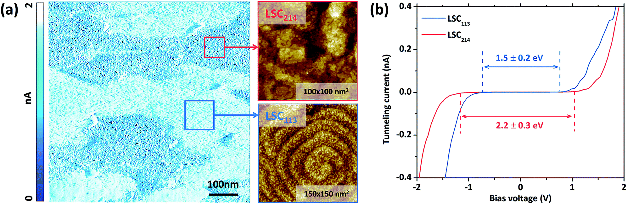 | ||
| Fig. 7 Electronic and topographic features of the surface of LSC113/214 VAN thin films on STO (001) (VAN/STO). (a) Tunneling feedback current map (negative image), with zoomed in topography. The contrast of the tunneling feedback current image indicates different conductivity and therefore different phase. (b) Tunneling current versus bias data on LSC113 and LSC214 domains. LSC113 domains in the VAN have a similar surface energy gap (1.5 ± 0.2 eV) as on the single phase LSC113 reference films, while LSC214 domains in the VAN have a measurable energy gap of 2.2 ± 0.3 eV. | ||
It should be noted that the STM measurements under room temperature conditions could not be successfully performed on the single phase LSC214 given its insulating nature. On the other hand, it was possible to perform STM and STS measurements on the LSC214 phase in the VAN film, and the energy gap at the surface is 2.2 ± 0.3 eV and 2.1 ± 0.2 eV on STO and YSZ, respectively. In addition, the energy gap is quite uniform over the LSC214 domains. STM of the LSC214 domains within the VAN film is assisted by the presence of LSC113 domains that increase the overall electronic conductivity of the composite film.
3.4 Surface electronic structure of VAN films at elevated temperature
Further investigation of the electronic structure of the film was carried out as a function of temperature. The energy gaps of LSC113 and LSC214 surfaces in the VAN structure were successively measured at room temperature, 100 °C, 200 °C, 250 °C, 300 °C and finally at room temperature again upon subsequent cooling from 300 °C, in 10−3 mbar of pure oxygen. The same measurements were also taken on the single phase reference films (Fig. 8a and b). The energy gap of LSC113 in the VAN and in the single phase film have a very similar behavior, going from 1.5 ± 0.2 eV at room temperature to metallic-like behavior with no energy gap at and above 250 °C. After cooling back down to room temperature, the energy gap recovers to 1.5 ± 0.2 eV, showing the reversibility of the semiconductor-metallic transition at the surface. The semiconductor-metallic transition arises from the creation of oxygen vacancy energy levels in the gap, as we reported in our previous work on LSC113 single phase thin films.26 | ||
| Fig. 8 Temperature dependence of the energy gap of (a) LSC113 and (b) LSC214 in single phase, multilayer and VAN/STO structure. Note that the surface energy gap variations with temperature in ML and VAN are quite similar for both LSC113 and LSC214 phases. The data on the multilayer system comes from ref. 18 and the data on the LSC113 comes from ref. 26. | ||
On the other hand, the temperature dependence of the energy gap at the surface of the LSC214 domains in the VAN structure is very different from that of the LSC214 single phase films. At and above 250 °C, the surface energy gap of LSC214 deviates from that on single phase LSC214 by about 1 eV. Comparing Fig. 8a and b, the electronic structure at the LSC214 surface in the VAN structure follows the LSC113 phase by becoming metallic-like above 250 °C. These results are consistent with the “electronic activation behavior” reported in our recent work for the LSC113/LSC214 multilayer structures (Fig. 8, ML data points18). At elevated temperatures, the LSC113 surface is easily reduced, forming oxygen vacancies.26 This serves to raise the electron chemical potential (Fermi level) and decrease the chemical potential of oxygen in the LSC113 phase.43 This would be expected to drive oxygen from LSC214 into LSC113 (ref. 44) and electrons from LSC113 to LSC214.18 The injection of electrons from LSC113 to LSC214 and the creation of defect states in LSC214 raises the Fermi level into the conduction band in the LSC214 phase, resulting in the disappearance of the energy gap as shown in Fig. 8b. Exchange of oxygen defects and electronic defects across the interfaces also enables charge neutrality over the width of the grain surfaces in the VAN.
3.5 Surface electrochemical activity of VAN films and electronic activation mechanism
All the electrochemical impedance spectra measured for LSC113, LSC214 and LSC113/214 VAN thin film electrodes consist of one dominating semicircle at low frequencies, an additional arc at intermediate frequencies and a non-zero intercept at the x-axis at higher frequencies. Fig. 9(a) shows a typical impedance spectrum obtained for the LSC113/214 VAN thin film electrode on GDC/YSZ in air. As shown in the inset, the spectrum can be modeled by a resistor in series with two R//Q circuits (R//Q: a resistor in parallel with a constant phase element, CPE). CPEs are used to take into account the possible heterogeneities in the electrodes resulting in “depressed” arcs not well represented by ideal capacitors.2 The offset resistance (R1) shows no pO2 or DC bias dependence and is characterized by an activation energy of 1.07 ± 0.07 eV, reflecting the YSZ ohmic contribution in series to the overall cell impedance. The additional arc between the offset resistance and the large semicircle at low frequencies also shows no pO2 dependence and is attributed to the ionic transfer resistance at the electrode/electrolyte interface. The real component of the low frequency impedance (R3) was found to increase with decreasing pO2, a feature typical of the oxygen exchange resistance.45 This assignment is further supported by the exceptionally large equivalent capacitance46 (2–5 mF cm−2), derived from CPE3 indicative of a chemical capacitance, as reported for other thin film MIEC systems.7,47 From the fitting procedure, the n-values of the CPE3 show no significant difference between the single-phase and VAN films, giving 0.84 ± 0.01 for LSC113, 0.81 ± 0.02 for LSC214 and 0.78 ± 0.04 for LSC113/214 VAN film cathodes, respectively.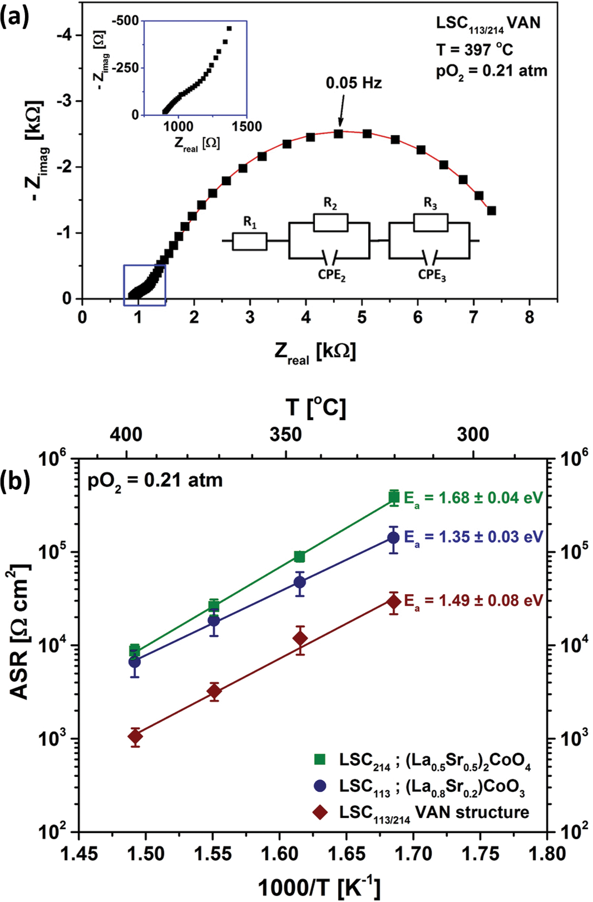 | ||
| Fig. 9 (a) A typical electrochemical impedance spectrum measured for an LSC113/214 VAN thin film electrode on GDC/YSZ (001) at 397 °C and in air. All the impedance spectra of LSC113 and LSC214 thin film electrodes show similar characteristics (Fig. S2†). The square dots are experimental data, while the solid line represents the best fit obtained with the equivalent circuit shown in the bottom inset. Variables of the circuit model are explained in the text. The top inset shows a magnification of the high frequency regime. (b) Temperature dependence of the area specific resistance (ASR) of oxygen surface exchange reaction at the surface of LSC113 and LSC214 single phase film electrodes and of LSC113/214 VAN film electrode measured in air and at 320 °C–397 °C. | ||
Fig. 9(b) shows the temperature dependence of the resistance of the surface to oxygen exchange, in terms of an area specific resistance (ASR) in air, derived from element R3, for the LSC113 and LSC214 single phase thin film electrodes and for the LSC113/214 VAN film electrode for the temperature range of 320–397 °C. The ORR activity of VAN film electrodes, which is inversely related to this surface exchange ASR, is clearly seen to be enhanced by about one order of magnitude, compared to that of the LSC113 and LSC214 single phase electrodes. The range of the derived activation energies, 1.35–1.68 eV, are similar to those previously reported for LSC electrodes.13,27,48–52 However, the enhanced ORR activity disappears at higher temperatures, in the range of 445 °C to 620 °C in this work. Fig. 10 shows the temperature dependence of the ASR of the LSC113 single phase and LSC113/214 VAN film electrodes measured in air and at temperatures of 445 °C–546 °C. The ASR is observed to systematically increase at the initial temperature of 445 °C during subsequent measurements taken 30 minutes apart. After the ASR reached a stable value, the measurement temperature was increased up to 546 °C and then decreased back to 445 °C. The surface exchange ASR of the LSC113 single phase and of the LSC113/214 VAN films reached similar values during this process, a signature of the degradation of the surface activity of both the LSC113 and LSC113/214 VAN electrodes. The next section will present the evolution of the surface cation composition and microstructure to explain this degradation process.
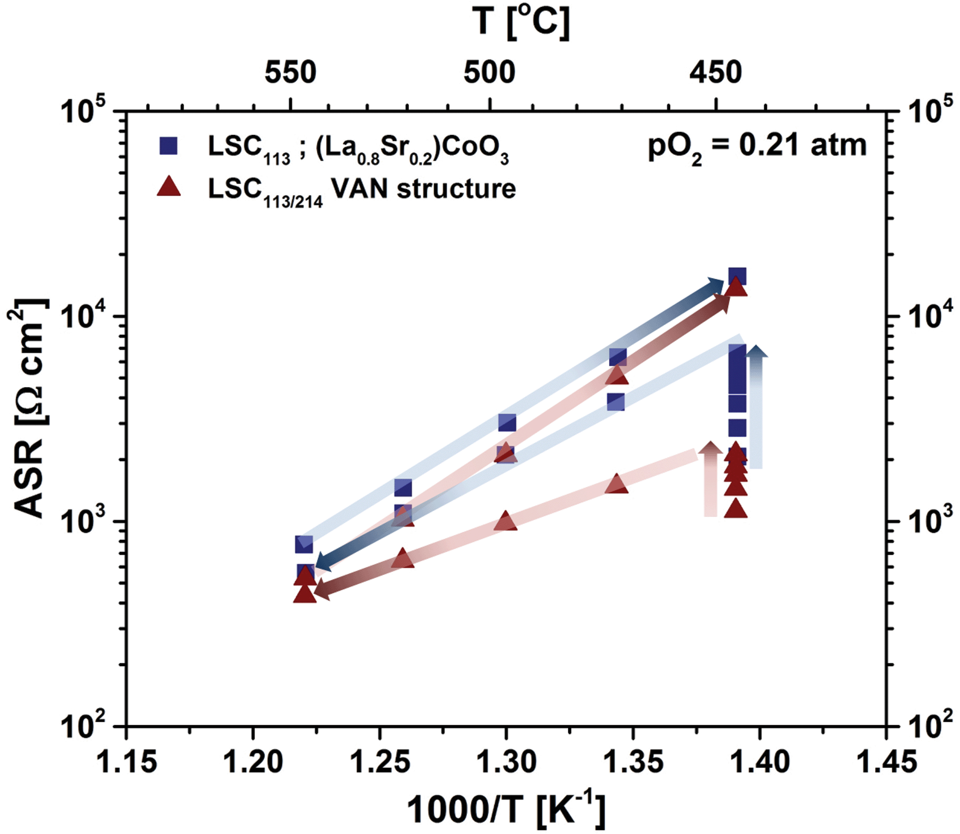 | ||
| Fig. 10 Temperature dependence of the area specific resistance (ASR) of LSC113 single phase film electrode (blue squares) and of LSC113/214 VAN film electrode (red triangles) measured in air and at 445 °C–546 °C. The blue and red arrows indicate the measurement sequence on the LSC113 single phase and the LSC113/214 VAN film electrodes, respectively. The ASR was monitored while the samples were kept at 445 °C during measurements taken 30 minutes apart. After the ASR reached a stable value at 445 °C, the measurement temperature was increased up to 546 °C and then decreased back to 445 °C. | ||
3.6 Evolution of surface microstructure and cation chemistry upon thermal annealing
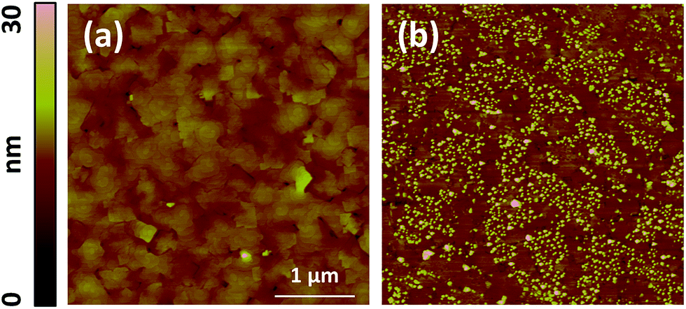
The electrochemical impedance results indicate a significant degradation of the surfaces at elevated temperatures, above 400 °C (specifically shown at 450–620 °C in this work). This degradation of the surface reactivity suggests some form of chemical aging at the surface as reported for LSC by Kubicek et al.53 and by us54 earlier. To identify the source of the degradation on LSC113/214 VAN films at elevated temperatures, an equivalent set of as-prepared LSC113/214 VAN and single phase LSC113 and LSC214 reference samples were annealed for 10 hours at 370 °C and at 620 °C in air, using the same setup and conditions as in the EIS measurements. These were subsequently subjected to AFM and XPS analysis to examine how the surface microstructure and chemistry evolves at elevated temperatures.As shown Fig. 11a, the as-prepared LSC113 single phase film was characterized by a smooth surface with grains of a few hundreds of nm wide. While no change in surface morphology was detected in AFM following annealing at 370 °C (Fig. 11b), smaller particles appeared across the entire surface (some preferentially at grain boundaries) after annealing at 620 °C (Fig. 11c). As-prepared LSC214 single phase film, on the other hand, showed a rougher grain structure (Fig. 11d). After thermal annealing at 620 °C in air, the surface became relatively less rough but many particles evidently remain (Fig. 11f) at the surface. Within the resolution limit of the AFM image, the surface morphology and roughness of the VAN film annealed at 370 °C does not change from the as-prepared state (Fig. 11g and h). However, the surface roughness increases, along with the formation of large particles at the surface and the disappearance of the spiral domain, after annealing at 620 °C. Interestingly, the areas where the particles are formed can be clearly separated by the area without the particles (as seen in Fig. 12b), indicating that part of the film surface is not segregating. By comparing the size and shape of the film features (i.e. disappearance of the spiral patterns, and the remaining flat faceted/cornered features in Fig. 12b), the area with and without particles can be assigned to LSC113 and LSC214 domains, respectively, on the VAN film. This indicates that the presence of LSC113 domains enables a more stable LSC214 surface that does not form precipitated particles neither at the as-prepared state and nor at the annealed state.
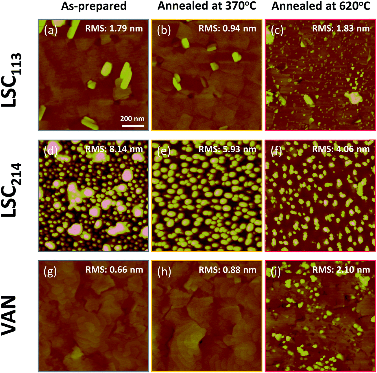 | ||
| Fig. 11 Atomic force microscopy images (1 μm × 1 μm) of the LSC113/214 VAN, LSC113 and LSC214 films on GDC/YSZ (001) substrate at different conditions: as-prepared, annealed for 10 hours at 370 °C and at 620 °C in air. The common height-scale for each image is 0–30 nm. | ||
 | ||
| Fig. 12 Atomic force microscopy images (5 μm × 5 μm) of the LSC113/214 VAN films on GDC/YSZ (001) substrate at different conditions: (a) as-prepared and (b) annealed for 10 hours at 620 °C in air. | ||
The surface roughening in the VAN film is accompanied by a sharp enrichment of the A-site cations (La and Sr), i.e. a larger (Sr + La)/Co ratio (Fig. 13g and i) at/near the surface. Furthermore, as shown from the increase of the (Sr + La)/Co quantity from 0° (deeper into the bulk by 6 nm) to 70° (within 2 nm of the surface), the enrichment of the A-site cations at 620 °C is originating at/near the surface of the VAN films, concurrent with the formation of the particles shown in Fig. 11 and 12. Similarly to our and others' previous findings,29,54,55 such A-site enrichment exists in the formation of insulating phases,54,56,57 as also seen in this work from the AFM images (Fig. 11 and 12) and from the analysis of the Sr 3d spectrum (Fig. S1†). Such chemical, electronic and phase changes at the surface contribute to surface reactivity degradation of the perovskite and perovskite-related phases, and thus, slows the ORR kinetics at the surface of the LSC113/214 VAN films as found in our EIS experiments.
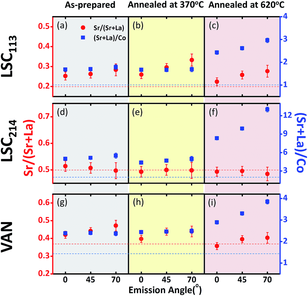 | ||
| Fig. 13 Sr/(Sr + La) and (Sr + La)/Co ratios deduced from X-ray photoelectron spectroscopy measurement and analysis of the La 4d, Sr 3d, La 3d and Co 2p emissions, on the VAN, LSC113 and LSC214 films that are in the as-prepared state and that were annealed at 370 °C and at 620 °C in air for 10 hours. The photo-electron emission angles of 0°, 45° and 70° indicate the depth sensitivity, going from deeper to more surface sensitive signals, respectively. The determination of bulk nominal Sr/(Sr + La) and (Sr + La)/Co values for VAN are based on the 3:2 molar ratio of LSC113 and LSC214 in LSC113/214 composite target (see Section 2. Experimental methods). | ||
Very interestingly, comparison of the cation composition on the LSC113/214 VAN film with that on the single phase LSC113 and LCS214 reference films reveals that the VAN surface is chemically more stable than the surfaces of LSC214 and LSC113 alone. The magnitude of the total A-site cation enrichment, denoted by the (Sr + La)/Co ratio, at the VAN film surface at 620 °C is (∼4) much smaller than that of the LSC214 (∼12) and closer to that of the LSC113 surface (∼3) (Fig. 13c, f and i). Sr enrichment at the A-site, denoted by the Sr/(Sr + La) ratio, at the VAN surface is close to the bulk nominal value both at 370 °C and 620 °C, while that on LSC113 is greater than the bulk nominal level. This result indicates that the LSC113 phase in the VAN structure may also play a role in stabilizing the (La + Sr)/Co ratio and avoid (or minimize) phase separation of Sr- and La-rich oxides at the LSC214 domain surface. At the same time, the total Sr enrichment at the surface is suppressed on the VAN surface. These signatures of chemical stabilization can also contribute to a superior electrochemical performance of the LSC113/214 VAN films.
4. Discussion
This work had two motivations: (1) to examine the validity of the electronic activation mechanism in a columnar composite made of LSC113/214 that provides a more controlled structure for embedding hetero-interfaces in cathodes, and (2) to uncover whether there are any additional mechanisms that contribute to the enhancement of the ORR reactivity of the LSC113/214 hetero-system in a structure that is feasible for electrochemical measurements. The vertically aligned nanocomposite made of LSC113/214 provided the means to probe both of these purposes in this work.From the tunneling spectroscopy measurements (Fig. 7), we confirmed that the LSC214 phase in the VAN structure is electronically activated, in a similar way as was shown within the LSC113/214 multilayers in our recent work.18 The effective activation area extends to the entire LSC214 domains whose dimensions ranges from 50 to 300 nm. Such large spatial extent of electronic activation could be explained by electron injection18 accompanied by exchange of charged oxygen defects (oxygen vacancies and interstitials)28,44 at LSC113/214 interfaces that enables long-range charge neutrality in the system.
The apparent electronic activation of the LSC214 domains in the VAN structure is expected to have the following impact on the ORR kinetics. The upshift of the Fermi level that leads to the disappearance of the energy gap on LSC214 in VAN at elevated temperatures (250–300 °C) represents a larger concentration of free electrons on this originally p-type material, leading to faster oxygen reduction kinetics on LSC214 domains. In this study, we observed 10 times enhancement of ORR kinetics instead of 3 orders of magnitude as reported in the literature.14,15 One of the reasons for the lesser enhancement could be the strongly anisotropic structure and oxygen incorporation properties of LSC214. Given that the LSC214 [100] direction, which is the fast oxygen incorporation and transport path, is parallel to the sample surface, the VAN structure on YSZ (001) substrate could not benefit from the 102 times ORR enhancement predicted by Han and Yildiz due to the anisotropic oxygen incorporation kinetics through LSC214 (100) channel.20
The combined XPS, AFM and EIS measurements on the LSC113, LSC214 and LSC113/214 VAN film electrodes revealed the superior stability of the cation composition on the LSC113/214 VAN surface could be another source of the higher ORR activity. The reduced enrichment of Sr and La cations at the surface of the VAN films allows for more pristine perovskite and Ruddlesden Popper terminations, and minimizes or partially avoids the coverage of the surface by insulating phases such as Sr- and La-rich oxides or hydroxides that block the ORR kinetics. The LSC113/214 VAN structure films are stable at lower temperatures (320–400 °C). At higher temperatures, on the other hand, all the films, including the LSC113/214 VAN film, suffered from a strong time-dependent degradation. Although the surface chemistry of the VAN is more stable than the single phase films, it is sufficiently segregated that the degradation of the ORR kinetics is still quite evident. Based on the electronic activation and the decrease of the detrimental surface segregation found at the VAN surface in this work, future work that identifies more stable hetero-structures while retaining the electronic coupling is warranted.
We have shown that the VAN arrangement of the LSC perovskite and Ruddlesden-Popper phases resulted in the generation of line defects (screw dislocations) perpendicular to the surface of the VAN structure in the LSC113 domains (Fig. 4 and 7). The density of screw dislocations is about N = 60 μm−2 as counted from the STM images. We note that the effect of such line defects on the surface ORR kinetics is still not clear. If we assume that the ORR kinetics enhancement is only due to the screw dislocations, then we could get an estimation of the relative enhancement at the dislocations based on the following equation: ϕkdislchem + (1 − ϕ)kLSCchem = kVANchem = 10 × kLSCchem, where ϕ is the percentage of dislocation activated area, kchem is the chemical surface exchange coefficient. Assuming the activation radius of each dislocation is r = 1–3 nm, then ϕ = N × π × r2 is about 10−4 – 10−3, which gives kdislchem ≈104 to 105 × kLSCchem. Thus, the ORR kinetics would be expected to have at least four or five order of magnitude enhancement at dislocations in order to obtain one order of magnitude overall enhancement. There is no evidence showing such surface ORR enhancement by screw dislocations in the literature. Therefore, we could not attribute the 10 times ORR kinetics improvement entirely to the effect of screw dislocations.
The VAN structure has shown potential as a high performance intermediate temperature SOFC cathode. Some aspects still need to be improved to further enhance the overall ORR kinetics. First of all, as mentioned in the discussion of the electronic activation mechanism, the fast oxygen incorporation path, LSC214 (100), is lying parallel to the surface instead of normal to the surface. By synthesizing LSC214 (100) vertical to the surface in the VAN structure and by finding ways to avoid detrimental cation segregation at the surface, we could expect further enhancement of ORR kinetics, besides the electronic activation enhancement. Chemically optimizing the doping levels of both the A- and B-site cations or exploring other coupled perovskite/Ruddlesden-Popper material systems, to get better electronic and ionic conductivity and stability, also provides unlimited opportunities to further improve the ORR kinetics. The control of microstructure could be achieved by varying deposition parameters, substrate interface and ratio of phase composition. Additional treatment of VAN structure, either by thermal annealing in varying oxygen pressures or by selective etching, could also be an effective way to tailor desirable microstructural and chemical properties for higher ORR activity.
5. Conclusion
Vertically aligned nanocomposites LSC113/214 were synthesized and examined with respect to their electronic structure, surface chemistry and electrochemical performance. A number of interesting features that relate to the performance of these VAN films were found. Vertically aligned nano-scale columns of LSC113 and LSC214 were formed coherently on the STO (001) and YSZ/GDC (001) substrates. The surface electronic structure of LSC214 in VAN was modified compared to single phase LSC214 films. Upon the onset of reduction in LSC113 at 250 °C and above, the exposed LSC214 grain surfaces were found to be electronically activated, with a complete disappearance of the energy gap in contrast to the ∼0.7–1 eV energy gap at the surface of the single phase LSC214 films, as detected by in situ STM and STS. Electrochemical impedance analysis showed a 10-fold increase of surface oxygen exchange kinetics on the LSC113/214 VAN cathodes compared to the LSC113 and LSC214 single phase film cathodes at 320–400 °C, demonstrating improved performance enabled by the hetero-interfaces in a controlled microstructure. Combined XPS, AFM and EIS measurements also revealed superior stability of the cation composition on the LSC113/214 VAN film compared to the detrimental segregation and phase separation of Sr- and La-rich phases at the surfaces of the LSC113 and LSC214 single phase films. Both the electronic activation and the relatively more stable cation composition at the LSC113/214 VAN films are likely to be mechanisms that render these hetero-systems more highly reactive to oxygen reduction reaction. However, above 400 °C, the stability of the surface chemistry of the LSC113/214 heterosystem appears to become an issue, leading to the degradation of the oxygen reduction kinetics.In concluding, we identify the VAN composite structure as a highly promising approach for achieving enhanced cathode performance and stability. While the LSC113/214 composite shows reduced detrimental segregation and phase separation of Sr- and La-rich phases at its surfaces, nevertheless, the degradation of the surface remains significant at temperatures above 400 °C. This stability issue arises because of intrinsic properties of the LSC113/214 composition itself, and is not because of the VAN structure. This finding is particularly significant since the instability of the LSC113/214 hetero-structure was not previously discussed in the works of Sase et al.14,15 and Crumlin et al.16,58 that focused only on the initial performance of this composite. While this is a partially negative finding, it aids in directing future research towards the identification of alternatives that are inherently more stable, while retaining their high reactivity to ORR. Furthermore, within our knowledge, this is the first study to adopt a vertically aligned nano-structure composite designed to enhance the electrochemical activity by virtue of the formation of internal hetero-interfaces. These interfaces offer means for further enhancing the ORR activity of the LSC214 phase by enhancing its charge transfer capability and minimizing La and Sr segregation to its surface. Such VAN composite structures enable finer tuning of reactivity and stability by control of orientation, strain and phase fraction of each of the phases within the composite film. Work is ongoing by the authors to identify more highly stable hetero-structure VAN compositions with high ORR reactivity.
Acknowledgements
This work was supported by the US-DOE Basic Energy Sciences, Grant no. DE-SC0002633 at MIT. The cross sectional SEM, X-ray diffraction, X-ray photoelectron spectroscopy and Auger electron spectroscopy measurements were performed at the Center of Materials Science and Engineering, an NSF MRSEC facility at MIT. T. D. and K. S. acknowledge financial support from the Progress-100 program at Kyushu University. JJK thanks the Kwanjeong Educational Foundation for fellowship support.References
- B. C. H. Steele and A. Heinzel, Nature, 2001, 414, 345–352 CrossRef CAS PubMed.
- S. B. Adler, Chem. Rev., 2004, 104, 4791–4843 CrossRef CAS.
- H. A. Gasteiger and N. M. Markovic, Science, 2009, 324, 48–49 CrossRef CAS PubMed.
- W. Jung and H. L. Tuller, Adv. Energy Mater., 2011, 1, 1184–1191 CrossRef CAS.
- K. T. Lee and A. Manthiram, J. Electrochem. Soc., 2005, 152, A197–A204 CrossRef CAS PubMed.
- N. P. Brandon, S. Skinner and B. C. H. Steele, Annu. Rev. Mater. Res., 2003, 33, 183–213 CrossRef CAS.
- F. S. Baumann, J. Fleig, H. U. Habermeier and J. Maier, Solid State Ionics, 2006, 177, 1071–1081 CrossRef CAS PubMed.
- E. D. Wachsman and K. T. Lee, Science, 2011, 334, 935–939 CrossRef CAS PubMed.
- R. Merkle and J. Maier, Angew. Chem., Int. Ed., 2008, 47, 3874–3894 CrossRef CAS PubMed.
- M. M. Kuklja, E. A. Kotomin, R. Merkle, Y. A. Mastrikov and J. Maier, Phys. Chem. Chem. Phys., 2013, 15, 5443–5471 RSC.
- M. T. Greiner, M. G. Helander, W. M. Tang, Z. B. Wang, J. Qiu and Z. H. Lu, Nat. Mater., 2012, 11, 76–81 CrossRef CAS PubMed.
- N. A. Deskins, R. Rousseau and M. Dupuis, J. Phys. Chem. C, 2010, 114, 5891–5897 CAS.
- J. Hayd, H. Yokokawa and E. Ivers-Tiffee, J. Electrochem. Soc., 2013, 160, F351–F359 CrossRef CAS PubMed.
- M. Sase, F. Hermes, K. Yashiro, K. Sato, J. Mizusaki, T. Kawada, N. Sakai and H. Yokokawa, J. Electrochem. Soc., 2008, 155, B793–B797 CrossRef CAS PubMed.
- M. Sase, K. Yashiro, K. Sato, J. Mizusaki, T. Kawada, N. Sakai, K. Yamaji, T. Horita and H. Yokokawa, Solid State Ionics, 2008, 178, 1843–1852 CrossRef CAS PubMed.
- E. J. Crumlin, E. Mutoro, S. J. Ahn, G. J. la O', D. N. Leonard, A. Borisevich, M. D. Biegalski, H. M. Christen and Y. Shao-Horn, J. Phys. Chem. Lett., 2010, 1, 3149–3155 CrossRef CAS.
- K. Yashiro, T. Nakamura, M. Sase, F. Hermes, K. Sato, T. Kawada and J. Mizusaki, Electrochem. Solid-State Lett., 2009, 12, B135–B137 CrossRef CAS PubMed.
- Y. Chen, Z. Cai, Y. Kuru, W. Ma, H. L. Tuller and B. Yildiz, Adv. Energy Mater., 2013, 3, 1221–1229 CrossRef CAS.
- A. Kushima, D. Parfitt, A. Chroneos, B. Yildiz, J. A. Kilner and R. W. Grimes, Phys. Chem. Chem. Phys., 2011, 13, 2242–2249 RSC.
- J. W. Han and B. Yildiz, Energy Environ. Sci., 2012, 5, 8598–8607 CAS.
- O. I. Lebedev, J. Verbeeck, G. Van Tendeloo, O. Shapoval, A. Belenchuk, V. Moshnyaga, B. Damashcke and K. Samwer, Phys. Rev. B: Condens. Matter Mater. Phys., 2002, 66, 104421 CrossRef.
- Z. Bi, J. H. Lee, H. Yang, Q. Jia, J. L. MacManus-Driscoll and H. Wang, J. Appl. Phys., 2009, 106, 094309 CrossRef PubMed.
- A. P. Chen, Z. X. Bi, Q. X. Jia, J. L. MacManus-Driscoll and H. Y. Wang, Acta Mater., 2013, 61, 2783–2792 CrossRef CAS PubMed.
- J. Yoon, S. Cho, J. H. Kim, J. Lee, Z. X. Bi, A. Serquis, X. H. Zhang, A. Manthiram and H. Y. Wang, Adv. Funct. Mater., 2009, 19, 3868–3873 CrossRef CAS.
- Q. Su, D. Yoon, A. P. Chen, F. Khatkhatay, A. Manthiram and H. Y. Wang, J. Power Sources, 2013, 242, 455–463 CrossRef CAS PubMed.
- Z. H. Cai, Y. Kuru, J. W. Han, Y. Chen and B. Yildiz, J. Am. Chem. Soc., 2011, 133, 17696–17704 CrossRef CAS PubMed.
- J. Januschewsky, M. Ahrens, A. Opitz, F. Kubel and J. Fleig, Adv. Funct. Mater., 2009, 19, 3151–3156 CrossRef CAS.
- Y. Chen, D. Fong, W. Herbert, J. P. Rueff, N. Tsvetkov and B. Yildiz, 2014, in preparation.
- Y. Chen, W. Jung, Z. H. Cai, J. J. Kim, H. L. Tuller and B. Yildiz, Energy Environ. Sci., 2012, 5, 7979–7988 CAS.
- H. Jalili, J. W. Han, Y. Kuru, Z. H. Cai and B. Yildiz, J. Phys. Chem. Lett., 2011, 2, 801–807 CrossRef CAS.
- M. Kakihana and M. Yoshimura, Bull. Chem. Soc. Jpn., 1999, 72, 1427–1443 CrossRef CAS.
- NIST Database 82, U.S. Department of Commerce, Washington, DC, 2001 Search PubMed.
- V. V. Vashook, H. Ullmann, O. P. Olshevskaya, V. P. Kulik, V. E. Lukashevich and L. V. Kokhanovskij, Solid State Ionics, 2000, 138, 99–104 CrossRef CAS.
- A. Petric, P. Huang and F. Tietz, Solid State Ionics, 2000, 135, 719–725 CrossRef CAS.
- R. L. Penn and J. F. Banfield, Science, 1998, 281, 969–971 CrossRef CAS.
- M. Hawley, I. D. Raistrick, J. G. Beery and R. J. Houlton, Science, 1991, 251, 1587–1589 CAS.
- W. K. Burton, N. Cabrera and F. C. Frank, Phil. Trans. Roy. Soc. Lond. Math. Phys. Sci., 1951, 243, 299–358 CrossRef.
- Y. G. Li and Y. Y. Wu, Chem. Mater., 2010, 22, 5537–5542 CrossRef CAS.
- S. A. Morin, M. J. Bierman, J. Tong and S. Jin, Science, 2010, 328, 476–480 CrossRef CAS PubMed.
- F. Meng, S. A. Morin, A. Forticaux and S. Jin, Acc. Chem. Res., 2013, 46, 1616–1626 CrossRef CAS PubMed.
- G. J. la O', S.-J. Ahn, E. Crumlin, Y. Orikasa, M. D. Biegalski, H. M. Christen and Y. Shao-Horn, Angew. Chem., Int. Ed., 2010, 49, 5344–5347 CrossRef PubMed.
- J. L. MaCmanus-Driscoll, P. Zerrer, H. Y. Wang, H. Yang, J. Yoon, A. Fouchet, R. Yu, M. G. Blamire and Q. X. Jia, Nat. Mater., 2008, 7, 314–320 CrossRef CAS PubMed.
- M. V. Ganduglia-Pirovano, A. Hofmann and J. Sauer, Surf. Sci. Rep., 2007, 62, 219–270 CrossRef CAS PubMed.
- N. Tsvetkov, Y. Chen and B. Yildiz, J. Mater. Chem. A, 2014, 2, 14690–14695 CAS.
- W. C. Chueh and S. M. Haile, Annu. Rev. Chem. Biomol. Eng., 2012, 3, 313–341 CrossRef CAS PubMed.
- J. Fleig, Solid State Ionics, 2002, 150, 181–193 CrossRef CAS.
- W. Jung and H. L. Tuller, J. Electrochem. Soc., 2008, 155, B1194–B1201 CrossRef CAS PubMed.
- F. P. F. van Berkel, S. Brussel, M. van Tuel, G. Schoemakers, B. Rietveld and P. V. Aravind, Proceedings of the 7th European Solid Oxide Fuel Cell Forum, ed. J. A. Kilner, 2006, p. 1 Search PubMed.
- S. B. Adler, Solid State Ionics, 1998, 111, 125–134 CrossRef CAS.
- A. Heel, P. Holtappels and T. Graule, J. Power Sources, 2010, 195, 6709–6718 CrossRef CAS PubMed.
- C. Peters, A. Weber and E. Ivers-Tiffee, J. Electrochem. Soc., 2008, 155, B730–B737 CrossRef CAS PubMed.
- S. Wang, J. Yoon, G. Kim, D. Huang, H. Wang and A. J. Jacobson, Chem. Mater., 2010, 22, 776–782 CrossRef CAS.
- M. Kubicek, A. Limbeck, T. Fromling, H. Hutter and J. Fleig, J. Electrochem. Soc., 2011, 158, B727–B734 CrossRef CAS PubMed.
- Z. H. Cai, M. Kubicek, J. Fleig and B. Yildiz, Chem. Mater., 2012, 24, 1116–1127 CrossRef CAS.
- W. Lee, J. W. Han, Y. Chen, Z. H. Cai and B. Yildiz, J. Am. Chem. Soc., 2013, 135, 7909–7925 CrossRef CAS PubMed.
- P. A. W. van der Heide, Surf. Interface Anal., 2002, 33, 414–425 CrossRef CAS.
- J. C. Dupin, D. Gonbeau, P. Vinatier and A. Levasseur, Phys. Chem. Chem. Phys., 2000, 2, 1319–1324 RSC.
- E. J. Crumlin, E. Mutoro, Z. Liu, M. E. Grass, M. D. Biegalski, Y. L. Lee, D. Morgan, H. M. Christen, H. Bluhm and Y. Shao-Horn, Energy Environ. Sci., 2012, 5, 6081–6088 CAS.
Footnote |
| † Electronic supplementary information (ESI) available. See DOI: 10.1039/c4ta04993d |
| This journal is © The Royal Society of Chemistry 2015 |