DOI:
10.1039/C5SC00708A
(Edge Article)
Chem. Sci., 2015,
6, 4615-4622
Shape and composition control of Bi19S27(Br3−x,Ix) alloyed nanowires: the role of metal ions†
Received
26th February 2015
, Accepted 13th May 2015
First published on 13th May 2015
Abstract
We present the first colloidal synthesis of highly uniform single-crystalline Bi19S27Br3 nanowires (NWs) with a mean diameter of ∼9 nm and tunable lengths in the range of 0.15–2 μm in the presence of foreign metal ions (Al3+). The Al3+ ions not only control the growth of NWs, but also achieve species transformation, i.e., from Bi2S3 to Bi19S27Br3, and are not present in the resulting NWs. This colloidal chemistry approach can be expanded to prepare a family of single-crystalline Bi19S27(Br3−x,Ix) alloyed NWs with controlled compositions (0 ≤ x ≤ 3). Interestingly, these alloyed NWs show an unusual composition-independent band gap of ∼0.82 eV, and theoretical calculations indicate that this phenomenon comes from the very minor contributions of the halogens to the valence band maximum and conduction band minimum. The photodetectors made of Bi19S27(Br3−x,Ix) alloyed NWs show a pronounced photoresponse with high stability and reproducibility, which makes the NWs potentially useful candidates in optoelectronic devices.
Introduction
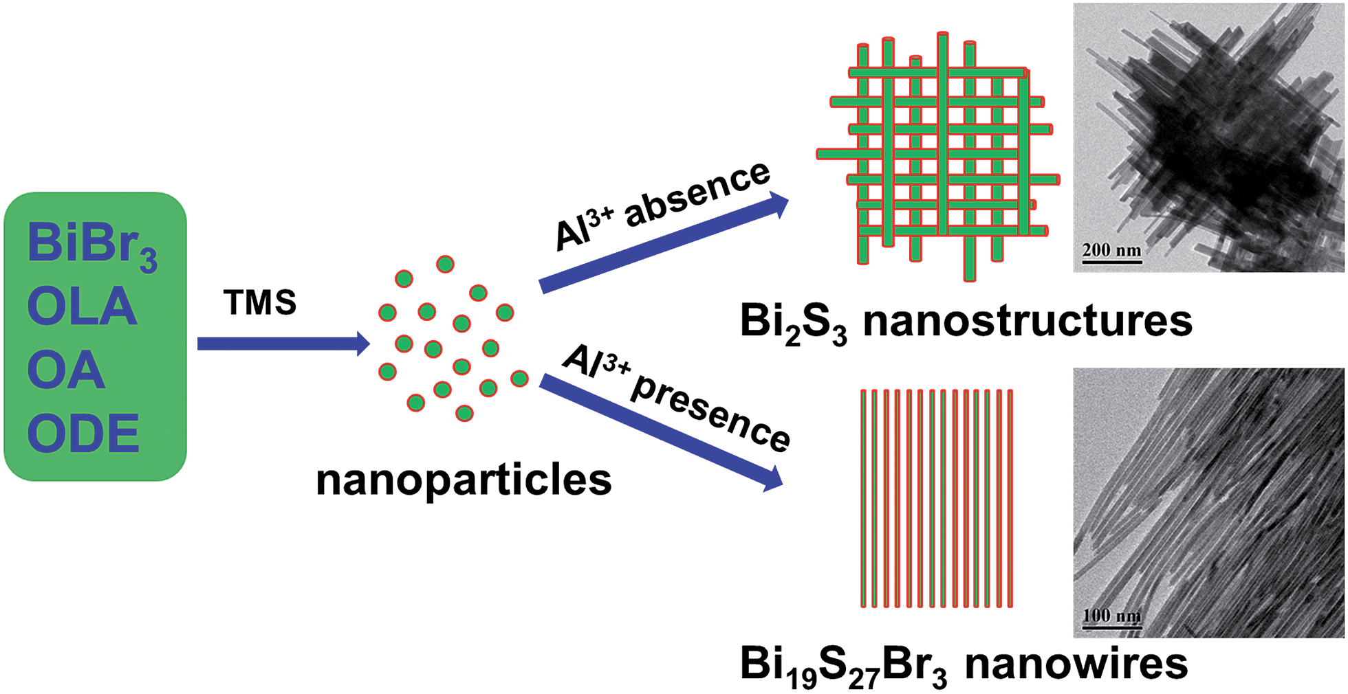
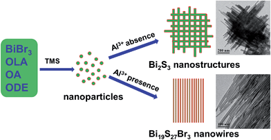
Semiconductor nanowires (NWs),1 which are key building blocks for the next generation of optoelectronic devices such as light-emitting diodes (LEDs),2 solar cells,3 photodetectors,4 field-effect transistors (FETs),5 thermoelectric devices6 and so on, have been extensively studied due to their anisotropic geometry, large surface-to-volume ratio, their decoupling of light absorption and minority carrier diffusion directions for efficient charge collection and separation, and their exciton confinement in two dimensions that are superior to their bulk counterparts. Moreover, semiconductor NWs have various mechanical properties and reactivities which depend on the crystallographic orientation.7 Considerable efforts have been made to exploit their useful properties and widen their applications, and especially to improve their synthesis1a,8 by metal-nanoparticle-mediated methods,9 direct deposition methods,10 template-directed methods,11 and oriented-attachment methods in colloidal chemistry.12 Colloidal synthesis, which takes advantage of the versatility of the precursors, ligand affinity, solvent polarity, and reaction parameters, has been demonstrated to be a powerful strategy for exploiting colloidal nanocrystals (NCs) with controlled phases,13 morphology14 and composition15 for binary and ternary systems. The superiority of colloidal chemistry has also been demonstrated in the synthesis of very interesting semiconducting heterostructured NCs.16 In contrast, the controllable synthesis of quaternary and quinary alloyed NCs is much more difficult, and the synthesis of multi-component NWs is an even bigger challenge than nanoparticles. Generally, long carbon chain organic molecules that selectively bind to different NC facets are used to control the morphology of the resulting NCs.17 More recently, inorganic foreign metal ions have been employed to influence the morphology of semiconductor NCs (CuxSe and CuTe NCs),18 which may provide a new way to control the shape of NCs. However, no success has been reported on the formation of one-dimensional nanomaterials mediated by foreign metal ions up to date, let alone multi-component NWs. This inspired us to employ this strategy to exploit a new type of multi-component semiconductor NW, which may greatly expand the research platform in this field.
A group of BiIIIVIAVIIA compounds, BiOCl, BiSCl, Bi19S27Br3, and BiSI, has provoked great research interest varying from catalysis to electronics due to their promising properties, such as their optoelectronic effect, photoconductivity, ferroelectricity, piezoelectricity, electromechanical effect, and a large temperature dependence of the band gap.19 Traditionally, these semiconductors with poorly defined morphology were synthesized via vapor-phase growth at high temperature (>600 °C), which usually required specialized and complicated facilities and even toxic H2S and HBr.20 Solvothermal methods have been exploited to prepare bundle–rod-like Bi19S27Br3.19c A microwave-assisted aqueous synthesis has recently been developed to prepare fabric-like Bi19S27Br3 superstructures with large diameters (∼80 nm) and their photocatalytic performance has also been investigated.19d However, to the best of our knowledge, the controllable synthesis of single-crystalline Bi19S27Br3 colloidal NWs with uniform morphology remains undeveloped, hindering the understanding of their fundamental properties and the exploitation of their potential applications. Herein we present a facile, colloidal approach to well-defined Bi19S27Br3 NWs by using Al3+ ions to mediate the oriented growth of Bi19S27Br3. We have demonstrated that aluminum(III) acetylacetonate [Al(acac)3] not only controls the growth of NWs, but also achieves species transformation, i.e., from Bi2S3 to Bi19S27Br3. We have further expanded this foreign metal ion mediated approach to realize the synthesis of uniform quaternary Bi19S27(Br3−x,Ix) NWs with compositions varying across the entire range (0 ≤ x ≤ 3). Full experimental details can be found in the ESI.† Their microstructures and properties were thoroughly characterized by a variety of analyses, such as X-ray diffraction (XRD), X-ray photoelectron spectroscopy (XPS), Raman spectra, scanning electron microscopy (SEM), transmission electron microscopy (TEM), high-resolution transmission electron microscopy (HRTEM), and UV-visible-near-infrared (UV-vis-NIR) absorption spectroscopy. It is very interesting to find that these alloyed NWs show an unusual composition-independent band gap, which differs from the widely accepted Vegard's law for multi-component alloyed semiconductors.21 The application potential of Bi19S27(Br3−x,Ix) NWs in photoelectronics was finally assessed by fabricating photodetectors (PDs), showing a pronounced photoresponse with high stability.
Results and discussion
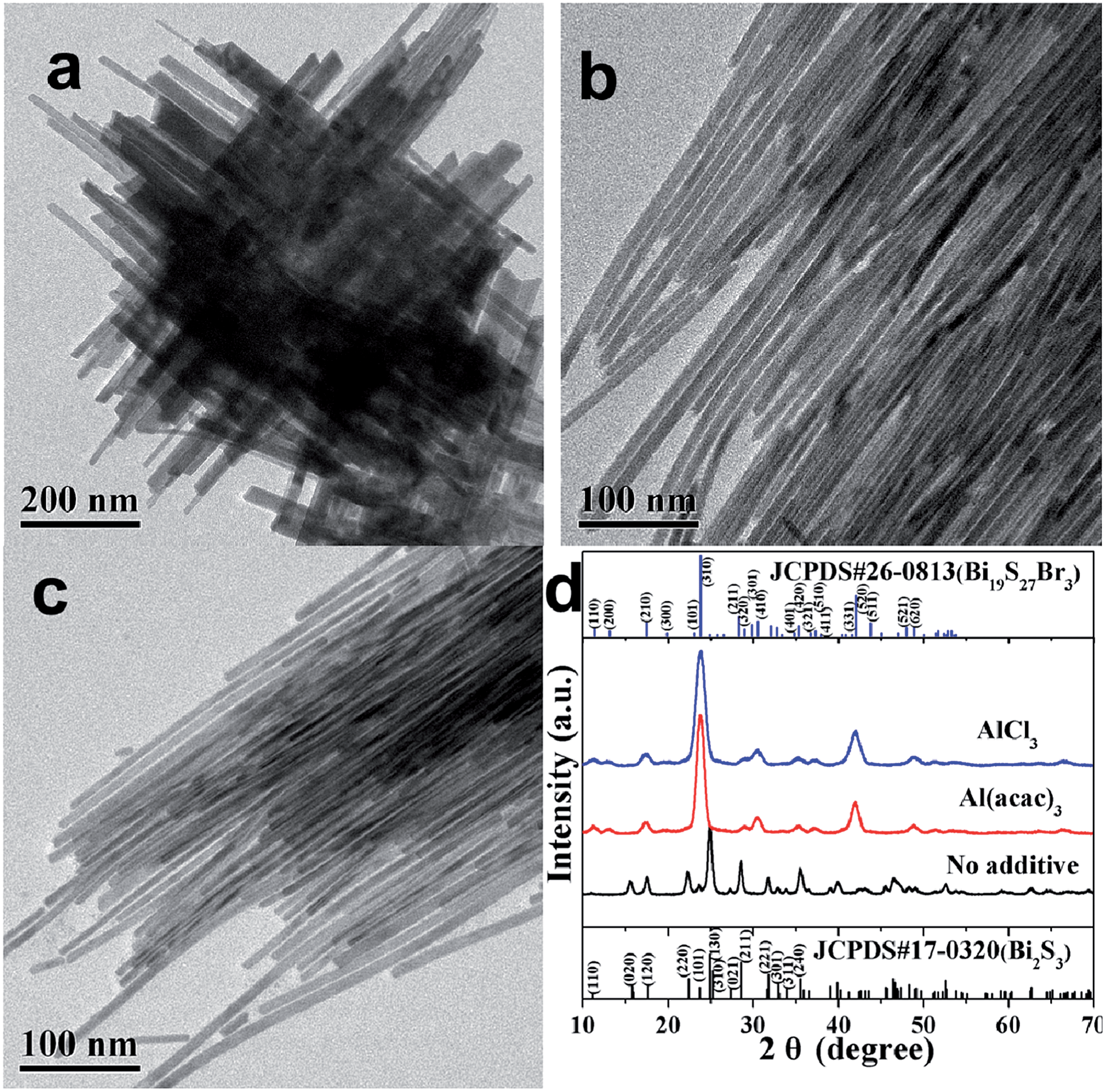
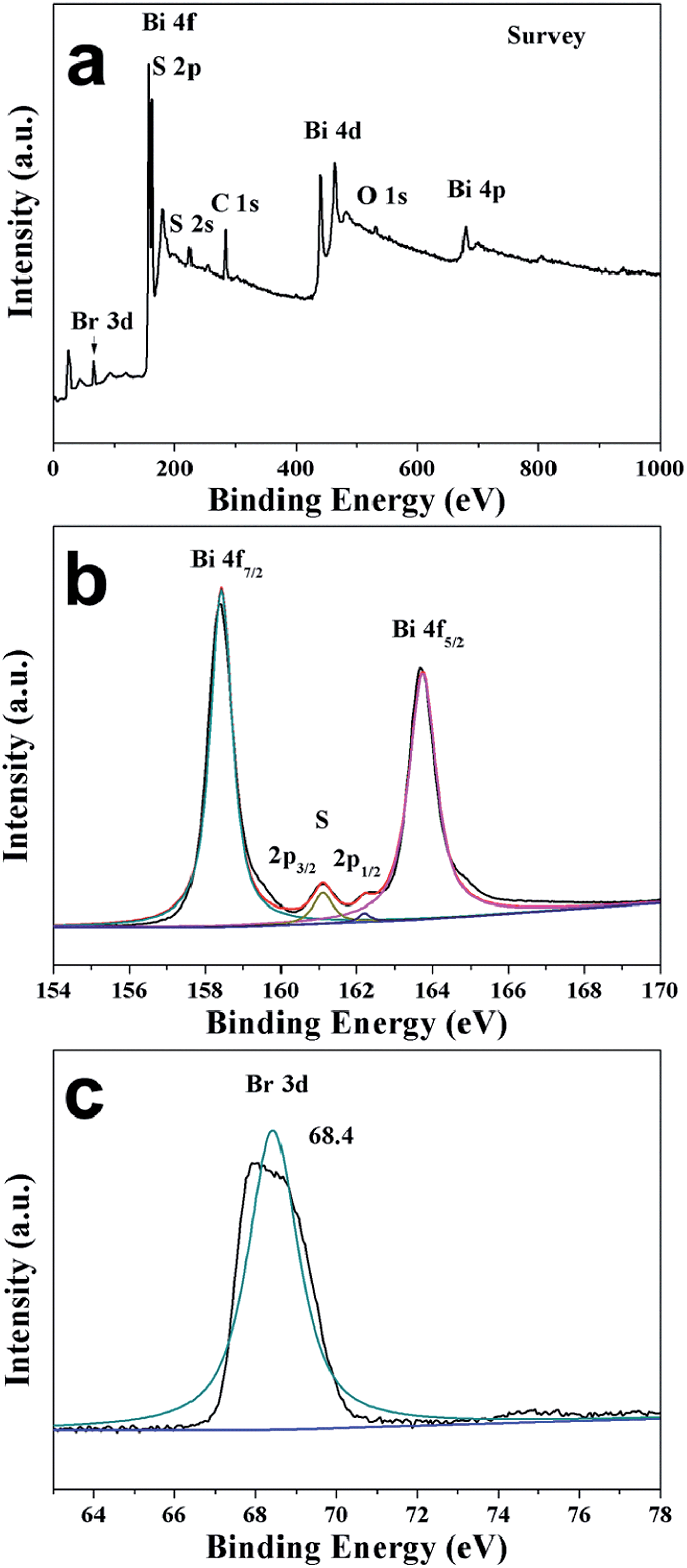
Fig. 1a shows the TEM image of the sample prepared in the absence of Al3+. The product was assembled from fabric-like NWs with a wide range of diameters, and was revealed to be orthorhombic Bi2S3 (JCPDS no. 17-0320) by XRD (Fig. 1d). The high-angle annular dark-field-scanning transmission microscopy (HAADF-STEM) and TEM image reveals the fabric-like morphology of Bi2S3 should be formed via physical crossover of non-uniform NWs (Fig. S1, ESI†). High resolution TEM (HRTEM) images along with the corresponding fast Fourier transform (FFT) pattern confirm the single crystalline nature of the product (Fig. S1, ESI†). Very interestingly, the presence of Al(acac)3 in the synthesis medium resulted in hexagonal-structured Bi19S27Br3 NWs (JCPDS no. 26-0813) with mean diameters of ∼9.0 nm, as shown in Fig. 1b (TEM) and Fig. 1d (XRD). It is noteworthy that the length of the as-synthesized Bi19S27Br3 NWs can be tuned in the range of 0.15–2 μm by varying the reaction duration while the mean diameters do not appear to change (Fig. S2, ESI,† the reaction temperature was kept at 180 °C). Moreover, the mean diameters can be tuned from ∼6.9 nm to ∼12 nm by varying the reaction temperature while the length of the NWs remain basically unchanged (Fig. S3, ESI,† the reaction time was kept at 30 min). Therefore, the presence of Al(acac)3 was critical for the formation of Bi19S27Br3 NWs and the reaction conditions were important to produce NWs with narrow size distributions. To ascertain whether it is the Al3+ that plays the key role in the formation of the well-defined Bi19S27Br3 NWs, AlCl3 was used as additive to replace Al(acac)3 in the synthesis process. Hexagonal Bi19S27Br3 NWs with very similar morphologies were again obtained (Fig. 1c and d), as in the case of Al(acac)3. Therefore, Al3+ ions can achieve not only morphological control, but also species transformation, i.e., from Bi2S3 to Bi19S27Br3 in this case. To investigate the NW composition, energy dispersive X-ray spectroscopy (EDS) was performed (Table S1, ESI†), showing the ratio of Bi![[thin space (1/6-em)]](https://www.rsc.org/images/entities/char_2009.gif) :S:Br was approximately 19:26:5. Thus the as-synthesized NWs are slightly sulfur poor and bromine rich. However, EDS cannot detect the presence of any Al element in the NWs. X-ray photoelectron spectroscopy (XPS) was further employed to characterize the Bi19S27Br3 NWs (Fig. 2), displaying peaks centred at 158.4 eV and 163.7 eV, which corresponded to the Bi 4f7/2 and Bi 4f5/2 of the Bi3+ ions,22 respectively. The peaks centred at 161.1 eV and 162.2 eV overlapping with Bi 4f were assigned to S 2p3/2 and S 2p1/2 of the S2− ions,22b,23 respectively. The signal with binding energy of 68.4 eV is characteristic of Br− ions (Br 3d). Altogether, the above data confirm that the Bi19S27Br3 NWs obtained through our colloidal approach are phase pure.
:S:Br was approximately 19:26:5. Thus the as-synthesized NWs are slightly sulfur poor and bromine rich. However, EDS cannot detect the presence of any Al element in the NWs. X-ray photoelectron spectroscopy (XPS) was further employed to characterize the Bi19S27Br3 NWs (Fig. 2), displaying peaks centred at 158.4 eV and 163.7 eV, which corresponded to the Bi 4f7/2 and Bi 4f5/2 of the Bi3+ ions,22 respectively. The peaks centred at 161.1 eV and 162.2 eV overlapping with Bi 4f were assigned to S 2p3/2 and S 2p1/2 of the S2− ions,22b,23 respectively. The signal with binding energy of 68.4 eV is characteristic of Br− ions (Br 3d). Altogether, the above data confirm that the Bi19S27Br3 NWs obtained through our colloidal approach are phase pure.
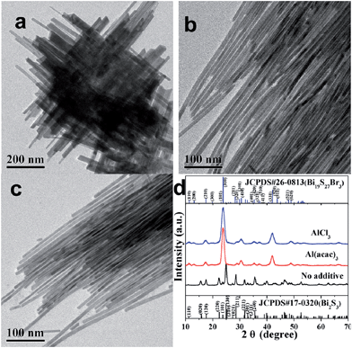 |
| | Fig. 1 TEM images of the as-synthesized NWs obtained by adding different salts into the reaction mixtures: (a) no additive, (b) Al(acac)3, (c) AlCl3, and (d) the corresponding XRD patterns of the three materials. | |
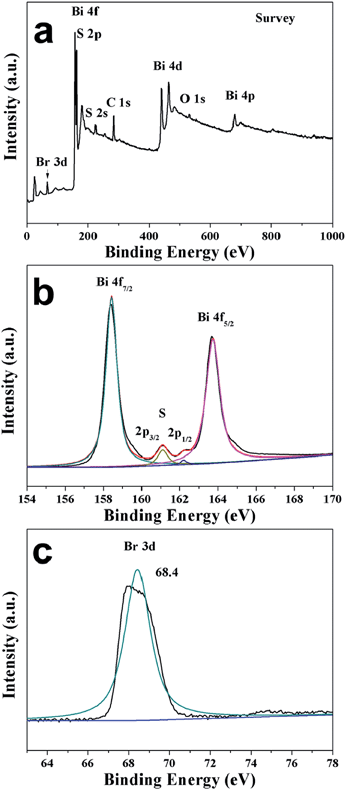 |
| | Fig. 2 XPS spectra of Bi19S27Br3 NWs: (a) survey XPS spectrum, (b) high-resolution spectra of Bi 4f and S 2p, and (c) high-resolution spectrum of Br 3d. | |
The influence of the concentration of Al3+ ions on the dimension of the resulting Bi19S27Br3 NWs was further studied by adding different amounts of Al3+ ions in the synthesis. It was found that the length of the Bi19S27Br3 NWs gradually decreased to a certain degree upon increasing the dosage of Al3+ ions, while the mean diameters of the Bi19S27Br3 NWs remained constant (Fig. S4, ESI†). The role of Al3+ ions in the shape control of the Bi19S27Br3 NWs is probably to promote crystal growth in a specific direction;18b the corresponding growth mechanisms of the NWs are shown in Scheme 1. If more Al3+ ions are present in the reaction mixture, the Bi precursors are divided into more regions, and more nucleation sites will be generated, resulting in the formation of shorter NWs. However, the transformation mechanism from Bi2S3 to Bi19S27Br3 needs to be elucidated in this study. It is proposed that Al3+ competes with Bi3+ in adsorbing S2− in the reaction system, which reduces the reaction probability between Bi3+ and S2−, leading to an incomplete replacement of Br− by S2−, thus forming the hexagonal-structured Bi19S27Br3. Another possible explanation is that, during the NW synthesis, BiBr3 and Al(acac)3 simultaneously dissolve in the ODE solution, where they should exist in molecular form. BiBr3 molecules may be surrounded by some Al3+via the electrostatic force between Br− and Al3+. In such a case, Al3+ can form a screen to suppress, to a certain degree, the attack of S2− to BiBr3, thus a portion of Br− is retained as a reaction intermediate, leading to the formation of a new species Bi19S27Br3. Deep understanding of the growth process is very complicated and further study should be performed with the aid of theoretical calculations. If any of the above explanations are true, it could be expected that other cations should also exert a similar influence on the reaction of nanowire growth in this study. Hence we chose Fe3+, Fe2+, Co3+, Co2+, and Ni2+ ions to investigate the influence of foreign metal ions on this reaction. Indeed, these cations function almost the same as Al3+ ions in the formation of Bi19S27Br3. The corresponding TEM images and XRD patterns for these nanowires are shown in Fig. S5 and S6, ESI,† respectively.
 |
| | Scheme 1 Schematic illustration for the proposed formation process of Bi19S27Br3 nanowires (OLA: oleylamine, OA: oleic acid, ODE: 1-octadecene). | |
To expand the present synthesis of Bi19S27Br3 NWs to other BiIIIVIAVIIA materials, we further prepared Bi19S27(Br3−x,Ix) (0 ≤ x ≤ 3) alloyed NWs. Fig. 3a presents the XRD patterns of the as-synthesized Bi19S27(Br3−x,Ix) NWs (0 ≤ x ≤ 3). For Bi19S27I3, the XRD pattern does not match any existing patterns in the standard JCPDS database, thus a diffraction pattern for hexagonal Bi19S27I3 was simulated on the basis of Bi19S27Br3 crystal structure by substituting the Br− lattice positions with I− (Table S2, ESI†). The lattice constants calculated from the experimental diffraction pattern (a = 15.65 Å and c = 4.026 Å) were used in this simulation. The d-spacings of the experimental reflections match well with the simulated ones, indicating that Bi19S27I3 NWs should exhibit the same hexagonal structure as Bi19S27Br3 NWs. Additionally, the major diffraction peaks shift systematically towards lower angles as the content of I increases, meaning that the larger I atoms have gradually replaced the smaller Br atoms in the lattices of the resulting NWs. More importantly, no additional peaks or peak splitting can be detected by XRD, ruling out the possibility of phase separation or separation nucleation that often occurs in the preparation of alloyed nanocrystals.21b Vegard's graph (Fig. 3b), obtained by plotting the lattice parameter values (a and c) versus composition, shows a near-linear trend with increasing iodide content, confirming the formation of a solid solution. Raman spectroscopy is a sensitive tool that reflects the phase purity of a material. The Raman spectra of the as-prepared NWs in Fig. S7, ESI† show five peaks, located at 127, 145, 192, 217 and 270 cm−1. The strongest Raman peak at ∼270 cm−1 can be assigned to the motion between the Bi and S atoms as well as the Br atom at rest for the Bi19S27Br3 NW. The absence of any Bi2S3 signals24 around 185, 236 and 260 cm−1 and any BiBr3 peaks25 around 143, 156 and 173 cm−1 confirmed the high purity of the Bi19S27Br3 NWs obtained in this study. Similar scenarios were observed for the other three samples with varied I/Br ratios. Therefore, we have successfully synthesized pure phase Bi19S27(Br3−x,Ix) NWs with chemical compositions can be consecutively tailored across the entire composition range (0 ≤ x ≤ 3).
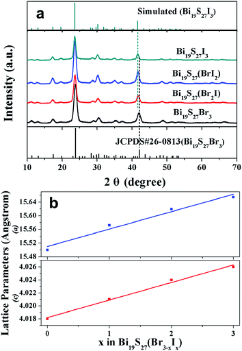 |
| | Fig. 3 XRD patterns (a) and Vegard's plot (b) of Bi19S27(Br3−x,Ix) with various I/(Br + I) ratios (0 ≤ x ≤ 3). | |
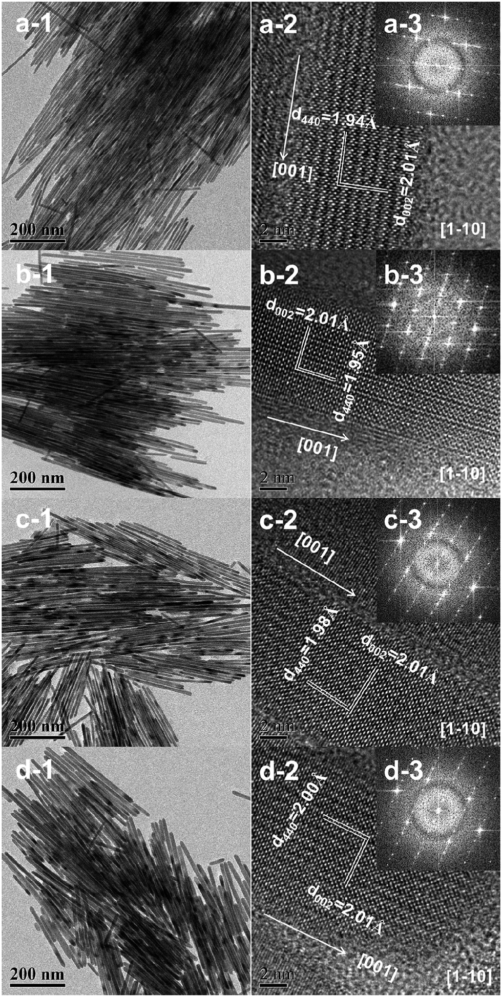
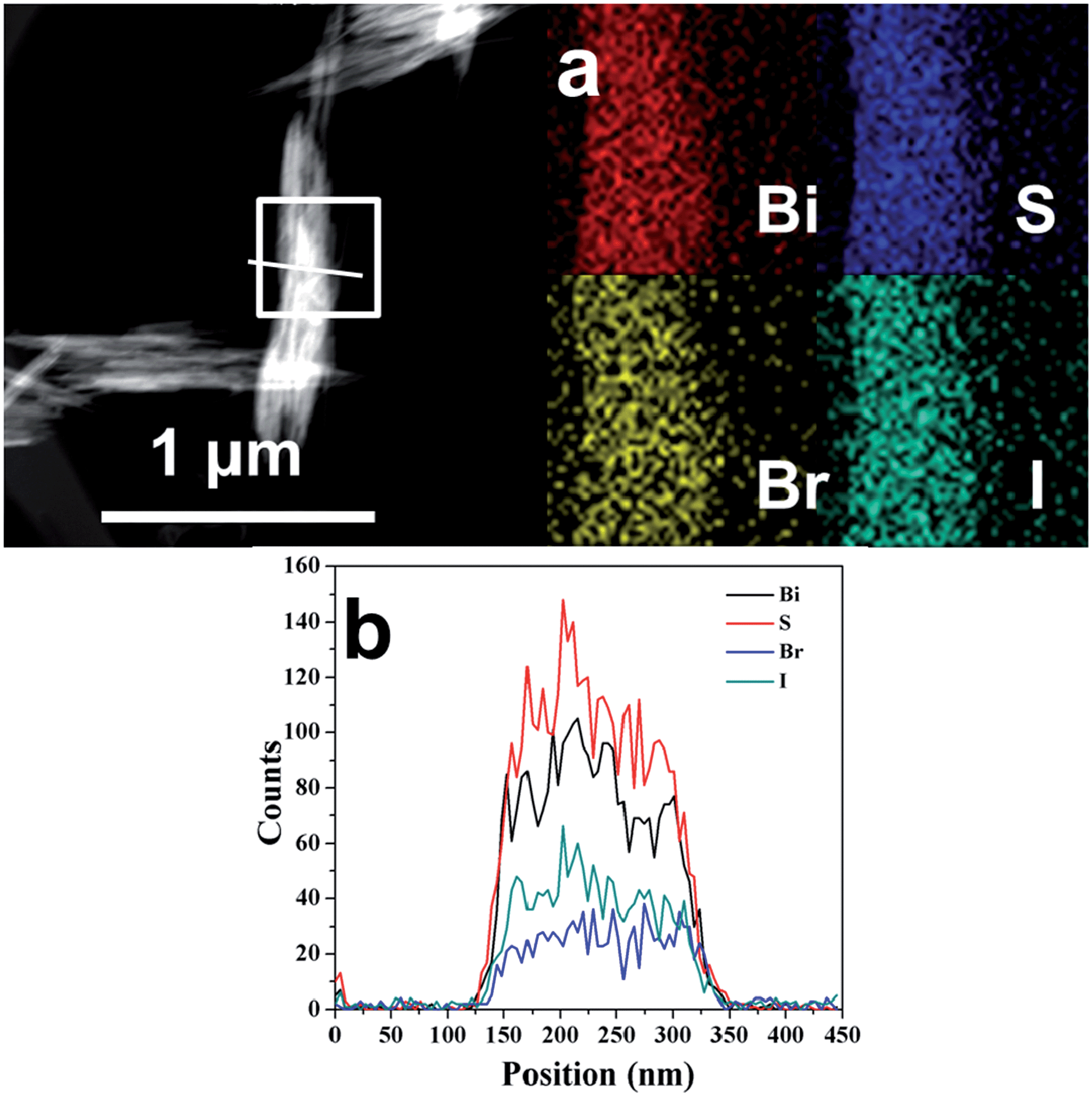
TEM and SEM were then performed to reveal the morphology and microstructures of the Bi19S27(Br3−x,Ix) alloyed NWs, as shown in Fig. 4 and S8, ESI,† respectively. The low-magnification TEM and SEM images display uniform diameter distributions of the Bi19S27(Br3−x,Ix) NWs, and the diameters increase gradually from ∼9.0 to ∼13.9 nm with as the I content increases (Fig. S9, ESI†). It is well-known that, to decrease the system energy, facets with lower energy will gradually grow larger, while the facets with higher energy gradually get smaller and even disappear during crystal growth. To gain insight into the variation in the diameters of the Bi19S27(Br3−x,Ix) NWs in this study, theoretical evaluation of the surface energies of the NW facets was carried out. The diameters of the hexagonal Bi19S27(Br3−x,Ix) NWs should be influenced significantly by the relative surface energies of the (110) facet/(001) facet. This is estimated to be 2.34 for the Bi19S27I3 NWs, which is significantly higher than the 0.71 for the Bi19S27Br3 NWs. This means that, in comparison with the Bi19S27Br3 NWs, the Bi19S27I3 NWs with larger (001) facets exhibit lower system energy. The (001) facet of the Bi19S27I3 would grow larger while the (110) facet becomes smaller. Therefore, the diameters of the Bi19S27(Br3−x,Ix) NWs increase gradually when the I content is increased. High-resolution TEM (HRTEM) images show that all the Bi19S27(Br3−x,Ix) NWs are highly crystalline with continuous lattice fringes and the corresponding fast Fourier transform (FFT) pattern of a single NW confirm their single crystalline nature. The lattice distance of 0.201 nm matches well with the (002) plane of the hexagonal Bi19S27Br3, indicating that the growth of the NWs is oriented along the [001] direction. Moreover, the interplanar crystal spacing of d440 increases from 0.194 nm to 0.200 nm with increasing I content, meaning again that the larger I atoms have successfully replaced the smaller Br atoms in the lattices of the resulting NWs, which is in good agreement with the XRD results. Elemental analysis by EDS (Table S1 and Fig. S10, ESI†) shows that an increase in the I content was accompanied by a decrease in the Br content in the range of 0 ≤ x ≤ 3 for the as-prepared Bi19S27(Br3−x,Ix) NWs. Moreover, elemental mapping and a line scan (Fig. 5) of the Bi19S27(BrI2) NWs confirm the homogeneous distribution of the four elements present. These results demonstrate the formation of alloyed NWs with a homogeneous distribution of Br and I in the Bi19S27(Br3−x,Ix) matrix.
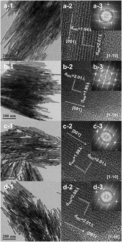 |
| | Fig. 4 TEM analysis of the Bi19S27(Br3−x,Ix) (0 ≤ x ≤ 3) NWs. (a)–(d) Denote respectively the Bi19S27Br3, Bi19S27(Br2I), Bi19S27(BrI2), and Bi19S27I3 NWs. 1, 2, and 3 represent the corresponding low magnification TEM images, HRTEM images and corresponding FFT patterns for these samples, respectively. | |
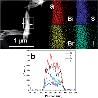 |
| | Fig. 5 HAADF-STEM image and corresponding EDS elemental mapping (a) and STEM-EDS line scan (b) of the Bi19S27(BrI2) NWs. | |
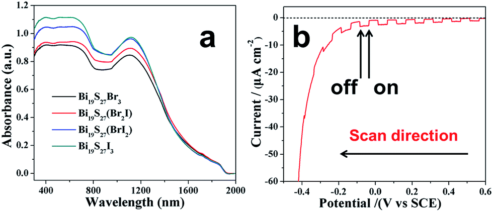
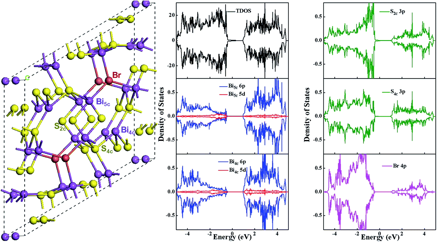
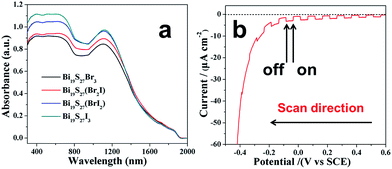
The UV-vis-NIR diffuse-reflectance spectroscopy (DRS) spectra of the Bi19S27(Br3−x,Ix) NWs (0 ≤ x ≤ 3) were measured to study their optical properties (Fig. 6a). A continuous strong absorption spanning the whole visible to near IR spectrum was found. It is noteworthy that the absorption intensity increases gradually as the I content increases. Tauc plots (Fig. S11, ESI†) were derived to determine the optical band gaps with the relationship of α2 plotted against the energy revealing that the Bi19S27Br3 NWs have a direct band gap of 0.815 eV. Interestingly, the band gap energies were basically unchanged upon varying the ratio of I/Br for the Bi19S27(Br3−x,Ix) NWs (0 ≤ x ≤ 3), meaning that the synthesized NWs exhibited band gaps independent of the composition, which is very different from the widely accepted Vegard's law for multi-component alloyed semiconductors.21 In order to deeply understand the electronic structure of Bi19S27Br3, density functional theory calculations were performed with the Vienna ab initio simulation package26 and a projector augmented wave method.27 The generalized gradient approximation (GGA) with the spin polarized Perdew–Burke–Ernzerhof (PBE) functional28 was used to relax the structure and compute the density of states. The results in Fig. 7 and S12, ESI,† show that the valence band maximum of Bi19S27Br3 and Bi19S27I3 is mostly composed of S 3p states and that the conduction band minimum mainly consists of Bi 6p states, slightly mixed with S 3p orbitals. In contrast, Br 4p or I 5p orbitals make important contributions to the lower region of the valence band (lower than −0.4 eV), which is possibly why the replacement of Br with I does not change the band gap of the as-synthesized NWs. The calculated band gap (about 0.6 eV) is smaller than our experimental value (around 0.82 eV) which may be due to shortcomings of the GGA method in underestimating the band gap.
 |
| | Fig. 6 (a) UV-vis-NIR diffuse-reflectance spectra (DRS) of the Bi19S27(Br3−x,Ix) (0 ≤ x ≤ 3) NWs, (b) transient photocurrent response of the Bi19S27(Br2I) NWs. | |
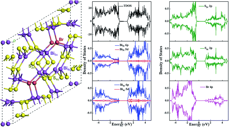 |
| | Fig. 7 The structural model and DOS for Bi19S27Br3. | |
We also investigated the photoelectrochemical (PEC) properties of the Bi19S27(Br3−x,Ix) NWs (0 ≤ x ≤ 3) by measuring the transient photocurrents of the NW films on fluorine tin oxide (FTO) in a photoelectrochemical cell. The photocurrent obtained from a Bi19S27(Br2I) NW electrode was negative (cathode current) (Fig. 6b), indicating that the as-synthesized NWs exhibit p-type semiconductor behavior.29 A constant bias experiment enables a more realistic evaluation of the charge transport dynamics for device applications. We hence carried out such a measurement. As shown in Fig. S13, ESI,† the photocurrents of the Bi19S27(Br3−x,Ix) NW films increased rapidly upon receiving illumination, and dropped immediately to their pre-illumination values without apparent degradation over many light on/off cycles. It can also be seen that the photocurrents increased gradually with increasing content of I, which may be due to the enhanced absorption intensities, as shown in Fig. 6a. Therefore, the Bi19S27(Br3−x,Ix) NWs (0 ≤ x ≤ 3) are sensitive to light illumination and are stable under experimental conditions, which is vital for device applications.
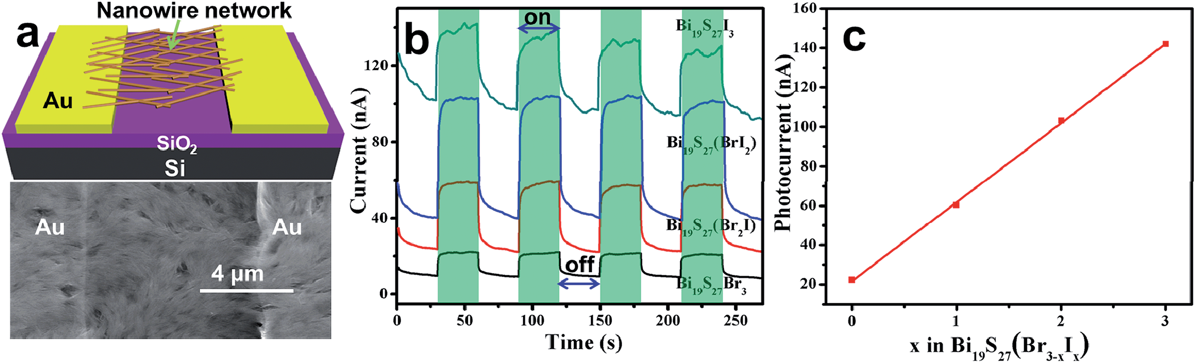
The combination of a strong absorption ability in the visible to near IR region of the spectrum and a sensitive response to light illumination makes the Bi19S27(Br3−x,Ix) NWs (0 ≤ x ≤ 3) excellent candidates for photodetectors (PDs). The as-synthesized alloyed NWs were directly drop-casted on a pre-prepared Au electrode (50 nm) paired onto a SiO2 (300 nm)/p+-Si substrate. Fig. 8a shows this as a schematic illustration and also a representative SEM image of the PD based on the NW network. Despite the short length and small diameter of the NWs, the NWs in the network can connect successfully both to each other and across the electrode pairs. Current versus voltage (I–V) curves of the four kinds of PDs measured in the dark are plotted in Fig. S14, ESI.† The linear shape of the curves demonstrates the ohmic contact of the NW networks with the Au electrodes. Significantly, under white light illumination (60 mW cm−2), all the devices show pronounced photoresponses (Fig. 8b), and the devices could be reversibly switched between low- and high-conduction states when the light was switched off and on repeatedly, revealing the high stability and reproducibility of the PDs. Close investigation of the on/off curves reveals that the highest photocurrent for the PDs increases with increasing iodide content (Fig. 8c), which is in good agreement with the PEC measurements. These results confirm the good optoelectronic properties of our NWs.
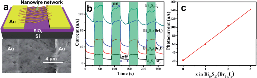 |
| | Fig. 8 (a) Schematic illustration of the PDs based on Bi19S27(Br3−x,Ix) NW networks (x = 0, 1, 2, 3). SEM image of a typical device is shown below. (b) Transient photoresponse of the PDs to pulsed incident light at a bias of +5 V. (c) Photocurrent versus iodide content (x) curve. | |
Conclusions
In summary, we have developed a facile solution-based method for the synthesis of highly uniform single-crystalline Bi19S27(Br3−x,Ix) alloyed NWs across the whole composition range (0 ≤ x ≤ 3) with the aid of foreign metal ions (Al3+). A systematic increase in the lattice constant values upon substitution of I− for Br− in Bi19S27Br3 confirms the formation of Bi19S27(Br3−x,Ix) alloyed NWs. The as-synthesized NWs show an unusual composition-independent band gap of ∼0.82 eV which is mainly due to the small contributions of the halogens to the valence band maximum and conduction band minimum. Photoelectrochemical measurements reveal that the Bi19S27(Br3−x,Ix) NWs are p-type semiconductors and sensitive to light irradiation. Moreover, PDs made of these NWs exhibit high sensitivity to white light, confirming the great potential of Bi19S27(Br3−x,Ix) NWs in high-performance optoelectronic devices.
Acknowledgements
We acknowledge the financial support from the National Basic Research Program of China (no. 2013CB933500, 2012CB932400), the Natural Science Foundation of China (no. 21322202 and 20873141) and the “Hundred Talents Program” of the Chinese Academy of Sciences.
Notes and references
-
(a) N. P. Dasgupta, J. Sun, C. Liu, S. Brittman, S. C. Andrews, J. Lim, H. Gao, R. Yan and P. Yang, Adv. Mater., 2014, 26, 2137 CrossRef CAS PubMed;
(b) A. I. Hochbaum and P. Yang, Chem. Rev., 2010, 110, 527 CrossRef CAS PubMed.
- F. Qian, S. Gradečak, Y. Li, C.-Y. Wen and C. M. Lieber, Nano Lett., 2005, 5, 2287 CrossRef CAS PubMed.
-
(a) T. J. Kempa, R. W. Day, S.-K. Kim, H.-G. Park and C. M. Lieber, Energy Environ. Sci., 2013, 6, 719 RSC;
(b) S. Liu, X. Guo, M. Li, W.-H. Zhang, X. Liu and C. Li, Angew. Chem., Int. Ed., 2011, 50, 12050 CrossRef CAS PubMed.
-
(a) J. Miao, W. Hu, N. Guo, Z. Lu, X. Zou, L. Liao, S. Shi, P. Chen, Z. Fan, J. C. Ho, T.-X. Li, X. S. Chen and W. Lu, ACS Nano, 2014, 8, 3628 CrossRef CAS PubMed;
(b) G. Chen, B. Liang, X. Liu, Z. Liu, G. Yu, X. Xie, T. Luo, D. Chen, M. Zhu, G. Shen and Z. Fan, ACS Nano, 2014, 8, 787 CrossRef CAS PubMed;
(c) J.-J. Wang, Y.-Q. Wang, F.-F. Cao, Y.-G. Guo and L.-J. Wan, J. Am. Chem. Soc., 2010, 132, 12218 CrossRef CAS PubMed.
- L. Li, H. Lu, Z. Yang, L. Tong, Y. Bando and D. Golberg, Adv. Mater., 2013, 25, 1109 CrossRef CAS PubMed.
- H. Fang, T. Feng, H. Yang, X. Ruan and Y. Wu, Nano Lett., 2013, 13, 2058 CrossRef CAS PubMed.
- E. W. Wong, P. E. Sheehan and C. M. Lieber, Science, 1997, 277, 1971 CrossRef CAS.
- Y. Xia, P. Yang, Y. Sun, Y. Wu, B. Mayers, B. Gates, Y. Yin, F. Kim and H. Yan, Adv. Mater., 2003, 15, 353 CrossRef CAS PubMed.
-
(a) G. Meng, T. Yanagida, K. Nagashima, H. Yoshida, M. Kanai, A. Klamchuen, F. Zhuge, Y. He, S. Rahong, X. Fang, S. Takeda and T. Kawai, J. Am. Chem. Soc., 2013, 135, 7033 CrossRef CAS PubMed;
(b) M. Heurlin, M. H. Magnusson, D. Lindgren, M. Ek, L. R. Wallenberg, K. Deppert and L. Samuelson, Nature, 2012, 492, 90 CrossRef CAS PubMed;
(c) H.-Y. Tuan, D. C. Lee and B. A. Korgel, Angew. Chem., Int. Ed., 2006, 45, 5184 CrossRef CAS PubMed.
-
(a) J. Joo, B. Y. Chow, M. Prakash, E. S. Boyden and J. M. Jacobson, Nat. Mater., 2011, 10, 596 CrossRef CAS PubMed;
(b) F. Meng, S. A. Morin and S. Jin, J. Am. Chem. Soc., 2011, 133, 8408 CrossRef CAS PubMed.
-
(a) C. Wang, Y. Hu, C. M. Lieber and S. Sun, J. Am. Chem. Soc., 2008, 130, 8902 CrossRef CAS PubMed;
(b) J. Tang, Z. Huo, S. Brittman, H. Gao and P. Yang, Nat. Nanotechnol., 2011, 6, 568 CrossRef CAS PubMed.
-
(a) C. O'Sullivan, R. D. Gunning, A. Sanyal, C. A. Barrett, H. Geaney, F. R. Laffir, S. Ahmed and K. M. Ryan, J. Am. Chem. Soc., 2009, 131, 12250 CrossRef PubMed;
(b) N. Pradhan, H. Xu and X. Peng, Nano Lett., 2006, 6, 720 CrossRef CAS PubMed;
(c) K.-S. Cho, D. V. Talapin, W. Gaschler and C. B. Murray, J. Am. Chem. Soc., 2005, 127, 7140 CrossRef CAS PubMed.
-
(a) X. Zhang, N. Bao, K. Ramasamy, Y.-H. A. Wang, Y. Wang, B. Lin and A. Gupta, Chem. Commun., 2012, 48, 4956 RSC;
(b) Y. Zou, X. Su and J. Jiang, J. Am. Chem. Soc., 2013, 135, 18377 CrossRef CAS PubMed;
(c) M. E. Norako, M. J. Greaney and R. L. Brutchey, J. Am. Chem. Soc., 2012, 134, 23 CrossRef CAS PubMed.
-
(a) K. P. Rice, A. E. Saunders and M. P. Stoykovich, J. Am. Chem. Soc., 2013, 135, 6669 CrossRef CAS PubMed;
(b) Y.-H. A. Wang, X. Zhang, N. Bao, B. Lin and A. Gupta, J. Am. Chem. Soc., 2011, 133, 11072 CrossRef CAS PubMed;
(c) X. Peng, L. Manna, W. Yang, J. Wickham, E. Scher, A. Kadavanich and A. P. Alivisatos, Nature, 2000, 404, 59 CrossRef CAS PubMed;
(d) W. Zhou, M. Yao, L. Guo, Y. Li, J. Li and S. Yang, J. Am. Chem. Soc., 2009, 131, 2959 CrossRef CAS PubMed;
(e) J. Nai, Y. Tian, X. Guan and L. Guo, J. Am. Chem. Soc., 2013, 135, 16082 CrossRef CAS PubMed.
-
(a) C. Yang, B. Zhou, S. Miao, C. Yang, B. Cai, W.-H. Zhang and X. Xu, J. Am. Chem. Soc., 2013, 135, 5958 CrossRef CAS PubMed;
(b) A. Singh, S. Singh, S. Levcenko, T. Unold, F. Laffir and K. M. Ryan, Angew. Chem., Int. Ed., 2013, 52, 9120 CrossRef CAS PubMed;
(c) Y. Wu, B. Zhou, M. Li, C. Yang, W.-H. Zhang and C. Li, Chem. Commun., 2014, 50, 12738 RSC.
-
(a) L. Wu, B. Quan, Y. Liu, R. Song and Z. Tang, ACS Nano, 2011, 5, 2224 CrossRef CAS PubMed;
(b) W. Han, L. Yi, N. Zhao, A. Tang, M. Gao and Z. Tang, J. Am. Chem. Soc., 2008, 130, 13152 CrossRef CAS PubMed.
-
(a) J.-j. Wang, P. Liu, C. C. Seaton and K. M. Ryan, J. Am. Chem. Soc., 2014, 136, 7954 CrossRef CAS PubMed;
(b) Z. Li and X. Peng, J. Am. Chem. Soc., 2011, 133, 6578 CrossRef CAS PubMed;
(c) E. A. Weiss, Acc. Chem. Res., 2013, 46, 2607 CrossRef CAS PubMed.
-
(a) W. Li, R. Zamani, P. Rivera Gil, B. Pelaz, M. Ibáñez, D. Cadavid, A. Shavel, R. A. Alvarez-Puebla, W. J. Parak, J. Arbiol and A. Cabot, J. Am. Chem. Soc., 2013, 135, 7098 CrossRef CAS PubMed;
(b) W. Li, R. Zamani, M. Ibáñez, D. Cadavid, A. Shavel, J. R. Morante, J. Arbiol and A. Cabot, J. Am. Chem. Soc., 2013, 135, 4664 CrossRef CAS PubMed.
-
(a) Y. Wu, B. Yuan, M. Li, W.-H. Zhang, Y. Liu and C. Li, Chem. Sci., 2015, 6, 1873 RSC;
(b) V. Krämer, J. Appl. Crystallogr., 1973, 6, 499 CrossRef;
(c) L. Zhu, Y. Xie, X. Zheng, X. Yin and X. Tian, Inorg. Chem., 2002, 41, 4560 CrossRef CAS PubMed;
(d) C. Deng, H. Guan and X. Tian, Mater. Lett., 2013, 108, 17 CrossRef CAS PubMed.
- K. Mariolacos, Mater. Res. Bull., 2004, 39, 591 CrossRef CAS PubMed.
-
(a) L. Vegard and H. Schjelderup, Z. Phys., 1917, 18, 93 CAS;
(b) M. D. Regulacio and M.-Y. Han, Acc. Chem. Res., 2010, 43, 621 CrossRef CAS PubMed.
-
(a) K. Ai, Y. Liu, J. Liu, Q. Yuan, Y. He and L. Lu, Adv. Mater., 2011, 23, 4886 CrossRef CAS PubMed;
(b) J. Grigas, E. Talik and V. Lazauskas, Phys. Status Solidi B, 2002, 232, 220 CrossRef CAS.
- H. Li, Q. Zhang, A. Pan, Y. Wang, B. Zou and H. J. Fan, Chem. Mater., 2011, 23, 1299 CrossRef CAS.
- Y. Zhao, K. T. E. Chua, C. K. Gan, J. Zhang, B. Peng, Z. Peng and Q. Xiong, Phys. Rev. B: Condens. Matter Mater. Phys., 2011, 84, 205330 CrossRef.
- G. A. Bowmaker, J. M. Harrowfield, P. C. Junk, B. W. Shelton and A. H. White, Aust. J. Chem., 1998, 51, 285 CrossRef CAS.
-
(a) G. Kresse and J. Furthmüller, Comput. Mater. Sci., 1996, 6, 15 CrossRef CAS;
(b) G. Kresse and J. Furthmüller, Phys. Rev. B: Condens. Matter Mater. Phys., 1996, 54, 11169 CrossRef CAS.
-
(a) P. E. Blöchl, Phys. Rev. B: Condens. Matter Mater. Phys., 1994, 50, 17953 CrossRef;
(b) G. Kresse and D. Joubert, Phys. Rev. B: Condens. Matter Mater. Phys., 1999, 59, 1758 CrossRef CAS.
- J. P. Predew, K. Burke and M. Ernzerhof, Phys. Rev. Lett., 1996, 77, 3865 CrossRef.
- D. H. Webber and R. L. Brutchey, J. Am. Chem. Soc., 2012, 134, 1085 CrossRef CAS PubMed.
Footnote |
| † Electronic supplementary information (ESI) available: Experimental details, XRD patterns, TEM and HRTEM images, energy-dispersive X-ray spectra, UV-vis spectra, and Tauc plots. See DOI: 10.1039/c5sc00708a |
|
| This journal is © The Royal Society of Chemistry 2015 |
Click here to see how this site uses Cookies. View our privacy policy here. 
 Open Access Article
 This Open Access Article is licensed under a Creative Commons Attribution-Non Commercial 3.0 Unported Licence