An extremely superhydrophobic and intrinsically stable Si/fluorocarbon energetic composite based on upright nano/submicron-sized Si wire arrays

Xiang Zhou*a, Ying Zhub, Kaili Zhangb, Jian Lub and Wei Jianga
aNational Special Superfine Powder Engineering Research Center, Nanjing University of Science and Technology, Nanjing, China. E-mail: zhouxiang@njust.edu.cn
bDepartment of Mechanical and Biomedical Engineering, City University of Hong Kong, 83 Tat Chee Avenue, Kowloon, Hong Kong

Received 20th November 2015 , Accepted 7th December 2015

First published on 9th December 2015


Abstract

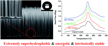
Si is chemically stable compared with many highly reactive metallic elements when used as a fuel for energetic formulations, and thus Si-based energetic composites can be intrinsically suitable for long-term storage. In this study upright nano/submicron-sized Si wire arrays are fabricated by a mask-free deep reactive ion etching method. A fluorocarbon layer is then sputter-deposited onto the Si wire arrays to form a Si/fluorocarbon energetic composite. The morphological and compositional information of the composites is characterized by various techniques such as scanning electron microscopy, X-ray photoelectron spectroscopy, Fourier transform infrared spectroscopy, and X-ray diffraction. The energetic property is studied by thermal analysis. Orderly Si wires are obtained by tuning the passivation/etching ratio in a processing cycle. As the total processing time increases, the number density of Si wires decreases while the length increases. The effects of power density and Ar flow rate on the chemical composition of the sputtered fluorocarbon are also investigated, but neither of them show appreciable impact within the ranges studied. The Si/fluorocarbon surface is so superhydrophobic that the water drops roll easily and the contact angles can hardly be measured. Si wires and fluorocarbon react exothermically and much gas products are generated. After a prolonged accelerated aging test, the Si/fluorocarbon energetic composites show almost no decay of the energy density. Si wire arrays can also be used as scaffolds to prepare other highly superhydrophobic energetic composites.


1. Introduction

Nanoenergetic materials show enhanced energetic capability compared to their micro and bulk counterpart, which mainly results from the unique interfacial characteristics and the reduced heat and mass diffusion restrictions.1–4 The potential applications of nanoenergetic materials are versatile, such as ignition and propulsion in the defence industry,5,6 initiators for air bags and belt-tensioners in the automobile industry,7,8 microfluidics actuation, molecular delivery, and biocidal effect in biomedicine,9–11 and materials synthesis and processing in materials science and engineering.12,13 More than two decades has passed since the advent of the idea. Among the numerous studies, some features are always the pursuits of researchers, such as the superior and controllable energetic capability, the cost-effective and environment-benign synthesis method, and the reliability of function and stability during storage. Up to now, most research work is concerned with the energetic capability, which is also the prime driving force of the development of nanoenergetic materials. Nano-sized metals, especially nano-Al, are mostly used as the fuels in the various energetic formulations. Highly reactive n-Al powder is susceptible to the environmental conditions like moisture-laden air.14 Because the particle size is in the nano-meter order, even a thin oxide/hydroxide shell will cause severe degradation to the energy density and affect the ignition and combustion characteristics.2 Si is not as reactive as many metals; on the other hand, Si can also react with some polymers with appreciable heats of reaction, e.g., Si can react with polytetrafluoroethylene (PTFE) with a calculated heat release more than 6 kJ g−1 according to eqn (1).15 Moreover, the reaction product is gaseous in standard conditions, which makes Si/PTFE advantageous to many other thermite formulations with less gas evolution. Therefore, Si can be used to prepare superior energetic composites which are intrinsically suitable for long-term storage.
 
Si + C2F4 (c) → SiF4 + 2C ΔHӨ = −6.21 kJ g−1 (1)

Actually, there are already many studies on Si-based nanoenergetic composites. The Si wafers were doped and crushed into powder, and then the effect of doping on the reaction and combustion characteristics of Si/PTFE was studied.16 Terry et al. systematically investigated the roles of specific surface area, active content, morphology, and particle size of the Si powder on the combustion behaviour of Si/PTFE/Viton nanoenergetic composites.17 However, powder-mixing technique was used in these studies to prepare nanoenergetic composites, and hence the interfacial contact and distribution of fuel and oxidizer are rather random. As one kind of nanostructured energetic composites, nano-porous Si-based nanoenergetics attract much more attention.4 As the oxidizer is embedded into the nano-pores of silicon, the intimate contact and homogeneous distribution of fuel and oxidizer are obtained. Nano-porous Si-based nanoenergetics show impressive energetic capability,18,19 but there are also many shortcomings, such as the safety concerns arising from the high sensitivity, the questionable storage stability due to the hygroscopic oxidizers used, and the green-chemistry issue caused by the use of hydrofluoric acid.7,20 Superhydrophobic/hydrophobic nanoenergetic materials have been reported in recent years, and the superhydrophobicity/hydrophobicity is very beneficial to the long-term storage stability of the nanoenergetic materials.21–23

In this study, upright nano/submicron-sized Si wire arrays are fabricated by a mask-free deep reactive ion etching (DRIE) method. Fluorocarbon is then sputtered onto the Si wires to form Si/fluorocarbon nanostructured energetic composite. The Si/fluorocarbon reacts exothermically with abundant gas evolution, and the Si/fluorocarbon arrays are extremely superhydrophobic. Si wire arrays can also be used as scaffolds to prepare other energetic composites such as Si/fluorocarbon/Al/fluorocarbon which are also exceptionally superhydrophobic.

2. Experimental section

2.1. Sample preparation

Upright Si wire arrays are fabricated by a mask-free DRIE method, also known as “black silicon” method. An inductively coupled plasma etcher (Surface Technology Systems Ltd) is used, and the procedure is adapted from that reported by Cho et al.24 First, a polished silicon wafer (4 inch in diameter and 500 μm in thickness) is immersed into a mixture of concentrated H2SO4 (98%) and H2O2 (30%) at 120 °C for 10 min (volumetric ratio 10[thin space (1/6-em)]:[thin space (1/6-em)]1). After dried in a rinser/dryer, the wafer is put into the etcher for processing. A passivation/etching cycle is set as 4 s/6 s or 6 s/6 s. In the passivation half-cycle, C4F8 flows at 85 sccm. In the etching half-cycle, SF6 and O2 flow at 130 sccm and 13 sccm, respectively. Coil power and platen power are 600 W and 30 W, respectively, for both the passivation and etching half-cycles. The total processing time is varied to get Si wires with different lengths and number densities.

Fluorocarbon thin film is prepared by sputtering PTFE target in a JunSun MGM-600 sputtering system. The target is 2 inch in diameter and 0.125 inch in thickness. The distance between the target and the substrate is 11 cm, and the included angle between the target surface normal and substrate surface is 60°. The substrate stage rotates at 10 rpm. Five combinations of sputtering power and Ar flow rate are used so as to study their effect on the property of the deposited fluorocarbon thin films. The combinations are as follows: 90 W/30 sccm, 120 W/30 sccm, 150 W/30 sccm, 120 W/20 sccm, and 120 W/40 sccm. The upper limit of power is 150 W for our machine. Sputtering power less than 90 W is not used because the deposition rate is too low.

Si/fluorocarbon energetic composite is prepared by depositing a layer of fluorocarbon with a certain thickness onto the Si wires. Si/fluorocarbon/Al/fluorocarbon is prepared by alternate sputter deposition of fluorocarbon and Al onto Si wires scaffolds. Individual fluorocarbon and Al layers are of thicknesses of 200 and 150 nm, respectively.

2.2. Morphological and compositional characterization

The fabricated Si wire arrays are observed by a field-emission scanning electron microscope (FESEM, FEI Quanta 450). Accelerating voltage is 5 kV, and no Au coating is used for imaging. X-ray photoelectron spectroscopy (XPS, Physical Electronics PHI5802) and Fourier transform infrared spectroscopy (FTIR, Bruker Tensor 27) are used to determine the composition of the sputter-deposited fluorocarbon thin films. XPS is also used to characterize the as-prepared Si wire arrays. The XPS measurement is conducted with a monochromatized Al Kα X-ray source (1486.6 eV). The chamber pressure is on the order of 10−9 Torr during tests. The photoelectron takeoff angle (with respect to the sample surface) is 45°. No Ar etching is used before characterization. The pass energies of the survey-scan and high-resolution C 1 s XPS measurements are 187.85 and 11.75 eV, respectively. The high-resolution spectrums are curve-fitted into several components by the software named XPS peak. During the curve fitting, the line width (full width at half maximum) of all the constituent peaks is kept constant. As to FTIR tests, fluorocarbon thin films are first deposited onto the KBr pellets. KBr pellets are prepared by pressing 100 mg powder with 60 kN force for 10 min. FTIR spectrum is collected by cumulating 16 scans at a resolution of 4 cm−1. X-ray diffraction (XRD, Bruker D2 Phaser) is used to determine the composition of the as-prepared Si/fluorocarbon energetic composite as well as the reaction product after thermal analysis. The XRD is performed at 30 kV using Cu Kα radiation (λ = 1.5418 Å).

2.3. Wettability test, accelerated aging test, and thermal analysis

KRÜSS DSA100 drop shape analysis system is used for the water drop contact angle test of the Si/fluorocarbon and Si/fluorocarbon/Al/fluorocarbon surfaces. A deionized water droplet of 10 μL is used each time. In order to explore the intrinsic stability of the Si/fluorocarbon, the samples are exposed to a highly humid atmosphere for extended duration. A temperature and humidity chamber (Welltech YTH-63) is used to simulate a constant high-humidity environment. The uniformities of temperature and relative humidity within the chamber are ±1 °C and ±5%, respectively. The samples are exposed to an environment of 95% relative humidity/40 °C 12 hours per day. The equipment is turned off at night, and the samples are left in the chamber overnight, with the chamber door closed. The temperature and relative humidity within the chamber are around 25 °C and >98%, respectively. The exposure conditions are very harsh compared with that of normal storage conditions in order to carry out accelerated aging test. The exothermic reactions of Si/fluorocarbon and Si/fluorocarbon/Al/fluorocarbon energetic composites are characterized by differential scanning calorimetry (DSC, TA Instruments Q20). The samples are scraped off the silicon wafer for testing. DSC analysis is conducted from 40 to 680 °C with a heating rate of 10 °C min−1 under 50 mL min−1 Ar flow. A second run is conducted for each test and then deducted from the first run in order to obtain a good baseline. As the exothermic reaction of Si/fluorocarbon also accompanies with gas evolution, thermo-gravimetric analysis (TA Instruments Q600) is conducted to provide more information about the reaction process. The sample is heated from 40 to 800 °C with a heating rate of 10 °C min−1 under 100 mL min−1 Ar flow. For all the tests, Ar flow is started 30 min before temperature ramp to replace as much as possible the air in the chamber. Universal analysis 2000 software is used to process the data.

3. Results

3.1. Morphology and composition of the nano/submicron-sized Si wire arrays

Fig. 1 shows the top-view (Fig. 1a, c, e and g) and cross-sectional (Fig. 1b, d, f and h) FESEM images of the Si wires obtained from 4 s/6 s passivation/etching cycles. The total processing time is 20, 30, 40, and 60 min, respectively, for the samples from the top to the bottom in the figure. As shown in the images, the length of Si wires increases with the processing time but the number density decreases. There seems to be a threshold of processing time below which no Si wires form, just as that shown in Fig. 1b when the processing time is 20 min. Similar results were also reported in the literature.24 The top of each Si wire is irregular with dimension in nanometer range, while the bulk of each Si wire has constant diameter in submicron range. The diameter does not show strong dependence on the processing time. It is also found that the Si wire arrays are not orderly. The length of individual Si wires varies and there are many fallen wires.
image file: c5ra24633d-f1.tif
Fig. 1 Top-view (a, c, e and g) and cross-sectional (b, d, f and h) FESEM images of Si wires obtained from 4 s/6 s passivation/etching cycles. The total processing time is 20 (a and b), 30 (c and d), 40 (e and f), and 60 min (g and h), respectively.

Fig. S1 shows the top-view and cross-sectional microscopic images of the Si/fluorocarbon/Al/fluorocarbon. The Si wires are obtained after 40 min of processing. The results show that the fluorocarbon and Al layers are coated along each Si wires uniformly.

Fig. 2 shows the top-view (Fig. 2a and b), 45° tilted view (Fig. 2c and d), and cross-sectional (Fig. 2e–h) FESEM images of Si wires obtained from 6 s/6 s passivation/etching cycles. The total processing time is 36 and 48 min, respectively. Therefore, the total etching time is 18 and 24 min, respectively, which are the same as those of 40 and 60 min processing time under 4 s/6 s passivation/etching cycles. Quite different from the results of 4 s/6 s passivation/etching cycles, the Si wire arrays are neat and orderly. The length of Si wires is very uniform and there are hardly fallen wires found. The top-view images can only show scattered dots while the wafer surface is invisible. Interestingly, although the total etching time is the same, the Si wire arrays show much higher number density and larger length than those from 4 s/6 s passivation/etching cycles. The average length of Si wires after 36 min processing time is 16 μm, and it further increases to 26 μm when the total processing time is 48 min. Fig. 2g and h shows the enlarged images of the top and the bulk of Si wires, respectively. There is a helix-like pattern in each Si wires, which is caused by the alternating passivation and etching processes.


image file: c5ra24633d-f2.tif
Fig. 2 Top-view (a and b), 45° tilted view (c and d), and cross-sectional (e–h) FESEM images of Si wires obtained from 6 s/6 s passivation/etching cycles. The total processing time is 36 (a, c, e, g and h) and 48 min (b, d and f), respectively.

Fig. 3 shows the XPS spectra of the Si wire arrays. The samples are from 36 min DRIE under 6 s/6 s passivation/etching cycles. C 1s, F 1s, and F KLL signals are obvious in the survey scan spectrum as shown in Fig. 3a, indicating that a thin fluorocarbon layer is coated around the Si wires. Fig. 3b shows a high-resolution spectrum of C 1s, which reveals that the fluorocarbon layer consists of CF2, CF, and CF3 functional groups. Fig. 3c shows a high-resolution spectrum of Si 2p, in which the chemical shift due to oxide is found.


image file: c5ra24633d-f3.tif
Fig. 3 (a) A survey scan spectrum of the Si wires and (b and c) high-resolution spectra of C 1s (b) and Si 2p (c).

The XRD pattern of the Si wire arrays is shown in Fig. 4. A very strong diffraction peak is observed to centre at about 69°, which is caused by the (400) lattice planes. The fabricated Si wires preserve the single-crystal nature of the wafer very well.


image file: c5ra24633d-f4.tif
Fig. 4 The XRD patterns of the Si wires, Si/fluorocarbon, and the reaction products of Si/fluorocarbon reclaimed from DSC test.

3.2. Molecular structure of the fluorocarbon thin film

Fig. 5 shows the high-resolution C 1s XPS spectra (Fig. 5a) and FTIR spectra (Fig. 5b) of the fluorocarbon thin films prepared under different combinations of power and Ar flow rate. Five samples show very similar C 1s XPS spectra. Five kinds of C species are found in each spectrum, which can be indexed to [C with combining low line]H (284.5 eV), [C with combining low line]–CFn (286.6 eV), [C with combining low line]F (289.1 eV), [C with combining low line]F2 (291.2 eV), and [C with combining low line]F3 (293.2 eV), respectively.23,25 The relative concentrations of the different C species and the corresponding F/C ratios are calculated and listed in Table 1. Considering the 10% accuracy of XPS for quantitative analysis, the results actually show no apparent difference. XPS is suitable for surface characterization, and therefore FTIR spectra are collected to show more information of the bulk of the materials. Five kinds of samples also show quite similar FTIR spectra. An absorption band which centres at 1221 cm−1 is most obvious, which is attributed to the symmetric stretching vibration of CF2 groups. Absorption peaks at 736 and 981 cm−1 correspond to the vibration of CF3 groups.25,26 A weak absorption peak at 537 cm−1 is caused by the wagging vibration of CF2 groups.25 An absorption band around 1717 cm−1 is indexed to the C[double bond, length as m-dash]C stretching vibrations.27
image file: c5ra24633d-f5.tif
Fig. 5 (a) High-resolution C 1s XPS spectra and (b) FTIR spectra of the fluorocarbon thin films prepared under different combinations of power and Ar flow rate.
Table 1 The relative concentrations of different C species and the corresponding F/C ratios of the fluorocarbon thin films sputter deposited under different combinations of power and Ar flow rate
Sample Concentration of C species (mol%) F/C ratio
[C with combining low line]F3 [C with combining low line]F2 [C with combining low line]F [C with combining low line]–CFn [C with combining low line]H
150 W, 30 sccm 10.4 43.2 23.0 20.9 2.5 1.46
120 W, 30 sccm 11.4 39.3 23.4 22.7 3.2 1.53
90 W, 30 sccm 11.6 37.8 23.3 23.8 3.5 1.38
120 W, 20 sccm 10.7 37.5 22.0 22.8 7.0 1.40
120 W, 40 sccm 10.8 41.1 22.1 22.2 3.8 1.47


In general, neither the XPS nor the FTIR results show apparent difference among the five kinds of samples. In order to obtain an acceptable deposition rate and avoid overheating of the target, sputtering power is set to be 120 W in the following experiments. Ar flow of 30 sccm is selected arbitrarily.

3.3. Wettability and energetic property of the Si/fluorocarbon composite

Because of the thin fluorocarbon coating formed during the DRIE process, the surface of the as-prepared Si wire arrays is already superhydrophobic (data not shown). However, our focus is on the wettability of Si/fluorocarbon energetic composite in which a certain thickness of fluorocarbon is sputter deposited onto the Si wire arrays. After being deposited with around 150 nm fluorocarbon, the water drop contact angles of the samples shown in Fig. 1a, b and c, d are 133 ± 1° and 172 ± 3°, respectively. While for all the other samples (including Si/fluorocarbon/Al/fluorocarbon), the surfaces are extremely superhydrophobic that the water drops roll easily and the contact angles can hardly be measured. A representative video is provided as ESI, in which the test sample is Si wires (48 min DRIE, 6 s passivation/6 s etching) deposited with about 300 nm fluorocarbon. A sequence of individual frames are shown in Fig. 6, with the time interval of 1 s. As shown in Fig. 6, the bubble level indicates that the surface of the measuring stage is almost perfectly horizontal; however, the water drop still rolls away once it is released from the needle. The exceptional superhydrophobicity can be explained by the Cassie–Baxter model, which describes the wetting behaviour of water drops residing on both solid texture and air pockets.28 Surface texture with a high aspect ratio (like the Si wire arrays in this study) favours this mode of wetting.29
image file: c5ra24633d-f6.tif
Fig. 6 A sequence of frames showing the water drop rolling on the sample surface during the water drop contact angle test.

Fig. 7a shows the heat flow and weight loss curves of the Si/fluorocarbon energetic composites before exposure. Si wires are fabricated under 6 s/6 s passivation/etching cycles, with a total processing time of 36 min. The nominal thickness of fluorocarbon is 1500 nm. However, the actual thickness of the fluorocarbon layer around each Si wire is much smaller than the nominal value. The shapes of the weight loss curve is similar to our previous results.26 The sample starts to lose weight at around 150 °C and there is no detectable weight change after 500 °C. Characteristic melting and decomposition peaks of bulk PTFE are not found. The total weight loss is 71%. A main exothermic peak is found on the heat flow pattern, with the peak temperature around 412 °C. The measured heat of reaction is about 556 J g−1. Fig. 7b shows the heat flow curves of the original sample and the aged samples which have been exposed in the humidity chamber for 10, 20, and 30 days, respectively. The original sample is the same as that used in Fig. 7a. All three aged samples show similar heat flow patterns to that of the original sample, except that there is only one main exothermic peak. The determined heats of reaction are all within 550 ± 20 J g−1, which shows almost no decay of the energy density.


image file: c5ra24633d-f7.tif
Fig. 7 (a) Heat flow and weight loss curves of the Si/fluorocarbon energetic composites. (b) Heat flow curves of the original sample and the aged samples after varied durations.

Fig. S2 shows the DSC curve of Si/fluorocarbon/Al/fluorocarbon. Several exothermic peaks appear in the curve, indicating a more complicated reaction mechanism. The onset temperature of the first exotherm is 344 °C and total heat of reaction is about 1466 J g−1. It is thought that by depositing different formulations onto the Si scaffolds and with fluorocarbon as the outermost layer, the heat-release characteristics can be tuned while the superhydrophobicity is maintained.

4. Discussion

4.1. Fabrication of nano/submicron-sized Si wire arrays

The formation of Si wire arrays by the mask-free DRIE method has been studied intensively in the literature.30,31 Generally speaking, the formation mechanism involves three main steps: the nucleation of nanosized carbon filaments, the growth and development of a micromask, and the formation of Si wires.30 It is intuitive that the length of Si wires increases with the processing time because the etching process is downward. However, it is not straightforward to understand why the number density of Si wires decreases drastically with the processing time as shown in Fig. 1. This is probably due to the insufficient passivation. When the passivation time is too short, the protection against the ensuing etching is not enough, and thus the etching process is not only downward but also inward. Consequently, as the processing time increases, the thinner Si wires are etched away and the number density becomes smaller. Besides being totally etched away, the Si wires can also fracture at certain locations. This explains why the Si wire arrays shown in Fig. 1 are far from orderly and with many fallen wires. As to the samples prepared under 6 s/6 s passivation/etching cycles, the protection to the side wall of the Si wires is much enhanced, and thus Si wires can hardly be etched away. Therefore, the Si wire arrays shown in Fig. 2 possess much higher number density and larger length than those from 4 s/6 s passivation/etching cycles although the total etching time is the same.

Cho et al. studied the dependence of the length of Si wires on the processing time. They observed a threshold of processing time below which no Si wires formed and an almost linear relationship after the Si wires appeared.24 We also find the existence of this threshold when we compare Fig. 1b and d. Moreover, we are able to correlate the etching rate with the surface features of the Si wires. As shown in Fig. 2e and f, the length of Si wires increases by 9 μm in 12 min. Therefore, the calculated average etching rate is 150 nm per cycle. As measured from Fig. 2h and other microscopic images taken at even higher magnifications (not shown), the pitch of the “helix” is about 143 nm, which is very close to the calculated average etching rate. The results suggest that the length of Si wires can be controlled precisely.

4.2. Sputtering deposition of fluorocarbon thin film

More concentration of CF2 and CF3 is favourable to the superhydrophobic property; at the same time, a high F/C ratio can contribute to a high energy density of Si/fluorocarbon because actually F element functions as the oxidizing agent. The chemical composition and molecular structure of the sputter-deposited fluorocarbon can be affected by many factors such as the nature of working gas,25,32 sputtering power,33 gas pressure,27,34 distance between the substrate and target,27 and the substrate temperature.35 In this study, we vary the sputtering power and gas flow rate, which are also easily adjustable parameters for most kinds of sputtering machines. Bodas et al. prepared fluorocarbon thin films under sputtering power of 100, 150, and 200 W, respectively, but they only found CF2 and CF3 functional groups in samples deposited at 200 W, with a F/C ratio of 1.2.33 Contrarily, Becker et al. reported opposite results, and they found that generally F/C ratio decreased and plateaued as the sputtering power increased from 50 to 300 W. They attributed the trend to the increasing crosslinking at higher sputtering power.36 Stelmashuk et al. varied the Ar pressure of the deposition chamber in a relatively large range (10–70 Pa). They observed the variations of the concentrations of different functional groups, and the F/C ratio ranged from 1.35 to 1.5.34 Drábik et al. also found that when the distance between the substrate and target is 14 cm (comparable to this study), the F/C ratio increased from 1.38 to 1.59 as the gas pressure changed from 5 to 50 Pa.27 However, these changes of F/C ratio are not very significant when we consider the accuracy of XPS for quantitative analysis. In general, we do not observe any obvious changes of the relative concentrations of different functional groups or the F/C ratio in this study. It is probably due to the narrow ranges of parameter values we choose. On the other hand, the results indicate that fluorocarbon thin film with acceptable and reproducible property can be sputter-deposited under a wide range of experimental conditions.

4.3. Energetic property and the intrinsic stability of the Si/fluorocarbon

The exothermic reaction of Si/fluorocarbon is different from that of Si/PTFE. When micron- or nano-sized PTFE powder is used for energetic formulation, the PTFE melts first (at around 327 °C) and then decomposes to gaseous products which react exothermically with Si.16,37 However, fluorocarbon decomposes at a much lower temperature than that of PTFE, and the onset reaction temperature of Si/fluorocarbon is also lower.

It is noticed that the measured heat of reaction is one order of magnitude less than that calculated from eqn (1). This huge difference can be caused by the following reasons. First, as the chemical composition of fluorocarbon is different from that of PTFE, the theoretical heat of reaction also varies from that shown in eqn (1). The F/C ratio of fluorocarbon is about 1.5 while it is 2 for PTFE. Therefore, the heat of reaction of Si/fluorocarbon can be less than that of Si/PTFE. However, the issue is more complicated when we consider the enthalpy of formation of fluorocarbon. Because the fluorocarbon is thermally less stable compared with PTFE, the enthalpy of formation of fluorocarbon is probably higher than that of PTFE, which in turn leads to a higher heat of reaction than that shown in eqn (1). Second, Si is excessive in the tested Si/fluorocarbon samples. As shown in Fig. 4, the XRD pattern of the reaction products shows strong signals of Si. Moreover, according to eqn (1), the weight loss is around 81% for a stoichiometric reaction, and the weight loss will be even higher if the Si is insufficient; however, the weight loss shown in Fig. 7a is around 70%. The above two reasons may cause the measured heat of reaction deviate from the calculated value to some extent but not so huge. Actually, the low chemical activity of Si can be the main reason. Si is chemically not very reactive, and a high temperature is needed to achieve an appreciable reactivity. However, fluorocarbon starts to decompose to gases at a much lower temperature. Thermal analysis is a temperature-controlled process, in which heat accumulation is limited and self-propagation reaction is avoided. Consequently, the decomposition of fluorocarbon and the exothermic fluorination of Si are separated into different temperature ranges to some extent. Moreover, the sample pans are not lidded during the tests, so the gases can easily escape. The similar issue was found in the thermal analysis of Si/PTFE formulations.16 Although the measured heat of reaction of Si/fluorocarbon is relatively low, it is still comparable to those of intermetallic reactions.38

Most importantly, after the prolonged accelerated aging test, the Si/fluorocarbon energetic composites show almost no decay of the energy density, which is attributed to their intrinsic stability and the extremely superhydrophobic surface, and therefore the Si/fluorocarbon energetic composites developed in this study are proven to be suitable for long-term storage and usage.

5. Conclusions

Si/fluorocarbon energetic composite with an extremely superhydrophobic surface is studied. Si nano/submicron-sized wire arrays are fabricated by a mask-less DRIE method. The Si wires are found to be coated with a thin fluorocarbon layer during the DRIE process. Orderly Si wire arrays are obtained by tuning the passivation/etching ratio. There is a threshold of processing time below which no Si wires form, and then the etching process continues at a constant rate. Neither the sputtering power nor Ar flow rate shows apparent effect on the chemical composition of the sputter-deposited fluorocarbon in this study, indicating that reproducible samples can be prepared under a wide range of experimental conditions. Si/fluorocarbon is capable of exothermic reaction and a lot of gas products are generated. The Si/fluorocarbon is intrinsically stable and suitable for long-term storage. However, because the Si is not very reactive, the decomposition of fluorocarbon and the fluorination of Si are separated into different temperature ranges to some extent, and thus the measured heat of reaction from DSC is not high. Besides as the fuel for energetic formulations, Si wire arrays can also be used as scaffolds to prepare other highly superhydrophobic energetic composites.

Acknowledgements

This work was supported by NSAF (grant no. U1330132).

References

  1. C. Rossi, K. Zhang, D. Estève, P. Alphonse, P. Tailhades and C. Vahlas, J. Microelectromech. Syst., 2007, 16, 919–931 CrossRef CAS.
  2. E. L. Dreizin, Prog. Energy Combust. Sci., 2009, 35, 141–167 CrossRef CAS.
  3. A. S. Rogachev and A. S. Mukasyan, Combust., Explos. Shock Waves, 2010, 46, 243–266 CrossRef.
  4. X. Zhou, M. Torabi, J. Lu, R. Shen and K. Zhang, ACS Appl. Mater. Interfaces, 2014, 6, 3058–3074 CAS.
  5. C. J. Morris, B. Mary, E. Zakar, S. Barron, G. Fritz, O. Knio, T. P. Weihs, R. Hodgin, P. Wilkins and C. May, J. Phys. Chem. Solids, 2010, 71, 84–89 CrossRef CAS.
  6. C. S. Staley, K. E. Raymond, R. Thiruvengadathan, S. J. Apperson, K. Gangopadhyay, S. M. Swaszek, R. J. Taylor and S. Gangopadhyay, J. Propul. Power, 2013, 29, 1400–1409 CrossRef CAS.
  7. D. Clément, J. Diener, E. Gross, N. Künzner, V. Y. Timoshenko and D. Kovalev, Phys. Status Solidi A, 2005, 202, 1357–1364 CrossRef.
  8. L. J. Currano and W. A. Churaman, J. Microelectromech. Syst., 2009, 18, 799–807 CrossRef CAS.
  9. D. A. de Koninck, F. Molina-Lopez, D. Briand and N. F. de Rooij, J. Microelectromech. Syst., 2014, 23, 1417–1427 CrossRef CAS.
  10. M. Korampally, S. J. Apperson, C. S. Staley, J. A. Castorena, R. Thiruvengadathan, K. Gangopadhyay, R. R. Mohan, A. Ghosh, L. Polo-Parada and S. Gangopadhyay, Sens. Actuators, B, 2012, 171–172, 1292–1296 CrossRef CAS.
  11. K. T. Sullivan, C. Wu, N. W. Piekiel, K. Gaskell and M. R. Zachariah, Combust. Flame, 2013, 160, 438–446 CrossRef CAS.
  12. C. H. Lee, T. H. Jeong, D. K. Kim, W. H. Jeong, M.-K. Kang, T. H. Hwang and H. J. Kim, J. Cryst. Growth, 2009, 311, 1025–1031 CrossRef CAS.
  13. A. S. Ramos, M. T. Vieira, J. Morgiel, J. Grzonka, S. Simões and M. F. Vieira, J. Alloys Compd., 2009, 484, 335–340 CrossRef CAS.
  14. A. A. Gromov, Y. I. Strokova and U. Teipel, Chem. Eng. Technol., 2009, 32, 1049–1060 CrossRef CAS.
  15. CRC Handbook of Chemistry and Physics, ed. D. R. Lide, Internet Version 2005, CRC Press, Boca Raton, FL, 2005 Search PubMed.
  16. C. D. Yarrington, L. J. Groven, R. V. Reeves and S. F. Son, Combust. Flame, 2013, 160, 1835–1841 CrossRef CAS.
  17. B. C. Terry, Y.-C. Lin, K. V. Manukyan, A. S. Mukasyan, S. F. Son and L. J. Groven, Propellants, Explos., Pyrotech., 2014, 39, 337–347 CrossRef CAS.
  18. N. W. Piekiel, C. J. Morris, L. J. Currano, D. M. Lunking, B. Isaacson and W. A. Churaman, Combust. Flame, 2014, 161, 1417–1424 CrossRef CAS.
  19. C. R. Becker, S. Apperson, C. J. Morris, S. Gangopadhyay, L. J. Currano, W. A. Churaman and C. R. Stoldt, Nano Lett., 2011, 11, 803–807 CrossRef CAS PubMed.
  20. M. du Plessis, Propellants, Explos., Pyrotech., 2014, 39, 348–364 CrossRef.
  21. C.-M. Chang, C.-J. Weng, C.-M. Chien, T.-L. Chuang, T.-Y. Lee, J.-M. Yeh and Y. Wei, J. Mater. Chem. A, 2013, 1, 14719 CAS.
  22. E. Collins, M. Pantoya, A. Vijayasai and T. Dallas, Surf. Coat. Technol., 2013, 215, 476–484 CrossRef CAS.
  23. X. Zhou, D. Xu, J. Lu and K. Zhang, Chem. Eng. J., 2015, 266, 163–170 CrossRef CAS.
  24. S. J. Cho, T. An, J. Y. Kim, J. Sung and G. Lim, Chem. Commun., 2011, 47, 6108–6110 RSC.
  25. Y. Zhang, G. H. Yang, E. T. Kang, K. G. Neoh, W. Huang, A. C. H. Huan and S. Y. Wu, Langmuir, 2002, 18, 6373–6380 CrossRef CAS.
  26. X. Zhou, D. Xu, G. Yang, Q. Zhang, J. Shen, J. Lu and K. Zhang, ACS Appl. Mater. Interfaces, 2014, 6, 10497–10505 CAS.
  27. M. Drábik, O. Polonskyi, O. Kylián, J. Čechvala, A. Artemenko, I. Gordeev, A. Choukourov, D. Slavínská, I. Matolínová and H. Biederman, Plasma Processes Polym., 2010, 7, 544–551 CrossRef.
  28. A. B. D. Cassie and S. Baxter, Trans. Faraday Soc., 1944, 40, 546–551 RSC.
  29. K.-C. Park, H. J. Choi, C.-H. Chang, R. E. Cohen, G. H. McKinley and G. Barbastathis, ACS Nano, 2012, 6, 3789–3799 CrossRef CAS PubMed.
  30. I. I. Amirov and A. S. Shumilov, High Energy Chem., 2008, 42, 399–403 CrossRef CAS.
  31. H. Jansen, M. de Boer, R. Legtenberg and M. Elwenspoek, J. Micromech. Microeng., 1995, 5, 115–120 CrossRef CAS.
  32. W.-C. Wang, Plasma Processes Polym., 2007, 4, 88–97 CrossRef CAS.
  33. D. S. Bodas and S. A. Gangal, J. Micromech. Microeng., 2005, 15, 1102–1113 CrossRef.
  34. V. Stelmashuk, H. Biederman, D. Slavínská, J. Zemek and M. Trchová, Vacuum, 2005, 77, 131–137 CrossRef CAS.
  35. Y. Suzuki, H. Fu, Y. Abe and M. Kawamura, Vacuum, 2013, 87, 218–221 CrossRef CAS.
  36. C. Becker, J. Petersen, G. Mertz, D. Ruch and A. Dinia, J. Phys. Chem. C, 2011, 115, 10675–10681 CAS.
  37. A. Książczak, H. Boniuk and S. Cudziło, J. Therm. Anal. Calorim., 2003, 74, 569–574 CrossRef.
  38. S. H. Fischer and M. C. Grubelich, in Proc. 24th Int. Pyrotech. Seminar, Monterey, CA, USA, 27–31 July 1998 Search PubMed.

Footnote

Electronic supplementary information (ESI) available. See DOI: 10.1039/c5ra24633d

This journal is © The Royal Society of Chemistry 2015
Click here to see how this site uses Cookies. View our privacy policy here.