
Microfluidic electrochemical growth of vertically aligned TiO2 nanotubes for SERS optofluidic devices†
Andrea Lamberti *,
Alessandro Virga and
Fabrizio Giorgis
*,
Alessandro Virga and
Fabrizio Giorgis
Department of Applied Science and Technology, Politecnico di Torino, C.so Duca degli Abruzzi 24, 10129 Turin, Italy. E-mail: andrea.lamberti@polito.it; Fax: +39 011 0907399; Tel: +39 011 0907394
First published on 2nd December 2015
Abstract
The growth of a TiO2 nanotubes (NTs) array into a microfluidic electrochemical reactor is here demonstrated. The same microsystem can be also exploited to decorate the NTs with Ag nanoparticles by in situ photoreduction thus fabricating an opto-fluidic sensor based on the SERS effect, avoiding any ambient contamination of the substrates.
TiO2 nanotubes (NTs) obtained by anodic oxidation have been largely employed in several fields thanks to their superior charge transport properties and high surface area. They have been successfully integrated as an active material into dye sensitized solar cells,1,2 Li-Ions batteries,3,4 water splitting devices,5 supercapacitors,6 photodetectors,7 gas sensors,8 cell culture substrates,9 biosensors10 and electrochromic devices.11 The nanotube growth by anodization of a Ti foil is usually performed in a standard electrochemical reactor using fluoride based electrolytes at a certain voltage for a given time. Typically the nanotube diameter can be tuned by modulating the applied anodization voltage,12 while the length can be controlled imposing a suitable anodization time2 and by using different electrolytes.13 Recent reports have shown effective TiO2 NT employment as Surface Enhanced Raman Scattering (SERS) active substrates after decoration with plasmonic nanoparticles.14–19 Thanks to their 3D nanostructuration and the relatively high specific surface area, TiO2 NTs allow an increased loading of metal particles yielding 3D plasmon “hot spots” on very large area which, synergically to charge transfer processes, can provide huge Raman enhancements.19,20
Actually, in Raman applications it can be crucial to avoid SERS substrate contamination in between its synthesis and the Raman analysis; this would prevent external molecule adsorption provoking vibrational backgrounds superimposed to the effective analytes signal. In particular, the inclusion of organic impurities during SERS-active substrate synthesis and/or handling dramatically affect the SERS limit-of-detection.21 Moreover, the advantages deriving from SERS substrate integration in microfluidics, which can benefit from a closed environment, have been only recently considered.19,22–24 First of all, a microfluidic circuitry can solve problems dealing with a non-uniform molecular distribution on the surface of SERS substrates (i.e. “coffee ring” effect, where molecules likely accumulate on the edge of the droplet) since it can better confine the liquid analytes close to the SERS-active area. Secondly it can be really effective in reducing risks of sample contamination, which is particularly crucial for biological analysis. Finally, a microfluidic platform can be optimized in order to reduce the reagent volume, thereby decreasing the analysis cost.
A possible solution to overcome the discussed contamination problems of SERS-active substrates is to grown the TiO2 NTs array few time before their application, avoiding intermediate steps in bare atmosphere. Recently Ladanov et al.25 have reported the microfluidic growth of ZnO nanowires. In that case the microfluidic approach allows to overcome the problems related to the grown of nanostructures in hollow channels where the flowing of ever fresh precursor are needed. However there are only few reports in literature about the fabrication of electrochemical reactor exploiting microfluidics26,27 and no one dedicated to the anodic oxidation process.
Herein, the anodization of Ti foil into a microfluidic chamber is reported for the first time. Vertically aligned NTs were grown into an microfluidic electrochemical cell. The same chamber is also used to decorate them with Ag NPs fabricating a SERS-based opto-fluidic sensor without any exposure to environmental pollution.
The microfluidic architecture designed for this application is schematically depicted in Fig. 1a and consists of a 200 μm thick PDMS membrane (5) sandwiched between a Ti foil (6) and a transparent conductive substrate (3) (F-doped tin oxide deposited on glass).
 | ||
| Fig. 1 3D schemes of microfluidic architecture (a) and of the microfluidic anodic oxidation setup (b). The inset in (b) shows a digital photograph of the assembled microfluidic cell. | ||
The PDMS membrane was fabricated by an easy casting procedure28 into micro-machined PMMA mould (by NC milling machine) with a double-drop shape in order to promote air bubble evacuation during the injection of the analytes/reagents.
The electrochemical cell was completed by a PMMA clamping system (1) which held PDMS press-fit interconnections (2) to avoid leakages under pressure. Two copper foils (4) were used as electric contacts by simply positioning them at the Ti foil-PDMS and FTO-PDMS interfaces, resulting insulated by the elastomeric membrane. The experimental setup (represented in Fig. 1b) consisted on a motor-syringe (1) connected to the microfluidics via polymeric tubing, a power supply and connection cables (4), a manual microfluidic switch, four different reservoirs (5), a UV-lamp (3) connected with an optical fiber and a personal computer (2). A digital photograph of the assembled cell is reported as inset of Fig. 1b.
The first step of the NTs growth (schematically represented in Fig. 2a) involved the cleaning of the substrates by fluxing acetone and ethanol in the microfluidic chamber for 5 minutes for each. After that the chamber was filled with a fluorine based electrolytic solution (0.5 wt% NH4F and 2.5 wt% H2O into EG). The electrochemical process was conducted for 10 minutes applying an anodization potential of 60 V using a DC power supply (GW Instek SPD-3606) and a constant flow rate equal to 1 ml min−1. This flow rate value was set in order to allow the evacuation of bubbles evolving from the electrodes. Indeed during anodic oxidation gas evolution (H2 and O2) occurred at the electrodes and, in a microfluidic chamber, these bubbles can create electrolytic-voids that could strongly affect the NTs grown. At the end of the process, the potential was switched down and the inlet of the chamber was connected to a water reservoir to eliminate contamination from the electrolyte for 5 minutes. The deposition of Ag nanoparticle was obtained by filling the microfluidic chamber with a silver precursor solution (AgNO3 in water and ethanol) under UV-light irradiation for 5 minutes using an optical fiber illumination across the transparent ceiling of the cell. The photocatalytic properties of TiO2 nanotubes were exploited for the photo-reduction of silver ions to form Ag nanoparticles. After a second cleaning step in water, the in situ fabricated SERS active substrate was ready to be employed as molecular sensor.
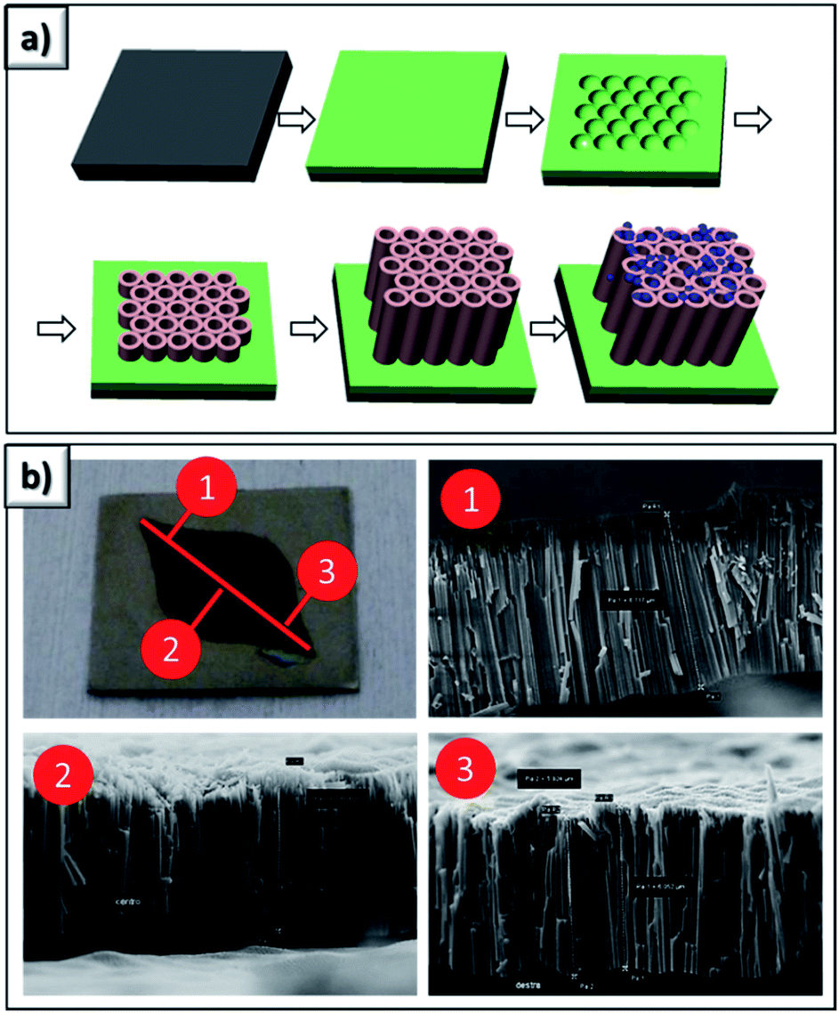 | ||
| Fig. 2 3D scheme representing the TiO2 NTs growth by anodic oxidation (a) and FESEM micrographs (b) showing the cross-section of NT arrays in three different places along the diagonal of the sample (from inlet to outlet). | ||
Thanks to the intrinsic reversible sealing of the microfluidic cell, Field Emission Scanning Electron Microcopy (FESEM) investigation is allowed in order to have information at the different process steps.
The final appearance of the TiO2 NTs array after the microfluidic growth is shown in Fig. 2b. FESEM cross section images collected in different places along the diagonal of the growth area confirm the uniformity of the microfluidic anodization: a constant thickness of about 6 μm was obtained for 10 minutes treatment in the electrolytic solution. As comparison, TiO2 NTs were grown into a standard electrochemical cell and the obtained NTs lengths as a function of the synthesis time are reported in Fig. S1 (see ESI†). Growth rate seems to be weekly dependent by the setup with NTs length slightly higher for the microfluidic configuration. The walls of the tubes are smooth (Fig. S2a†) thanks to the polar organic nature of the electrolytic solution.2 The tubes have an average external diameter of around 110 nm with walls thickness of around 20 nm and exhibit a perfect vertical alignment and hexagonal assembly (see Fig. S2b†).
After the AgNO3 photoreduction the nanotubes surface was fully decorated by Ag nanoparticles. The FESEM images reported in Fig. 3a confirm the uniform distribution of silver NPs along the whole thickness of the NTs array. Higher magnification FESEM images in Fig. 3b allow to appreciate the quasi-hemispherical shape of the Ag NPs with dimension ranging from 10 up to 90 nm (the size distribution evaluated from FESEM images is shown in Fig. S3†).
 | ||
| Fig. 3 FESEM images (a–b) and EDX (c) spectra of TiO2 nanotubes before and after the AgNO3 photoreduction (scale bars in FESEM images are 500 nm in (a) and 100 nm in (b)). | ||
X-ray diffraction (XRD) patterns of as-grown and Ag-decorated TiO2 nanotubes are shown in Fig. S4.† The spectrum of the bare NTs present only peaks associated to titanium substrate since the as-anodized TiO2 nanotubes are fully amorphous. After the Ag synthesis, new peaks appear and can be assigned to the diffraction of (111), (200), and (220) planes of face-centered cubic (fcc) silver (JCPDS card no. 4-783, a = 4.08 Å).
Chemical composition of the nanostructured thin film was investigated using EDX analysis. The EDX spectra (Fig. 3c) exhibit C, F, O, Ag, and Ti peaks, showing that the prepared materials are composed of Ag and TiO2 with the presence of fluorine and carbon atoms, as confirmed by the semi-quantitative standard-less analysis (Table S1†). This contamination is consistent with the study of Albu et al.29 that described the TiO2 NTs as composed by two layers: an outer part (shell) of pure and dense TiO2 and an inner porous part (core) containing electrolyte components.
The UV irradiation induces two secondary effects in addition to the Ag nanoparticles deposition: the first one is related to the heating of the sample which leads to a partial crystallization of amorphous titania.30 Indeed it is possible to observe the appearance of two peaks in the XRD spectrum associated with the TiO2 in the anatase phase. The second and more important effect consists in the degradation of the contaminants (as reported in Table S1† – showing a reduction of C and F contents after the photoreduction process) arising from the wet electrochemical synthesis. This phenomenon can be attributed both to the above mentioned sample heating (previous studies demonstrate how heat treatments allow to eliminate the presence of contaminants in electrochemically grown TiO2 NTs)2 and to the photocatalytic effect of TiO2.
Optimized Ag decorated TiO2 NTs were employed into a SERS opto-fluidic sensor and they were able to detect cyanine (Cy5) molecules in ethanol solutions injected in the device microchamber at low concentrations (see the top spectrum in Fig. 4 concerning with the Raman analysis of Cy5 diluted in ethanol solution at a concentration of 10−6 M). The SERS measurements were performed by a micro-Raman spectrometer (Renishaw inVia, excitation at 514.5 m) using a long working distance objective to focus/collect the exciting/scattered light (backscattering configuration) on the Ag–TiO2 NT surface through the PDMS top-cover of the device (see Fig. S5†). Fig. 4 shows the typical vibrational bands of the analytes in off-electronic resonance condition, since the excitation photon energy (2.54 eV) is far from the Cy5 absorption band maximum (1.9 eV).
 | ||
| Fig. 4 Raman spectra of Cy5 diluted in ethanol solution at a concentration of 10−6 M injected in the fluidic chamber (some main Raman bands are indicated) hosting the Ag-coated TiO2 NTs. The spectra are collected at different steps of UV-cleaning. | ||
It is worth to underline that the most commonly used Raman substrates (i.e. Au or Ag nanoparticles on dielectric matrices) cannot be easily reused. This could be an important drawback from the economical point of view, but also from the substrates reproducibility standpoint. For these reasons a lot efforts have been addressed in the last years in studying recyclable SERS substrates. The intrinsic photocatalytic activity of metal-oxide nanostructures could be exploited to degrade the analytes molecules after the SERS analysis allowing recyclability for a new detection run.31
The general mechanism of photocatalysis on metal-oxide nanostructures is based on the electron–hole pairs photogeneration under UV light, inducing the reaction with both oxygen and water molecules to promote the oxidation of organic substances. Nevertheless the fast recombination of electric charges in the semiconductor alone could reduce the resulting photocatalytic efficiency. To obtain effective molecules photodegradation the electrons and the holes in semiconductor must be separated to suppress their recombination. The noble metal-decorated metal-oxides are more efficient than their uncoated counterpart since for semiconductor/metal hybrid nanostructures with suitable energy level alignment, electrons can be quickly transferred to metal nanoparticles to achieve charges separation.32,33
Fig. 4 shows the Raman spectra of Ag-coated TiO2 NTs impregnated with Cy5 in ethanol solution after UV-exposure at increasing irradiation times. In particular, after an exposure for 30 min the vibrational spectrum of Cy5 is completely quenched. Actually, the photocatalytic process responsible of the shown spectra evolution can be explained by an electrochemical mechanism: the Ag decorated TiO2 NTs array serves as an electron relay for an oxidant and reductant, and electron transfer occurs on the surface of the silver nanoparticles supported on the TiO2 NTs. Cy5 molecules can be photodegradated thanks to electrons transfer from the Ag to the TiO2 conduction band, and conversely, holes transfer from the TiO2 valence band to the Ag under UV excitation. Exploiting the superior photocatalytic properties of combined Ag–TiO2 nanostructures, the SERS substrate can be finally self-cleaned under UV irradiation in order to allow its recycled use. FESEM characterization on UV-cleaned samples have been performed in order to assess the structural stability of the Ag decorated TiO2 NTs. As it is possible to see in Fig. S6,† UV-cleaning does not show any influence on the samples morphology. This observation is in line with previously reported analysis on UV-cleaned recyclable SERS substrates.18
Conclusions
In summary, metal-semiconductor nanostructures consisting of Ag-coated TiO2 NTs have been fully synthesized in a microfluidic electrochemical reactor exploiting in situ anodic oxidation and in situ silver nitrate photoreduction. Vibrational spectroscopy analysis confirms their promising application as recyclable SERS-active substrates for opto-fluidic molecular sensors. Moreover the suitable energy level alignment in the obtained semiconductor/metal hybrid nanostructures could be exploited to degrade analyte molecules after the SERS analysis allowing substrate recyclability.Additionally the here reported study can be exploited and extended to the microfluidic anodic oxidation of several other metals (valve metals such as Al, Ta, Va, Zr, Nb, Hf, Mg, …) leading to nanostructured functional oxides largely investigated for different applications from sensing to energy harvesting and storage.
Acknowledgements
Authors would like to thank Dr Stefano Bianco for XRD measurement and Dr Angelica Chiodoni for the help during FESEM characterization. The research has received funding from the Italian Flagship Project NANOMAX (Progetto Bandiera MIUR PNR 2011–2013) and the Italian FIRB 2011 NEWTON (RBAP11BYNP).Notes and references
- H. P. Jen, M. H. Lin, L. L. Li, H. P. Wu, W. K. Huang, P. J. Cheng and E. W. G. Diau, ACS Appl. Mater. Interfaces, 2013, 5, 10098 CAS.
- A. Lamberti, A. Sacco, S. Bianco, D. Manfredi, M. Armandi, M. Quaglio, E. Tresso and C. F. Pirri, Sol. Energy, 2013, 95, 90 CrossRef CAS.
- Z. Bi, M. P. Paranthaman, P. A. Menchhofer, R. R. Dehoff, C. A. Bridges, M. Chi, B. Guo, X.-G. Sun and S. Dai, J. Power Sources, 2013, 222, 461 CrossRef CAS.
- A. Lamberti, N. Garino, A. Sacco, S. Bianco, A. Chiodoni and C. Gerbaldi, Electrochim. Acta, 2015, 151, 222 CrossRef CAS.
- S. Hernández, D. Hidalgo, A. Sacco, A. Chiodoni, A. Lamberti, V. Cauda, E. Tresso and G. Saracco, Phys. Chem. Chem. Phys., 2015, 17, 7775 RSC.
- B. Chen, J. Hou and K. Lu, Langmuir, 2013, 29, 5911 CrossRef CAS PubMed.
- J. Zou, Q. Zhang, K. Huang and N. J. Marzari, J. Phys. Chem. C, 2010, 114, 10725 CAS.
- V. Galstyan, E. Comini, G. Faglia and G. Sberveglieri, Sensors, 2013, 13, 14813 CrossRef.
- M. Y. Lan, C. P. Liu, H. H. Huang, J. K. Chang and S. W. Lee, Nanoscale Res. Lett., 2013, 8, 1 CrossRef.
- S. Liu and A. Chen, Langmuir, 2015, 21, 8409 CrossRef.
- K. Lee, D. Kim, S. Berger, R. Kirchgeorg and P. Schmuki, J. Mater. Chem., 2012, 22, 9821 RSC.
- Y. Tang, J. Tao, Z. Dong, J. T. Oh and Z. Chen, Adv. Nat. Sci.: Nanosci. Nanotechnol., 2011, 2, 045002 CrossRef.
- S. So, K. Lee and P. Schmuki, J. Am. Chem. Soc., 2012, 134, 11316 CrossRef CAS PubMed.
- R. Li, A. Zhou, Q. Lu, C. Yang and J. Zhang, Colloids Surf., A, 2013, 436, 270 CrossRef CAS.
- S. Nitta, A. Yamamoto, M. Kurita, R. Arakawa and H. Kawasaki, ACS Appl. Mater. Interfaces, 2014, 6, 8387 CAS.
- Y. Huang, L. Sun, K. Xie, Y. Lai, B. Liu, B. Ren and C. J. Lin, Raman Spectrosc., 2011, 42, 986 CrossRef CAS.
- Y. Chen, G. Tian, K. Pan, C. Tian, J. Zhou, W. Zhou, Z. Ren and H. Fu, Dalton Trans., 2012, 41, 1020 RSC.
- X. Li, G. Chen, L. Yang, Z. Jin and J. Liu, Adv. Funct. Mater., 2010, 20, 2815 CrossRef CAS.
- A. Lamberti, A. Virga, A. Chiadò, A. Chiodoni, K. Bejtka, P. Rivolo and F. Giorgis, J. Mater. Chem. C, 2015, 3, 6868 RSC.
- L. Yang, P. Li, H. Liu, X. Tang and J. Liu, Chem. Soc. Rev., 2015, 44, 2837 RSC.
- E. J. Blackie, E. C. L. Ru and P. G. Etchegoin, J. Am. Chem. Soc., 2009, 131, 14466 CrossRef CAS PubMed.
- Q. Li, B. Li and Y. Wang, RSC Adv., 2013, 3, 13015 RSC.
- J. Qi, J. Zeng, F. Zhao, S. H. Lin, B. Raja, U. Strych, R. C. Willson and W. C. Shih, Nanoscale, 2014, 6, 8521 RSC.
- A. Lamberti, A. Virga, A. Angelini, A. Ricci, E. Descrovi, M. Cocuzza and F. Giorgis, RSC Adv., 2015, 5, 4404 RSC.
- M. Ladanov, P. Algarin-Amaris, G. Matthews, M. Ram, S. Thomas, A. Kumar and J. Wang, Nanotechnology, 2013, 24, 375301 CrossRef CAS PubMed.
- S. K. Yoon, G. W. Fichtl and P. J. Kenis, Lab Chip, 2006, 6, 1516 RSC.
- O. Scialdone, C. Guarisco and A. Galia, Electrochim. Acta, 2011, 58, 463 CrossRef CAS.
- A. Lamberti, M. Quaglio, A. Sacco, M. Cocuzza and C. F. Pirri, Appl. Surf. Sci., 2012, 258, 9427 CrossRef CAS.
- S. P. Albu, A. Ghicov, S. Aldabergenova, P. Drechsel, D. LeClere, G. E. Thompson, J. M. Macak and P. Schmuki, Adv. Mater., 2008, 20, 4135 CAS.
- O. Van Overschelde, R. Snyders and M. Wautelet, Appl. Surf. Sci., 2007, 254, 971 CrossRef CAS.
- X. Li, H. Hu, D. Li, Z. Shen, Q. Xiong, S. Li and H. J. Fan, ACS Appl. Mater. Interfaces, 2012, 4, 2180 CAS.
- A. Lamberti, Metal-Oxide Nanostructures for Surface Enhanced Raman Spectroscopy, in Encyclopedia of Nanotecnology, ed. B. Bhushan, Springer, Dordrecht, 2015, in press Search PubMed.
- L. Yang, P. Li and J. Liu, RSC Adv., 2014, 4, 49635 RSC.
Footnote |
| † Electronic supplementary information (ESI) available: XRD measurements, additional FESEM characterizations and experimental details. See DOI: 10.1039/c5ra23434d |
| This journal is © The Royal Society of Chemistry 2015 |