DOI:
10.1039/C5RA23427A
(Paper)
RSC Adv., 2016,
6, 910-917
Triboelectric generator composed of bulk poly(vinylidene fluoride) and polyethylene polymers for mechanical energy conversion†
Received
6th November 2015
, Accepted 14th December 2015
First published on 16th December 2015
Abstract
We designed a stable triboelectric generator (TEG) consisting of a new combination of poly(vinylidene fluoride) (PVDF) and polyethylene (PE) films which shows prospect for easy and low cost device fabrication. Both PE and PVDF are selected from the negative side of the triboelectric series considering the difference in charge affinity. An open circuit peak-to-peak output voltage of ∼20 V and current density ∼0.34 A m−2 were obtained just by striking the TEG manually. The effect of directional forces on the TEG was studied for future anisotropic pressure sensor fabrications. The charging capacity of the TEG was checked by using a commercially available capacitor revealing the prospect of battery charging. Furthermore, the TEG powered at least 12 commercial white light emitting diodes which indicates its potential use as a carbon emission free power source suitable for portable electronic devices.
Introduction
Unconventional energy harvesting technologies are of great interest in renewable and green energy application areas. In this regard, different types of energy generation mechanisms have been adopted including photoelectric effect,1–5 vibration energy harvesting,6,7 thermoelectric conversion,8–10 piezoelectric phenomena11–15 and the triboelectric effect.16–18 Of these, piezoelectric and triboelectric energy generation from polymer based materials has received increasing interest recently because of their flexible, durable, and light weight properties. Being mechanical energy harvesting systems, these generators are effective and promising to use as self-powered electronic devices, touch sensors and electronic skins.19–22 Piezoelectric generators are based on materials that have the ability to transform applied mechanical strain into electric potential via a change in dipole moments.11 On the other hand, triboelectric generator (TEG) response is based on the transfer of electrons from one material to another when two materials with different charge affinity come into contact and then separate.16 This simple working principle makes the TEG relatively cost-effective and largely scalable in comparison to the piezoelectric generators for mechanical energy harvesting since the materials for TEG are largely abundant. Hence, the central focus is to generate energy using tribo-electrification to boost up the output power for effective power source for practical applications. In addition, the output power from piezoelectric generator often combines the contribution of both piezoelectric and triboelectric effects. For example if triboelectric effect occurs within a piezoelectric generator due to friction between the active piezoelectric materials. Similarly in a TEG, piezoelectricity can affect the resulting charge generation if a piezoelectric material is used in the device fabrication. Hence, fundamentally it is important to separate the effect of triboelectricity and piezoelectricity within a mechanical power generator device.
In this work, we report on the fabrication of triboelectric generator using the combinations of two cost-effective polymers, namely, poly(vinylidene fluoride) (PVDF) and polyethylene (PE). For fabricating triboelectric generator, active materials are usually chosen from positive and negative sides of triboelectric series.16,22–24 However, both PE and PVDF are selected from negative side of triboelectric series considering their difference in charge affinity and to testify the device efficiency when materials combinations in TEG are chosen from the negative side of triboelectric series. Since PVDF is a well-known piezoelectric material,19,25 we have fabricated the device structure in such a way that only one surface of the PVDF film remains connected to the electrode. Hence, the effect of piezoelectricity within the triboelectric generator can be avoided since piezoelectricity occurs only when both the surface of the film is connected to electrodes. We have also tested the effects of directional forces in TEG that attributes to potential use as anisotropic pressure sensors applications along with the harvesting mechanical energy. We have obtained peak-to-peak output voltages of ∼20 V with an output short circuit current of ∼31 μA from the TEG under vertically applied forces that promises to the wide range applications to directly power up several tiny portable electronic gadgets. Furthermore, our TEG can differentiate the weight differences of coins, which enables it to be used as a self-powered pressure sensor.
Experimental details
Fabrication
TEG was fabricated in sandwich pattern using two rectangular steel plates (0.8 mm thick) as top and bottom electrodes. PE tape was first attached to one steel electrode. PVDF solution was prepared by mixing 1 g of PVDF pallets (Sigma-Aldrich, USA) with 4 mL dimethylformamide (DMF). The solution was stirred at 60 °C for 4 h. Then 4 mL acetone was mixed to it and stirred at room temperature. PVDF film was fabricated on top of another steel electrode by drop cast method from resulting PVDF solution. Afterwards, the PVDF–steel electrode was annealed for an hour at 60 °C under nitrogen environment. The thickness of PE and PVDF film was ∼0.14 mm and ∼15 μm respectively. We ensured that the PVDF film was continuous and fully attached to the electrode. In the next step, PE–steel electrode and the PVDF–steel electrodes were stacked together in form of a sandwich pattern device with an effective area of 9 cm2 (Fig. 1a). A thick elastic tape lock at one edge of the device is attached so that PVDF and PE remain separated (Xmax, maximum separation is 4 mm) in absence of any external force (Fig. 1b). For electrospun PVDF based TEG, the electrospinning of the PVDF is employed by horizontal electrospinning method. The solution of PVDF was loaded into a syringe fitted with a metallic needle and kept at 15 cm away from the steel electrode collector. Electrospinning was performed by employing a high voltage of 15 kV with the feed rate of 1 mL h−1.
 |
| | Fig. 1 (a) Schematic structure of the TEG layer by layer. (b) Schematic of the TEG after attaching the tape to separate the polymer materials when no mechanical force is applied. (c) Forward connection and (d) reverse connection of the TEG to the oscilloscope. | |
Measurements
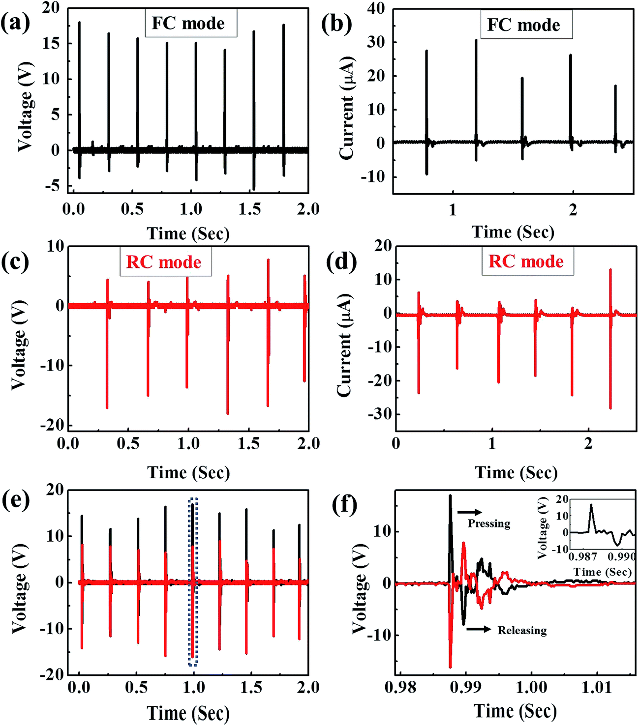
Output voltage from the device under periodic external forces was measured by a digital oscilloscope (Yokogawa DL1620). Output current of the device was measure by Keysight B2987A picoammeter. Periodic force was applied manually with a wooden piece. When the positive probe of the oscilloscope was connected to the PVDF–steel electrode and the ground was connected to the PE–steel electrode, it was treated as the forward connection (FC), (Fig. 1c). The inverted connection was defined as the reverse connection (RC), as shown in Fig. 1d.
Results and discussion
The mechanism of the output voltage generation is schematically shown in Fig. 2. When the electrodes are separated from each other, the device remains in equilibrium state (Fig. 2a). Upon applying the first striking force to the device, PVDF and PE films touch and rub against each other. This generates electrostatic charges with opposite signs, which are distributed on the surface of two polymer films. In this case, PVDF becomes negatively charged and PE becomes positively charged according to the triboelectric series (Fig. 2b).26 However, at this point, these charges will not induce any charges on the electrodes since the positive and negative charges are situated close to each other. Just after the striking, the device relaxes owing to the flexibility induced by the attached thick elastic tape. During the process, the polymer films are separated from each other inducing static charges on the counter electrodes. Negatively charged PVDF film will induce positive charges on the electrode attached to it at the near end. Similarly, positively charged PE film will induce negative charges on the electrode attached to it at the near end. In this configuration, the counter charges located at the far ends of the electrodes will move to the opposite electrodes making these more positive and negative in nature (Fig. 2c). This process induces the flow of free electrons through the external load generating negative peak for FC. The current will continue till induced charges flow to the electrodes (Fig. 2d). However, the charges on both the polymer surfaces remain static owing to the insulating nature of PVDF and PE. After applying the next striking force, the electrodes approach into closer proximity (Fig. 2e) and finally touch each other mimicking previous structure as on Fig. 2b. While the separation between the two polymers is decreasing, positively charged PE will repel the induced positive charges on the electrode attached to PVDF. This will create flow of free electrons towards the PVDF-electrode generating a positive peak for FC. Current will continue till the two polymers come in contact with each other and charges are neutralized from the electrodes (Fig. 2b). These cycles continue repetitively with the applied periodic forces.
 |
| | Fig. 2 Mechanism of the TEG when pressed and released. (a) The device at rest before applying any forces. No charges are built up on the surfaces of the polymers. (b) Charge distribution in the device after first striking. At this point, no charges have been induced on the electrodes as the negative charges on PVDF surface and the positive charges on PE surface are close to each other. (c) Induction of the charges on the electrodes and flow of charges through external load while the device is being released and the distance between the two polymer surfaces is increasing. (d) Electrostatic equilibrium state when the electrodes are fully induced. (e) Charge distribution and charge flowing direction when the distance between the electrodes is decreasing while the external force is withdrawn. | |
In order to investigate the output performance of the TEG, periodic forces were applied manually on the device from different directions. The output signals from TEG for the vertically applied forces are shown in Fig. 3. An open circuit peak-to-peak output voltage of ∼20 V (Fig. 3a) and short circuit current of ∼31 μA (Fig. 3b) was obtained in FC mode. The absolute value of the short circuit transferred charges (Qsc) in a half cycle was found to be 0.0267 μC (calculated by integrating a single current peak in half cycle). We reversed the connection (RC mode) to verify the actual output from the TEG and its consistency. Similar output characteristics (Fig. 3c and d) were obtained from the TEG in RC mode as well. For further clarification of the output characteristics, the output characteristics from the two electrodes were simultaneously connected to two channels of a digital oscilloscope, the corresponding results are shown in Fig. 3e. The enlarged image of one peak of Fig. 3e is presented in Fig. 3f, which shows the signals from two electrodes are exactly opposite to each other. Additionally, we have measured the Fourier transform infrared spectroscopy (FTIR) of the drop casted PVDF (Fig. 4a and b). The strong peaks at 766 cm−1 and 795 cm−1 indicate the presence of α-phase in the film, whereas the presence of β and γ-phases are assigned from the peaks at 1279 cm−1 and 1233 cm−1.25 To quantify the relative proportion of electroactive β and γ-phases, we have deconvoluted the FTIR spectra (915–760 cm−1 regions). Absorption intensity at 840 cm−1 conveys dual characteristics of both β and γ-electroactive phases (FEA). The relative proportion of electroactive phases (FEA) attributed to both β and γ-phases can be calculated using the following equation:
| |
 | (1) |
where,
I766 and
IEA are the absorbance intensity at 766 cm
−1 and 840 cm
−1, respectively;
K766 and
K840 are the absorption coefficient at the respective wavenumbers.
27 From the deconvoluted curve (
Fig. 4b), calculated electroactive phase (
FEA) is found to be 60%. The individual β and γ-phases are calculated by curve deconvolution of the 840 cm
−1 band, where the broadening contribution due to γ-phase and the sharp, well resolved peak for β-phase have been considered.
 |
| | Fig. 3 Output voltages and currents of the TEG under a periodic force applied through a wooden piece by hand. (a) Output voltage of the TEG for forward connection (FC), (b) short circuit current of the TEG for FC, (c) output voltage of the TEG for reverse connection (RC), (d) short circuit current of the TEG for RC, (e) output voltage from the two electrodes simultaneously, (f) zoomed image of one peak of (e), position of the peak for pressing and releasing is shown for the black curve, i.e., for the FC. Inset shows zoomed picture of first peak of black curve in (f). | |
 |
| | Fig. 4 (a) FTIR spectrum of drop casted PVDF film. (b) Deconvoluted FTIR spectra (915–760 cm−1) of drop casted PVDF film. Corresponding PVDF phases are marked in the figure. | |
The following equations are used to quantify the relative proportion of electroactive β and γ-phases individually.25
| |
 | (2a) |
| |
 | (2b) |
where,
Aβ and
Aγ are the integrated areas under the β and γ-marked deconvoluted curves in
Fig. 3d centered at the 840 cm
−1 band. The individual
F(β) and
F(γ) are found to be ∼20% and ∼40% respectively. This indicates that the contribution from γ-phase to the relative proportion of electroactive phases (
FEA) is higher than the contribution from β-phase. The lower proportion of β-phase suggests that the output response is not coming from piezoelectricity of PVDF film. Additionally, the introduction of PE film within the TEG rule out any output voltage that may have originates from piezoelectricity. These observations support the fact that the output signals of the TEG arise due to triboelectric effect only.
The role of rough surfaces to generate more surface charges during friction for enhanced triboelectric effect was demonstrated earlier.24 Surface morphologies of the drop casted PVDF film and PE tape were studied using Scanning Electron Microscope (SEM) (Fig. 5a and b). Randomly distributed fibril structures in each spherulites forming a rough surface are observed in the drop casted PVDF film. Such surface roughness is beneficial for the TEG device performance. In comparison to the PVDF film, the surface morphology of polyethylene film appears relatively smooth (Fig. 5b, for example, red marked regions). Hence, few scratches were made manually on the surface of the PE film to induce surface roughness which is supposed to increase the friction between PVDF and PE film within the TEG. For further investigation on the effect of film roughness on the TEG device performance, we have prepared TEG consisting of electrospun PVDF fibers instead of drop casted PVDF film. Surface morphology of the electrospun PVDF film was studied in SEM (Fig. 5c). The output voltages of the TEGs consisting of smooth PE, scratched PE and electrospun PVDF (with scratched PE) film are compared in Fig. 5d. Maximum peak-to-peak output voltage for TEG consisting of smooth PE and drop casted PVDF is found to be ∼12 V which is much lower than that of TEG consisting of scratched PE and drop casted PVDF. Maximum peak-to-peak output voltage for the electrospun PVDF and scratched PE based TEG is found to be ∼14 V which is relatively lower than the output voltage of the drop cast PVDF based TEG. Lower output voltage for the electrospun PVDF based TEG in comparison to the drop cast PVDF based TEG may be attributed to the lower effective contact area of electrospun PVDF fibers with PE film and its poor adhesion with steel electrodes, especially as per adopted device geometry is concerned.
 |
| | Fig. 5 FE-SEM images of (a) drop casted PVDF film and (b) polyethylene tape. Scratches are shown by white arrows and red loops show the smooth surfaces. (c) SEM image of the electrospun PVDF and (d) comparison of output voltages from different TEGs consisting of smooth PE, scratched PE and electrospun PVDF respectively. | |
To study the effect of directionality of hammering forces, we used the TEG without the thick elastic tape which was used previously for electrode separation. We have applied the forces in ∼40° and ∼60° angles on the upper steel electrode so that the electrode along with the PVDF film slides a little on the PE film and causes separation of charges. The results were compared with that of the TEG with vertical forces (90°). Schematic for applied forces from different directions and their effect on output voltages are given in Fig. 6. Fig. 6d shows the output voltage for the applied sliding forces on the upper electrode with ∼40° angle as shown in Fig. 6a. Fig. 6e shows the output voltage for the same system under the sliding force with a higher angle ∼60°. Corresponding schematic diagram is shown in Fig. 6b. Fig. 6f shows the output voltage of the TEG under vertical forces, which is perpendicular to the top electrode (Fig. 6c). When the direction of applied force is the lowest (Fig. 6a), the output voltage is found to be the lowest in comparison to other two directions. This observation clearly shows that the output voltage increases with increasing the striking angle with respect to the top electrode. This is due to the fact that when the sliding of the top electrode occurs, negative charges are accumulated on PVDF surface and positive charges will be generated on PE surface. Since sliding of the surfaces takes relatively longer time, the charges generated on two polymer surfaces will not be separated immediately. As a result, the possibility of recombination of negative charges on PVDF with the positive charges on PE will increase resulting in lower output voltage. When the striking angle is increased (Fig. 6b), the sliding occurs for lesser time diminishing the possibility of charge recombination, thus increasing the output voltage. For vertical forces, the polymers come to contact for a little period of time and polymers are separated immediately after the strike. As a result, the charges on the surfaces of two polymers have lesser possibility of recombination resulting in higher output voltage. The process is reinforced by the use of thick elastic tape (Fig. 1b) in the TEG, which helps the polymers to be separated immediately after applying the vertical force enabling efficient in energy generation.
 |
| | Fig. 6 Schematic diagram for different types of forces on the TEG with no thick elastic tape attached. Sliding force is applied on the upper electrode (a) at ∼40° angle and (b) at 60° angle. (c) Vertical force (90° angle) is applied on the upper electrode. Output voltage for the TEG, when no thick elastic tape is used, with sliding forces at ∼40° (d) and at ∼60° (e). (f) Output voltage for the TEG under vertical forces. | |
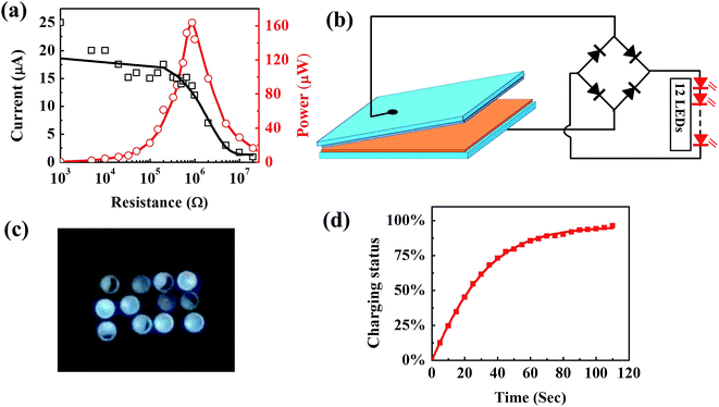
For application of the TEG as a power source, the effective electric power generation is estimated by connecting different resistors as external load.19 Output currents and power outputs (W = Ipeak2R) are plotted for different load resistances (Fig. 7a). The current decreases with increasing load resistance due to ohmic loss.24 Maximum instantaneous output power reaches to 160 μW for 900 kΩ of load resistance with power density 0.178 W m−2 signifying that our TEG is quite efficient for the particular load resistance. To show the practical implementation of our TEG, we have connected few commercial white light emitting diodes (LEDs) with the TEG using a typical bridge rectifier circuit (Fig. 7b). It was able to power up at least 12 white LEDs intensely by simply tapping with hand, the concerning snapshot provided in Fig. 7c (ESI, Video S1†). This clearly illuminated the bread broad where even individual connecting holes were also clearly visible, indicating to use as an effective energy harvesting power source for decorating with LEDs and illuminating the roads where the mechanical stimuli can be directly utilized from the environment. The charging capacity of TEG was checked by connecting a commercial capacitor (2.2 μF) through a bridge rectifier and striking the TEG at 3 Hz of frequency and subsequently measured the voltage across the capacitor. The transient response of capacitor charging is shown in Fig. 7d. This implies that the energy of the TEG can be stored by charging a battery for further use.
 |
| | Fig. 7 (a) Current versus resistance (black curve) and output power versus resistance (red curve). (b) Schematic of the TEG and circuit diagram for powering the LEDs. (c) Snapshot of powering LEDs from TEG by applying periodic vertical forces. (d) Transient response of the capacitor, when connected with the TEG through a bridge rectifier. | |
Our TEG showed potential to be used as a self-powered pressure sensor as it generates voltage or current through contact electrification between two triboelectric materials by external mechanical force. To illustrate this capability, some standard Indian coins carrying different weights were dropped from a fixed height to the central area of the TEG. The TEG was covered with a paper piece to avoid any charge flow upon contact between coins and electrode. When a coin drops on the TEG, PVDF and PE come into contact with each other, leading to a detectable signal output. Fig. 8 illustrates the coin drop test for application of the TEG as a self-powered pressure sensor. Different types of coins (1 rupee, 2 rupee, 5 rupee and 10 rupee) were used and dropped from a height of ∼15 cm on the central area of the TEG. The peak voltage response for various types of coin with different masses is plotted in Fig. 8b. Expectedly, the heaviest coin generates the maximum output voltage.
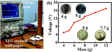 |
| | Fig. 8 Illustration of the TEG used as a self-powered pressure sensor. (a) Setup image of the coin drop test. Coins of different mass are dropped from a height of about 15 cm on the TEG. Instant response can be seen from the voltage peak in the image. (b) The peak voltage response for various types of coins. Inset shows the picture of different types of coins used. | |
Conclusions
In summary, we developed a very simple method to fabricate a stable triboelectric generator consisting of PVDF and PE films. We are able to rule out the piezoelectricity effect, which may originate from PVDF film/electrospun fibers within the TEG by introducing PE films within the device geometry. The TEG shows prospect of easy and low cost device fabrication with high electrical output performance. Furthermore, the effect of directional forces on TEG is studied for verifying the harvesting mechanical energy capability and also futuristic pressure anisotropic sensor fabrications. The TEG gives open circuit peak-to-peak output voltage of ∼20 V and maximum short circuit current of ∼31 μA with current density ∼0.34 A m−2 just by striking the TEG manually with a wooden piece. Moreover, the TEG is able to power at least 12 commercially white LEDs directly just by tapping with hand indicating a potential use as carbon emission free power source suitable in portable electronic devices, lighting the roads, transportation monitoring and so on. Furthermore, the TEG is used to differentiate the mass of different coins. This study opens up the possibility of the TEG to utilize in self-powered power sensor. The easy fabrication of TEG consisting of a new combination of polymers may add an additional benefit for batch fabrication and easy commercialization.
Acknowledgements
Financial support from SERB (EMR/2014/000664), DST, India is gratefully acknowledged. P. K. S. and G. S. K. gratefully acknowledge the DST-INSPIRE fellowship. S. M. and K. C. S. gratefully acknowledge CSIR, India for fellowship.
References
- M. Grazel, Nature, 2001, 414, 338–344 CrossRef PubMed.
- A. H. Khan, U. Thupakula, A. Dalui, S. Maji, A. Debangshi and S. Acharya, J. Phys. Chem. C, 2013, 117, 7934–7939 CAS.
- K. A. Mazzio and C. K. Luscombe, Chem. Soc. Rev., 2015, 44, 5744 RSC.
- W. Chaikittisilp, K. Ariga and Y. Yamauchi, J. Mater. Chem. A, 2013, 1, 14–19 CAS.
- B. Tian, X. Zheng, T. J. Kempa, Y. Fang, N. Yu, G. Yu, J. Huang and C. M. Lieber, Nature, 2007, 449, 885–889 CrossRef CAS PubMed.
- S. P. Beeby, R. N. Torah, M. J. Tudor, P. Glynne-Jones, T. O'Donnell, C. R. Saha and S. Roy, J. Micromech. Microeng., 2007, 17, 1257–1265 CrossRef.
- R. Torah, P. Glynne-Jones, M. Tudor, T. O'Donnell, S. Roy and S. Beeby, Meas. Sci. Technol., 2008, 19, 125202 CrossRef.
- D. Kraemer, B. Poudel, H. P. Feng, J. C. Caylor, B. Yu, X. Yan, Y. Ma, X. Wang, D. Wang, A. Muto, K. McEnaney, M. Chiesa, Z. Ren and G. Chen, Nat. Mater., 2011, 10, 532–538 CrossRef CAS PubMed.
- L. E. Bell, Science, 2008, 321, 1457–1461 CrossRef CAS PubMed.
- R. Venkatasubramanian, E. Siivola, T. Colpitts and B. O'Quinn, Nature, 2001, 413, 597–602 CrossRef CAS PubMed.
- Z. L. Wang and J. H. Song, Science, 2006, 312, 242–246 CrossRef CAS PubMed.
- R. A. Whiter, V. Narayan and S. Kar-Narayan, Adv. Energy Mater., 2014, 4, 1400519 Search PubMed.
- R. Yang, Y. Qin, L. Dai and Z. L. Wang, Nat. Nanotechnol., 2009, 4, 34–39 CrossRef CAS PubMed.
- X. Wang, J. Song, J. Liu and Z. L. Wang, Science, 2007, 316, 102–105 CrossRef CAS PubMed.
- K. Park, J. H. Son, G. T. Hwang, C. K. Jeong, J. Ryu, M. Koo, I. Choi, S. H. Lee, M. Byun, Z. L. Wang and K. J. Lee, Adv. Mater., 2014, 26, 2514–2520 CrossRef CAS PubMed.
- S. Wang, L. Lin and Z. L. Wang, Nano Lett., 2012, 12, 6339–6346 CrossRef CAS PubMed.
- S. Wang, S. Niu, J. Yang, L. Lin and Z. L. Wang, ACS Nano, 2014, 8, 12004–12013 CrossRef CAS PubMed.
- G. Cheng, Z. H. Lin, Z. Du and Z. L. Wang, Adv. Funct. Mater., 2014, 24, 2892–2898 CrossRef CAS.
- A. Tamang, S. K. Ghosh, S. Garain, M. M. Alam, J. Haeberle, K. Henkel, D. Schmeisser and D. Mandal, ACS Appl. Mater. Interfaces, 2015, 7, 16143–16147 CAS.
- W. Seung, M. K. Gupta, K. Y. Lee, K. S. Shin, J. H. Lee, T. Y. Kim, S. Kim, J. Lin, J. H. Kim and S. W. Kim, ACS Nano, 2015, 9, 3501–3509 CrossRef CAS PubMed.
- X. Li, Y. H. Wang, C. Zhao and X. Liu, ACS Appl. Mater. Interfaces, 2014, 6, 22004–22012 CAS.
- Y. Yang, H. Zhang, X. Zhong, F. Yi, R. Yu, Y. Zhang and Z. L. Wang, ACS Appl. Mater. Interfaces, 2014, 6, 3680–3688 CAS.
- J. A. Cross, Electrostatics: Principles, Problems and Applications, Adam Hilger, Bristol, 1987 Search PubMed.
- Y. Zheng, L. Cheng, M. Yuan, Z. Wang, L. Zhang, Y. Qin and T. Jing, Nanoscale, 2014, 8, 7842–7846 RSC.
- S. Maji, P. K. Sarkar, L. Aggarwal, S. K. Ghosh, D. Mandal, G. Sheet and S. Acharya, Phys. Chem. Chem. Phys., 2015, 17, 8159–8165 RSC.
- Y. Zi, S. Niu, J. Wang, Z. Wen, W. Tang and Z. L. Wang, Nat. Commun., 2015, 6, 8376 CrossRef CAS PubMed.
- R. Gregorio Jr and M. Cestari, J. Polym. Sci., Part B: Polym. Phys., 1994, 32, 859–870 CrossRef.
Footnote |
| † Electronic supplementary information (ESI) available. See DOI: 10.1039/c5ra23427a |
|
| This journal is © The Royal Society of Chemistry 2016 |
Click here to see how this site uses Cookies. View our privacy policy here.