Bhaskar Dudem,
Jung Woo Leem and
Jae Su Yu*
Department of Electronics and Radio Engineering, Institute for Wearable Convergence Electronics, Kyung Hee University, 1732 Deogyeong-daero, Giheung-gu, Yongin-si 446-701, South Korea. E-mail: jsyu@khu.ac.kr
First published on 21st December 2015
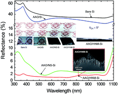
We fabricated hierarchical nano/micro (HNM) architectures on a silicon (Si) surface for efficient antireflection. To form the micropyramid (MP) structures on the Si surface, a potassium hydroxide-based wet etching process was carried out. Meanwhile, for the nanostructures (NS), an anodic aluminum oxide (AAO) film with nanopores as an etch mask was used, followed by an inductive coupled plasma (ICP) etching process. To obtain optimized structures with efficient antireflection, the etching was performed under different process conditions including RF power, ICP power, process pressure, gas flow rate, and etching time. The AAO/NS-Si largely reduced the reflectivity of bare Si over a wide wavelength range of 300–1100 nm, showing an average reflectance (Ravg) value of 3.4% (i.e., Ravg = 38% for the bare Si). The AAO/HNM-Si consisting of NS/MP arrays had a lower reflectance spectrum than 2% at wavelengths of 300–1050 nm, exhibiting an Ravg value of 1.5%. Superior antireflection characteristics were also observed in the wide light incident angle range of 20–70° at wavelengths of 300–1100 nm. For theoretical analysis, reflectance calculations were also performed by a rigorous coupled-wave analysis simulation, which indicated a similar trend to the experimental results. For surface wetting behavior, it revealed a superhydrophilic surface with water contact angles of < 5°.
Fig. 1 Schematic diagram for the fabrication of (a) the NS and (b) the HNM structures on Si substrates via an AAO etch mask with nanopores. The SEM images of AAO film on the Si substrate are shown. |
For theoretical optical analyses of the samples, the RCWA calculations were performed using a commercial software package (Diffract MOD, Rsoft Design Group). To simply design the theoretical model, as shown in Fig. S1 of the ESI,† the random geometry of the AAO nanopores with a cylindrical shape on the Si substrate is roughly represented in the Cartesian coordinate system by a scalar-valued function of three variables, f(x, y, z). The nanopore diameter and average period between the nanopores were set to be 80 nm and 100 nm, respectively. For the NS on the surface of Si, the inversely tapered cylindrical model with the bottom diameter of 10 nm was used. The thicknesses of AAO film and Si substrate were also kept to be 150 nm and 500 μm. Further details can be found in our previous work.32,41 The refractive index and extinction coefficient of the constituent materials (i.e., AAO and Si) used in these calculations were acquired from the index web site.42
To investigate the influence of etching parameters on the reflectance of AAO/NS-Si, the etching process was carried out at different conditions of RF power, ICP power, process pressure, etching time, and additional Ar gas flow rate. Fig. 3 shows the (a) side-view SEM images and (b) measured reflectance spectra of the AAO/NS-Si at different RF powers. For comparison, the reflectance spectra of bare Si and AAO/Si are also shown in Fig. 3(b). The etching process was performed at the fixed ICP power of 200 W, process pressure of 10 mTorr, and etching time of 400 s. From the SEM images in Fig. 3(a), the etched profile (i.e., thickness of AAO films and height of Si NS) clearly depends on the RF power. With increasing the RF power from 25 to 125 W, the thickness of AAO films and height of Si NS were decreased from 280 to 150 nm and increased from 200 to 370 nm, respectively. Therefore, the variations in AAO film thickness and Si NS height were attributed to the enhancement of etch rate at higher RF powers. The tapered sharp shape of Si NS can be observed at high RF powers. This is ascribed to the cylindrical structure of AAO with a round bottom barrier layer,44 as shown in the cross-sectional SEM image of Fig. 1. Although the pore widening was carried out, the barrier layer close to the pore wall still remained slightly. During the etching, therefore, the faster etching at the center of barrier layer/Si and the slower etching at the side of barrier layer/Si were performed, respectively, thus producing the tapered Si NS with a sharp peak. Also, the chemical reaction might be relatively dominant (i.e., isotropic etching surface profile) during the etching.45,46 In fact, the etching reactions are also strongly dependent on the etching parameters such as pressure, gas flow rate, RF power, ICP power, etc. From Fig. 3(b), the bare Si has a high reflectance spectrum of > 30% in the wavelength region of 300–1100 nm (i.e., Ravg = 39% at λ = 300–1100 nm). However, the introduction of AAO films into the Si surface causes the lower reflectance compared to the bare Si due to its intermediate refractive index (i.e., nAAO < 1.76) between air (n = 1) and the Si (nSi ∼ 3.6), as mentioned in Fig. 2.32 For the NS-Si, the AAO film further suppresses the surface reflectivity, as shown in Fig. S2 of ESI.† But the reflectance of the AAO/Si with a planar structure is still high (i.e., Ravg = 31%). Meanwhile, the AAO/NS-Si samples exhibit much lower reflectance spectra than those of the bare Si and AAO/Si over a wide wavelength range of 300–1100 nm because of their gradient effective refractive index profiles in materials and structures, as mentioned above. Therefore, the reflectance spectrum is decreased from 25 W (i.e., Ravg = 9.4%) to 100 W (i.e., Ravg = 4.5%) due to the AAO film with 150 nm (i.e., close to AAO films with thicknesses around 100 nm) and larger heights of Si NS. Then, it is slightly increased at 125 W (i.e., Ravg = 5.5%). This is ascribed to the reduced AAO film thickness and collapsed Si NS due to the high energetic ion impingement at 125 W of RF power. Also, the high RF power leads to the increased air gap along the interface between the AAO and Si NS.47 Here, there are fluctuations in reflectance spectra of samples due to the constructive or destructive interference at the interfaces since the AAO film with cylindrical nanopores can be regarded as a single medium with an effective refractive index like a thin film, thus forming the multilayer (i.e., AAO/NS-Si) structure with different refractive indices.48 Furthermore, at wavelengths of 300–400 nm, the reflection peak is attributed to the refractive index of crystalline Si.42 At wavelengths around 370 nm, the Si has relatively high refractive indices of > 6. On the other hand, at wavelengths larger than 1000 nm, the abrupt increase in reflectance spectra is due to the backscattered light from the rear surface of the Si substrate since the Si is transparent below its energy bandgap of ∼1.1 eV (i.e., wavelength of ∼ 1100 nm).49
Fig. 3 (a) Side-view SEM images and (b) measured reflectance spectra of the AAO/NS-Si for different RF powers. For comparison, the reflectance spectra of the bare Si and AAO/Si are also shown in (b). |
Fig. 4 shows the (a) side-view SEM images and (b) measured reflectance spectra of the AAO/NS-Si for different ICP powers. The etching parameters were also shown in Fig. 4(b). As shown in Fig. 4(a), at the ICP power of 0 W, there is almost no variation on the surface of AAO/Si though the RF power is 50 W, indicating the AAO film thickness of ∼300 nm without the NS on the surface of Si. This is due to the relatively low ion energy and ion density produced from a low RF power of 50 W without an induced ICP power. On the other hand, as the ICP power was increased, the thickness of AAO films was reduced while the height of Si NS was increased, as can be seen in Fig. 4(a). However, at ICP powers higher than 300 W, the AAO mask and NS on the surface of Si started to collapse. Especially, at 400 W of high ICP power, the Si NS were terribly damaged, and thus the gap between AAO mask and Si NS was also increased. This large gap will lead to the increased reflectance of AAO/NS-Si due to the distortion of linearly gradient effective refractive index distribution at the interface between the AAO mask and Si NS (i.e., air/AAO/NS-Si/bulk-Si). As shown in Fig. 4(b), the reflectance of AAO/NS-Si was also changed with the ICP power. The Ravg value was reduced from 27% at 0 W to 6% at 300 W, but it was increased by 8.1% at 400 W.
Fig. 4 (a) Side-view SEM images and (b) measured reflectance spectra of the AAO/NS-Si for different ICP powers. |
The measured reflectance spectra of the AAO/NS-Si at different (a) process pressures and (b) etching times are shown in Fig. 5. The insets show the SEM images of the corresponding samples. The etching parameters were kept at RF power of 50 W with ICP power of 200 W in a CF4 gas flow rate of 20 sccm. As shown in the Fig. 5(a), the reflectivity of the AAO/NS-Si samples became lower at smaller process pressures, exhibiting the Ravg value of 6.3% at 5 mTorr (i.e., Ravg = 6.9, 8.3, and 8.9% at 10, 15, and 20 mTorr, respectively). It can be observed that the height (i.e., 480 nm) of Si NS at 5 mTorr is larger than those of the other samples in the SEM images of Fig. 5(a). This is because the number of reactive ions accelerated towards the AAO/Si surface was reduced at higher process pressures, and thus the etching at the surface by the bombardment of these ions is also suppressed.35 However, at the low process pressure of 5 mTorr, the side walls of these Si NS may be collapsed. Therefore, the gap between the AAO mask and Si NS can be increased, resulting in the enhanced reflectivity. The reflectance property of nanostructured surfaces is also affected by the etching time.47,50 As the etching time was increased from 200 to 800 s, the Ravg value of AAO/NS-Si was decreased from 14.4 to 5.3%. With increasing the etching time from 200 to 800 s, the height of Si NS was increased from 120 to 340 nm and the thickness of AAO films was reduced from 270 to 60 nm. This means that the height of Si NS and thickness of AAO films can be controlled by adjusting the etching time, so the reflectance behavior can be modified. The Ravg value was reversely increased to 6.2% at 1000 s due to the collapsed AAO mask and destroyed Si NS, which resulted in the completely removed AAO mask and lower height of Si NS.
Fig. 5 Measured reflectance spectra of the AAO/NS-Si at different (a) process pressures and (b) etching times. The insets show the SEM images of the corresponding samples. |
The influence of additional Ar gas on the reflectance properties of AAO/NS-Si was also investigated in Fig. 6. The etching parameters were RF power of 50 W, ICP power of 200 W, process pressure of 10 mTorr, and etching time of 400 s. The Ar gas flow rate was varied from 40 to 80 sccm. The introduction of Ar gas into CF4 plasma led to the reduction of reflectance spectrum for the AAO/NS-Si. The lower Ravg values of 6.6, 3.4, and 6.1% at 40, 60, and 80 sccm, respectively were obtained compared to the AAO/NS-Si without Ar gas (i.e., Ravg = 6.9%). In particular, at 60 sccm, the minimum reflectance spectrum of < 2.8% was also observed over a wide wavelength range of 470–1000 nm. However, at 80 sccm, the Ravg value was slightly increased. In the SEM images of Fig. 6, as the additional Ar gas flow rate was increased from 40 to 60 sccm, the thickness of AAO films was decreased from 180 to 150 nm and the height of Si NS was increased from 310 to 378 nm, respectively. This is the reason why the reactive etching ions quickly accelerate towards the AAO/Si, and thus it improves the etching rate of AAO and Si. In contrast, at 80 sccm, the increased thickness (170 nm) of AAO films and decreased height (i.e., 360 nm) of Si NS were obtained, respectively. This may be attributed to the increase of collision between Ar ions with larger density which leads to the suppressed acceleration of etching ions towards the surface of AAO/Si. As a result, from these measured and calculated reflectance results as well as the consideration of fabrication cost and time, the optimum etching parameters to obtain the AAO/NS-Si with an efficient AR effect could be acquired under RF power of 50 W, ICP power of 200 W, process pressure of 10 mTorr, etching time of 400 s, and additional Ar gas flow rate of 60 sccm in CF4 (20 sccm) plasma.
Fig. 6 Measured reflectance spectra of the AAO/NS-Si at different additional Ar gas flow rates. The insets show the SEM images of the corresponding samples. |
The incorporation of tapered microstructures with a pyramidal or lens-like shape into nanoscale structures further effectively suppresses the surface Fresnel reflection losses in the wide ranges of wavelengths and incident angles.15,16,22,23 The biomimetic artificial hierarchical architectures consisting of NS on MP arrays, which were prepared in a KOH/IPA based mixture solution, were also fabricated on the surface of Si substrates using the AAO etch mask. Fig. 7 shows the (a) top- and side-view SEM images and (b) measured reflectance spectra of MP-Si, AAO/MP-Si, and HNM-Si. As shown in Fig. 7(a), the randomly distributed pyramidal structures with various microscales are well formed on the Si surface (i.e., MP-Si). The size and height of the Si MP were roughly estimated in the range from 0.6 to 1.4 μm and 0.35 to 0.8 μm, respectively. After the deposition of the Al layer with a thickness of about 300 nm on the MP-Si, the samples were anodized to produce the AAO etch mask with nanopores, including the pore widening process (i.e., AAO/MP-Si). Using the AAO etch mask, finally, the HNM-Si samples were fabricated by applying the optimum etching parameters (i.e., RF power of 50 W, ICP power of 200 W, process pressure of 10 mTorr, etching time of 400 s, CF4/Ar = 20 sccm/60 sccm). For the HNM-Si, the thickness of AAO films and the height of Si NS on the MP-Si were approximately 140 nm and 360 nm, respectively, as can be seen in Fig. 7(a). In the reflectance properties of Fig. 7(b), the MP-Si exhibited the lower reflectance spectrum than that of the bare Si over the wavelength of 300–1100 nm, showing the Ravg value of 26% (i.e., Ravg = 38% for the bare Si), due to the linear gradient effective refractive index profile between air and the Si via the MP as well as the extension of effective optical path lengths caused by the diffracted and rebounded lights between the MP arrays.15,16,22,23,51–53 Definitely, the use of AAO films on the MP-Si gaves rise to the remarkable reduced reflectance, exhibiting the Ravg value of 7%, which is also much lower than that (i.e., Ravg = 31%) of the planar AAO/Si. However, for the HNM-Si, a further reduced reflectance spectrum was obtained over the broad wavelength region of 300–1100 nm, exhibiting the lower Ravg value of 1.5% compared to the planar AAO/NS-Si (i.e., Ravg = 3.4%). This Ravg value is similar or superior compared to the results in previous literatures52,54–58 discussed about the various nano, micro, or hierarchical nano/micro structured AR layers on Si substrates, which were also utilized as ARCs to enhance the efficiency of solar cells. Consequently, the AAO/HNM-Si substrate with the Ravg ∼ 1.5%, can be also useful for Si-based solar cells as an AR layer. Moreover, for solar cell applications, the solar weighted reflectance (RSW), i.e., defined as the ratio of the usable photons reflected to the total useable photons, and it can be calculated by normalizing the reflectance spectrum integrated with the terrestrial AM1.5 global spectrum in a wavelength range of 300–1100 nm.59,60 For the AAO/HNM-Si, the RSW value of 1.4% is also smaller than those of the AAO/NS-Si (i.e., RSW = 3%) and the bare Si (RSW = 37.7%). Therefore, the AAO/HNM structures as an ARC can increase the efficiency of Si-based solar cells.
The study of incident angle-dependent reflectance characteristics is also essential for various Si-based optoelectronic devices such as solar cells and photodetectors.61,62 Fig. 8 shows the contour plots of variations of measured reflectance spectra for (a) bare Si, (b) AAO/Si, (c) AAO/NS-Si, and (d) AAO/HNM-Si as a function of light incident angle (θinc) from 20 to 70° under non-polarized light. It is noticeable that both the bare Si and AAO/Si exhibited the high reflectance properties of > 25% at θinc = 20–70° over a wavelength range of 300–1100 nm. On the other hand, for the AAO/NS-Si, the reflectance spectra below 5% were shown in the wavelength range of 400–1100 nm at θinc = 20–60°. However, the AAO/HNM-Si had further reduced reflectance spectra in wider wavelength range of 300–1100 nm at θinc = 20–60° and it also showed low reflectance values of ≤5% at wavelengths of 300–600 nm at large θinc values of > 60°. From these results, the less incident angle-dependent reflectance characteristics of the AAO/HNM-Si can be useful in various Si-based optical and optoelectronics devices.
Fig. 9 shows the photographs of (a) the fabricated AAO/Si, AAO/NS-Si, and AAO/HNM-Si samples and (b) the water droplets on the surface of the corresponding samples. For comparison, the photographs of bare Si and a water droplet on it are also shown. From the photographs in Fig. 9(a), the AR property can be confirmed. The university emblems are strongly reflected on the surface of both the bare Si and AAO/Si samples. In contrast, for the AAO/NS-Si and AAO/HNM-Si samples, there is no reflected university emblem on their dark black surface because of their superior AR properties. To explore the surface wetting behavior, the water contact angle was measured on three different positions of samples and the values were averaged. As shown in Fig. 9(b), both the bare Si and AAO/Si revealed a hydrophilic surface with high water contact angles (θCA) of ∼68° and ∼69°, respectively. However, the etched samples showed lower θCA values. In particular, the AAO/HNM-Si exhibited the much lower θCA values of < 5° than that (i.e., θCA = 55°) of the AAO/NS-Si. The superhydrophilic surface with θCA values of < 5° can be obtained by introducing the high surface roughness into the material with a large surface free energy, as proposed by the well-known Wenzel's equation, described by cosθ = rcosθf, where θf is the contact angle on a flat surface, θ is the observed contact angle, and r is the roughness (>1) which is the ratio of the true surface area to the geometric area of measurement. For the materials with high surface free energy, when the roughness becomes larger, the superhydrophilicity (i.e., θ < 5°) can be obtained.63–65 For the AAO/HNM-Si, the AAO (i.e., aluminum oxide, Al2O3) film exhibits a hydrophilic surface with contact angles of < 90°.66,67 Thus, by the formation of Si HNM with nano- and micro-scales, the introduction of large roughness into the surface of AAO films leads to the considerable increase of hydrophilic property, resulting in the superhydrophilicity. This superhydrophilicity has been usually utilized in anti-fogging, quick-drying, and self-cleaning purpose. Fogging at the surface of mirrors or glasses occurs on humid air condenses, which form many small water droplets. In this case, the light is strongly scattered. However, on the superhydrophilic surface, a water droplet is rapidly spread out like a thin film and this water thin film does not scatter light (i.e., anti-fogging). It is also possible, depending on the humidity, for the water film to be sufficiently thin that it evaporates quickly by the heat (i.e., quick-drying).65,68,69 It can be also used for the self-cleaning function. A water droplet on the superhydrophilic surface can wedge into the space between the dusts (e.g., contaminants) and the surface, which may take the dusts away (i.e., self-cleaning).65,68,69 Therefore, owing to these functions, the AAO/HNM-Si with the superhydrophilic surface (i.e., water contact angles of < 5°) can be applied to anti-fogging, quick-drying, and self-cleaning applications.
Footnote |
† Electronic supplementary information (ESI) available: Simulation model for AAO/NS-Si. Reflectance spectra and SEM images of NS-Si with and without AAO film. See DOI: 10.1039/c5ra22535c |
This journal is © The Royal Society of Chemistry 2016 |