
Tribochemistry-induced direct fabrication of nondestructive nanochannels on silicon surface
Jian Guoab,
Chen Xiaoa,
Bei Pengb and
Linmao Qian*a
aTribology Research Institute, Key Laboratory of Advanced Technologies of Materials (Ministry of Education), Southwest Jiaotong University, Chengdu 610031, Sichuan Province, P. R. China. E-mail: linmao@swjtu.edu.cn; Fax: +86 28 87603142; Tel: +86 28 87600687
bSchool of Mechatronics Engineering, University of Electronic Science and Technology of China, Chengdu 611731, Sichuan Province, P. R. China
First published on 19th November 2015
Abstract
A tribochemistry-induced nanofabrication approach is proposed to produce nondestructive nanochannels directly on monocrystalline silicon surface. Without any masking or etching process, nanochannels with designed depths can be fabricated on silicon surface by sliding a SiO2 tip under low contact pressure in humid air. Fabrication depth increases with increasing applied load and number of sliding cycles. During fabrication, contact pressure does not result in the plastic deformation of silicon, and the material removal of monocrystalline silicon is dominated by the tribochemical reaction at the SiO2/silicon interface. High-resolution transmission electron microscopy on the cross section of the fabrication area indicates no lattice distortion beneath the nanochannels, which supports the tribochemistry mechanism. Experimental result reveals that even after 15![[thin space (1/6-em)]](https://www.rsc.org/images/entities/char_2009.gif) 000 times of sliding fabrication, no obvious shape change in the SiO2 tip can be observed before and after fabrication. As a maskless, straightforward, and crystal plane-independent nanofabrication approach, it provides a new strategy to obtain nondestructive monocrystalline silicon nanostructures.
000 times of sliding fabrication, no obvious shape change in the SiO2 tip can be observed before and after fabrication. As a maskless, straightforward, and crystal plane-independent nanofabrication approach, it provides a new strategy to obtain nondestructive monocrystalline silicon nanostructures.
Introduction
With the rapid development of nanoscience and nanotechnology, micro/nanofluidic devices have been extensively applied in drug delivery, fluid mixing, DNA transport, and ion transport, among others.1–5 Given that the nanochannel is the key component in micro/nanofluidic systems, its design and nanofabrication strategies are essential. At present, reported nanofabrication methods that are suitable for nanochannels mainly include nanoimprint lithography,6,7 focused ion beam (FIB) milling,8,9 electron beam lithography (EBL),10 and femtosecond laser machining technology.11 However, the complexity or cost of these methods has restricted the flexible and low-cost fabrication of nanochannels on the surfaces of different kinds of materials to a certain extent. In addition, high-energy ion beams or electron beams will lead to lattice damage in the subsurface during FIB milling or EBL process.12Recently, given its simplicity, low-cost, and flexibility, the atomic force microscopy (AFM)-based mechanical scratching or cutting method has been gradually studied by an increasing number of researchers.13–17 This method provides a maskless and straightforward means to produce nanochannels on target areas on the surface of various materials. For example, Yan et al. proposed an AFM-based nanofabrication method for nanochannels on aluminum alloy surface; in this method, nanochannels with complex ladder structures could be produced by controlling the speed of movement of the sample stage and tip.13,14 Combining theory analysis with experiments, Wang et al. researched AFM-based nanofabrication to produce nanochannels on silicon oxide surface, and showed the relationship between nanochannel depth and normal load.15,16 Zhang et al. presented an AFM-based high-rate tunable nanofabrication method to produce nanochannels directly on polymethyl methacrylate surface.17
To fabricate nanochannels directly on hard silicon substrate, a diamond tip or a diamond-coated silicon tip is generally used to cut the silicon material mechanically on the target area, where mechanical interaction plays a dominant role in the material removal of silicon.18,19 However, fabrication-induced structural damage beneath the nanochannel area, such as amorphization and lattice distortion, cannot be avoided. Such structural damage will degrade the physical and mechanical properties of fabricated nanostructures.20,21 In addition, micro/nanochannels with depths ranging from tens of nanometers to several microns on silicon surface can be produced using the friction-induced selective etching nanofabrication method, in which the destruction of fabricated nanochannels is reduced but still not completely eliminated.22 Due to the anisotropic etching of monocrystalline silicon in alkaline solution,23 the friction-induced selective etching method is highly dependent on the crystal plane of silicon. For example, obtaining the nanochannels on Si(111) surface is difficult when this method is used because of the ultralow etching rate of Si(111) in KOH solution. Therefore, developing a straightforward, maskless, and nondestructive nanofabrication method on arbitrary silicon crystal planes is essential.
In this study, we proposed a tribochemistry-induced nanofabrication approach to produce nondestructive monocrystalline silicon nanochannels. Without any masking or etching process, nanochannels can be fabricated directly on silicon surface by sliding a spherical SiO2 tip under low contact pressure in humid air. The effects of normal load and number of sliding cycles on fabrication depth and width were experimentally investigated. High-resolution transmission electron microscopy (HRTEM) was performed on the cross section of the nanochannel area to determine whether the proposed method would lead to lattice damage beneath the fabrication area. Furthermore, an experiment was performed to investigate shape change in the SiO2 tip before and after fabrication. As a maskless, straightforward, and crystal plane-independent nanofabrication approach, the proposed tribochemistry-induced method provides a new strategy to fabricate nondestructive silicon nanostructures.
Materials and methods
The monocrystalline silicon wafers used in the experiments were purchased from MEMC Electronic Materials, Inc., St. Peters, USA. Using an atomic force microscope (AFM, AFM5300E, Hitachi, Japan), the root-mean-square roughness of the silicon samples was measured to be ∼0.5 nm over an area of 5 μm × 5 μm. To achieve good fabrication quality, the silicon samples were dipped into a 10 wt% HF solution for 2 min to remove the superficial native oxide layer before fabrication, and the silicon surface became H-passivated.24Spherical SiO2 tips (Novascan Technologies, USA) with radii of ∼0.6 and ∼1.0 μm were used as tools to fabricate nanochannels directly. The normal spring constant of the cantilever was calibrated to be approximately 14 N m−1. During the sliding process of the SiO2 tip, the ambient temperature was 25 ± 2 °C and the relative humidity was 50 ± 3%. All the AFM images were scanned using silicon nitride probes (MLCT, Bruker Corp., USA) with a spring constant of ∼0.1 N m−1 in contact mode. The microscopic structural feature of the fabricated area on the silicon sample was detected using a cross-sectional transmission electron microscope (XTEM, Tecnai G2 F20, FEI, USA). The XTEM samples of the fabricated area were prepared using a FIB miller (NanoLab 400, FEI, USA). Before FIB milling, an epoxy polymer passivation layer was deposited onto the monocrystalline silicon sample surface to protect the surface from possible damage due to subsequent FIB milling.
Results and discussion
Tribochemistry-induced direct nanofabrication of monocrystalline silicon
Fig. 1a shows the tribochemistry-induced direct nanofabrication process to produce nondestructive nanochannels. Without any masking or etching process, the nondestructive nanochannels can be directly generated on monocrystalline silicon surface by sliding a SiO2 tip on an H-passivated monocrystalline surface under ultralow contact pressure in humid air. During the sliding process, the maximum Hertzian contact pressure (∼1.3 GPa) was considerably below the hardness of silicon (13 GPa)25 and the critical contact pressure for the initial yield of silicon (11.3 GPa),26 and thus, pure mechanical interaction cannot result in the material removal of silicon. Previous studies have indicated that the material removal of silicon under such low contact pressure is attributed to tribochemical reaction.26–30 With the assistance of the mechanical shear of the SiO2 tip, the activation energy of Si–Si bond of the silicon surface can be weakened by shear stress at the sliding interface.28–30 Once the imposed energy is high enough to overcome this activation barrier, the water molecules at the contact interface can rupture Si–Si bond, i.e., the Si–Si bonds can be continually hydrolyzed through the following reactions with H2O during the sliding process:26| Si − Si + H2O → Si − OH + H − Si | (1) |
 | ||
| Fig. 1 Tribochemistry-induced direct nanofabrication method for producing nondestructive nanochannels on monocrystalline silicon surface. (a) Schematic map of the fabrication process for nondestructive nanochannels achieved by sliding a spherical SiO2 tip on silicon surface in humid air. (b) HRTEM on the cross section of a nanochannel produced using the aforementioned fabrication method on Si(100) surface. The inset shows the AFM 3D topography of this nanochannel. | ||
Such reaction would produce the silane compounds that can be gradually moved away by tip scanning.26,28 This tribochemistry-induced material loss behavior is generally called tribochemical wear. Fig. 1b shows the XTEM result of a nanochannel produced by the tribochemistry-induced direct nanofabrication method. The observed nanochannel with a depth of ∼5 nm and a width of ∼64 nm (as shown in the XTEM image and the inset AFM image) was fabricated on an H-passivated Si(100) sample surface by sliding the SiO2 tip with radius of ∼1 μm under the following conditions: normal load Fn = 2 μN (the maximum Hertzian contact pressure ≈ 1 GPa), number of sliding cycles N = 200, and relative humidity (RH) = 50%. As shown in the HRTEM lattice fringe images, no amorphous silicon layer, distorted lattice, and dislocation could be observed beneath the fabrication surface; that is, the structure of the fabrication area kept its original single crystal lattice without any lattice damage. The HRTEM result supports the viewpoint that under low contact pressure and humid condition, the material removal mechanism is tribochemical reaction, rather than simply mechanical interaction.
By using the proposed nanofabrication method, various nondestructive nanochannels with designed depths and widths can be fabricated on target areas on monocrystalline silicon surface by programming the sliding trace of the SiO2 tip. Fig. 2 shows a 5 × 5 array of nanochannels with an average depth of ∼2.6 nm, which has been produced on an H-passivated Si(100) sample surface by the area-scanning mode of AFM using a SiO2 tip with ∼1 μm in radius under the following conditions: Fn = 3 μN, RH = 50%, and N = 2. Moreover, refabrication on the required location of the nanochannel can be precisely realized through the advantages provided by in situ AFM imaging. By repeating the fabrication period, complex nanostructures, such as the multilayered nanostructures at the bottom of a nanochannel, can be fabricated. Such complex nanostructures are expected to be used in studying the flow characteristic of fluid in micro/nanochannels.31
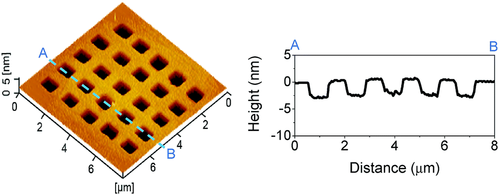 | ||
| Fig. 2 Nondestructive array of nanochannels fabricated on an H-passivated Si(100) surface. The normal load is 3 μN, and the number of area-sliding cycles is 2 during the sliding process. | ||
Effects of normal load and number of sliding cycles on fabrication depth and width
In the proposed straightforward and maskless nanofabrication method, the main fabrication factors for deciding fabrication depth and width are normal load and number of sliding cycles. Fig. 3a shows the AFM images of nanochannels fabricated by a SiO2 tip with radius of ∼1 μm under various normal loads of 0.5, 1, 2, and 3 μN under the following conditions: RH = 50%, and number of sliding cycles N = 100. The curves of the fabrication depth and width (full width at half maximum depth) versus the normal load are separately plotted in Fig. 4a. The figure indicates that both nanochannel depth and width increase with increasing normal load. These results also suggest that mechanical interaction can intensify tribochemical reaction to prompt material loss, which ultimately increases nanochannel depth and width.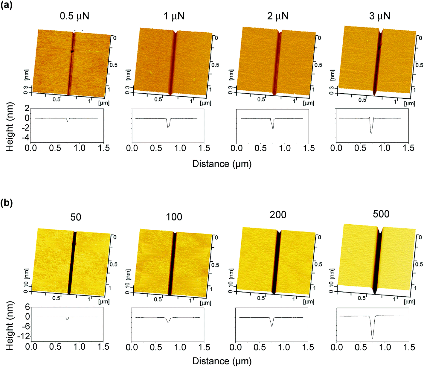 | ||
| Fig. 3 (a) Tribochemistry-induced direct nanofabrication under various normal loads. The number of sliding cycles during the sliding process is 100. (b) Tribochemistry-induced direct nanofabrication under various numbers of sliding cycles. The normal load during the sliding process is 3 μN. | ||
 | ||
| Fig. 4 (a) Fabrication depth and width vs. normal load. (b) Fabrication depth and width vs. number of sliding cycles. | ||
Fig. 3b shows the AFM images of the fabricated nanochannels at various N of 50, 100, 200, and 500 by a SiO2 tip with radius of ∼1 μm under the following conditions: RH = 50% and normal load Fn = 3 μN. Fabrication depth and width (full width at half maximum depth) versus the number of sliding cycles curves are shown in Fig. 4b. Fabrication depth increases linearly with the number of sliding cycles, which implies that nanochannel depth can be effectively controlled by adjusting the number of sliding cycles. Moreover, this result suggests that fabrication depth can continually increase without limit as long as the number of sliding cycles is increased, and thus, nanochannels with considerable depth can be produced. Fabrication width exhibits a slight increase with increasing number of sliding cycles, which is partly attributed to the slight drifting of the contact position between the SiO2 tip and the sample. When the number of sliding cycles increases from 100 to 500, the aspect ratio (depth-to-width ratio) of the nanochannel increases by nearly five times, which indicates that the aspect ratio of the nanochannel can be improved by increasing the number of sliding cycles when the normal load is kept constant.
Nanofabrication on Si(100), Si(110), and Si(111)
Given the anisotropic etching property of monocrystalline silicon in alkaline solution,23 fabricating nondestructive and shaping well-defined nanochannels on Si(111) surface is difficult when using friction-induced selective etching methods. However, unlike friction-induced selective etching methods, the proposed tribochemistry-induced direct nanofabrication method can directly obtain nondestructive nanostructures on the arbitrary crystal planes of monocrystalline silicon. As shown in Fig. 5, three nondestructive nanochannels with depths of approximately 1.4, 2.4, and 4 nm were separately fabricated by a SiO2 tip with radius of ∼1 μm on three typical crystal planes, i.e., Si(100), Si(110), and Si(111), under the same fabrication conditions, as follows: RH = 50%, Fn = 3 μN, and N = 100. The nanochannels produced on different crystal planes vary in depth under the same fabrication conditions.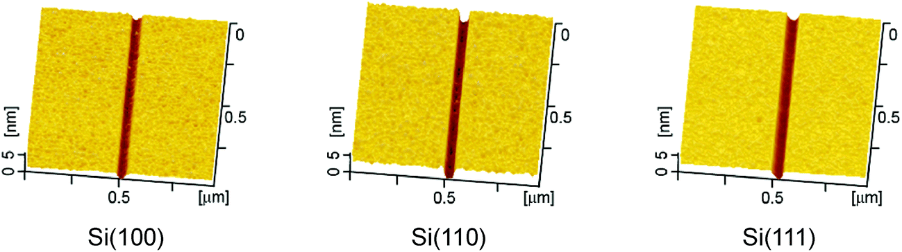 | ||
| Fig. 5 Fabrication of nondestructive nanochannels on different crystal planes of monocrystalline silicon. The normal load is 3 μN, and the number of sliding cycles is 100. | ||
SiO2 tip before and after fabrication
When the tribochemistry-induced direct fabrication method is used, the patterned feature of the nanochannel is mainly dependent on the applied normal load, the scanning trace, and the shape of the SiO2 tip. Both the normal load and the scanning trace can be accurately controlled by AFM. Given that contact pressure during fabrication is low, no obvious shape change in the SiO2 tip is speculated to occur after fabrication. Fig. 6a and b respectively show the AFM 3D topographies of the spherical SiO2 tip with ∼1 μm in radius before and after tribochemistry-induced direct fabrication under the following conditions: RH = 50%, Fn = 3 μN, and N = 15000. The corresponding cross sections of the SiO2 tip before and after fabrication are plotted in Fig. 6c for comparison. The observed small particle (Fig. 6b and c) on the surface of the SiO2 tip results from the tribochemistry-induced material removal of the silicon surface but not from the wear of the SiO2 tip. This result suggests that even after a lot of repeated fabrications, the SiO2 tip will not be worn and will nearly keep its original shape. Therefore, the SiO2 tip has a high working life span and the nanochannels fabricated under the same fabrication conditions can exhibit good uniformity.
 | ||
| Fig. 6 AFM images and profiles of the spherical SiO2 tip before and after tribochemistry-induced fabrication. (a) AFM image before fabrication. (b) AFM image after fabrication under the following conditions: Fn = 3 μN, and N = 15000. (c) Cross-sectional profiles of the SiO2 tip before and after fabrication. | ||
Resolution and limits of fabrication
When we fabricate nanochannels with a SiO2 tip, depth of the nanochannel is mainly dependent on the applied normal load and number of sliding cycles. The minimum depth achievable in our experiments was below 1 nm. Width of the nanochannel is generally relied on the real contact area of SiO2 tip and silicon. The best resolution of width was ∼30 nm. For example, a ∼0.7 nm deep and ∼30 nm wide (full width at half maximum depth) nanochannel (characterized by AFM) was obtained on an H-passivated Si(100) surface by using the proposed fabrication method, under the following condition: the radius of the SiO2 tip R ≈ 600 nm, RH = 50%, Fn = 1 μN, and N = 10. Given that the depth of nanochannel is near atomic-scale, at which the cross-sectional sample for TEM observation is difficult to be well prepared, such low a depth could not be clearly observed in the XTEM image. If we used a SiO2 tip with a smaller size, or decreased the normal load, the width of the nanochannel could be further decreased, and the minimum fabrication depth is expected to reach atomic-scale.Given that the tribochemical reaction is hard to take place under an ultralow-humidity environment with too less water molecules, the tribochemistry-induced direct fabrication is confining under such circumstance. Previous study suggested that the suitable relative humidity for producing appreciable nano-trenches on Si(100) surface should be higher than 10%.26,28 It was estimated that the effect of humidity on the tribochemistry-induced direct nanofabrication on an H-passivated Si(100) sample (without the native oxide layer covered on its surface) was different from that on a Si(100) surface. Hence, further experiments are necessary to investigate such effect. In addition, because the nanochannels were all obtained by sliding a single SiO2 tip with an AFM in our experiment, the fabrication area, as well as the efficiency was limited. Therefore, the present technique is not mass-productive. Development of multi-probe fabrication technique and large-area fabricating machinery for tribochemistry-induced direct fabrication provides a possibility to realize the mass-production.
Conclusion
Nondestructive nanochannels can be directly fabricated on the arbitrary crystal planes of monocrystalline silicon without masking or etching process by sliding the SiO2 tip under low contact pressure in humid air. Fabrication depth increases with increasing normal load and number of sliding cycles. Given that contact pressure is considerably lower than the hardness and the critical contact pressure for the initial yield of silicon, the sliding process does not result in silicon yield. HRTEM shows no lattice distortion beneath the nanochannels, which demonstrates that tribochemical reaction is responsible for the material removal of monocrystalline silicon. During fabrication, no appreciable wear can be observed on the surface of the SiO2 tip; hence, the working life span of the SiO2 tip and the fabrication uniformity of the nanochannels are high. As a maskless, straightforward, and crystal plane-independent nanofabrication method, the proposed tribochemistry-induced direct nanofabrication provides a new strategy to produce nondestructive silicon nanostructures, such as nondestructive nanochannels.Acknowledgements
The authors would like to acknowledge the financial supports from National Natural Science Foundation of China (91323302, 51375409 and 51305365).References
- A. D. Stroock, S. K. W. Dertinger, A. Ajdari, I. Mezić, H. A. Stone and G. M. Whitesides, Science, 2002, 295, 647–651 CrossRef CAS PubMed.
- L. D. Menard and J. M. Ramsey, Anal. Chem., 2013, 85, 1146–1153 CrossRef CAS PubMed.
- J. M. Perry, K. Zhou, Z. D. Harms and S. C. Jacobson, ACS Nano, 2010, 4, 3897–3902 CrossRef CAS PubMed.
- P. M. Sinha, G. Valco, S. Sharma, X. W. Liu and M. Ferrari, Nanotechnology, 2004, 15, 585–589 CrossRef.
- B. Z. Cvetkovic, O. Lade, L. Marra, V. Arima, R. Rinaldi and P. S. Dittrich, RSC Adv., 2012, 2, 11117–11122 RSC.
- H. Cao, Z. Yu, J. Wang, J. O. Tegenfeldt, R. H. Austin, E. Chen, W. Wu and S. Y. Chou, Appl. Phys. Lett., 2002, 81, 174–176 CrossRef CAS.
- H. Cho, J. Park, H. Park, X. Cheng, B. J. Kim and A. Han, Microfluid. Nanofluid., 2010, 9, 163–170 CrossRef.
- L. D. Menard and J. M. Ramsey, Nano Lett., 2011, 11, 512–517 CrossRef CAS PubMed.
- Y. Xu and N. Matsumoto, RSC Adv., 2015, 5, 50638–50643 RSC.
- M. Fouad, M. Yavuz and B. Cui, J. Vac. Sci. Technol., B: Microelectron. Nanometer Struct.--Process., Meas., Phenom., 2010, 28, C6I11–C6I13 CrossRef CAS.
- M. K. Bhuyan, F. Courvoisier, P. A. Lacourt, M. Jacquot, R. Salut, L. Furfaro and J. M. Dudley, Appl. Phys. Lett., 2010, 97, 081102 CrossRef.
- G. Spoldi, S. Beuer, M. Rommel, V. Yanev, A. J. Bauer and H. Ryssel, Microelectron. Eng., 2009, 86, 548–551 CrossRef CAS.
- Y. D. Yan, Y. Q. Geng, Z. J. Hu, X. S. Zhao, B. W. Yu and Q. Zhang, Nanoscale Res. Lett., 2014, 9, 212 CrossRef PubMed.
- B. W. Yu, Y. Q. Geng, Y. D. Yan and Z. J. Hu, Micro Nano Lett., 2014, 9, 707–711 Search PubMed.
- Z. Q. Wang, N. D. Jiao, S. Tung and Z. L. Dong, Appl. Surf. Sci., 2011, 257, 3627–3631 CrossRef CAS.
- Z. Q. Wang, N. D. Jiao, S. Tung and Z. L. Dong, Chin. Sci. Bull., 2010, 55, 3466–3471 CrossRef CAS.
- L. Zhang and J. Dong, Nanotechnology, 2012, 23, 085303 CrossRef PubMed.
- N. Kawasegi, N. Takano, D. Oka, N. Morita, S. Yamada, K. Kanda, S. Takano, T. Obata and K. Ashida, J. Manuf. Sci. Eng., 2005, 128, 723–729 CrossRef.
- T. Ogino, S. Nishimura and J.-i. Shirakashi, Jpn. J. Appl. Phys., 2008, 47, 712–714 CrossRef CAS.
- P. J. Zanzucchi and M. T. Duffy, Appl. Opt., 1978, 17, 3477–3481 CrossRef CAS.
- B. J. Yu, X. Y. Li, H. S. Dong and L. M. Qian, Micro Nano Lett., 2012, 7, 1270–1273 CAS.
- J. Guo, B. J. Yu, X. D. Wang and L. M. Qian, Nanoscale Res. Lett., 2014, 9, 241 CrossRef.
- H. Seidel, L. Csepregi, A. Heuberger and H. Baumgartel, J. Electrochem. Soc., 1990, 137, 3612–3626 CrossRef CAS.
- H. T. Lee, J. S. Oh, S. J. Park, K. H. Park, J. S. Ha, H. J. Yoo and J. Y. Koo, J. Vac. Sci. Technol., A, 1997, 15, 1451–1454 CAS.
- B. J. Yu, H. S. Dong, L. M. Qian, Y. F. Chen, J. X. Yu and Z. R. Zhou, Nanotechnology, 2009, 20, 465303 CrossRef PubMed.
- J. X. Yu, S. H. Kim, B. J. Yu, L. M. Qian and Z. R. Zhou, ACS Appl. Mater. Interfaces, 2012, 4, 1585–1593 CAS.
- F. Katsuki, J. Mater. Res., 2009, 24, 173–178 CrossRef CAS.
- X. D. Wang, S. H. Kim, C. Chen, L. Chen, H. T. He and L. M. Qian, ACS Appl. Mater. Interfaces, 2015, 7, 14785–14792 CAS.
- L. Chen, S. H. Kim, X. D. Wang and L. M. Qian, Friction, 2013, 1, 81–91 CrossRef.
- A. L. Barnette, D. B. Asay, D. Kim, B. D. Guyer, H. Lim, M. J. Janik and S. H. Kim, Langmuir, 2009, 25, 13052–13061 CrossRef CAS PubMed.
- X. S. Feng, Y. K. Ren and H. Y. Jiang, Biomicrofluidics, 2013, 7, 054121 CrossRef PubMed.
| This journal is © The Royal Society of Chemistry 2015 |