
 Open Access Article
 This Open Access Article is licensed under a Creative Commons Attribution-Non Commercial 3.0 Unported Licence
Synthesis, optical properties, and photochemical activity of zinc-indium-sulfide nanoplates†
Björn
Kempken
a,
Volodymyr
Dzhagan
bc,
Dietrich R. T.
Zahn
b,
Marcelo J. P.
Alcocer
d,
Ilka
Kriegel‡
d,
Francesco
Scotognella
d,
Jürgen
Parisi
a and
Joanna
Kolny-Olesiak
*a
aEnergy and Semiconductor Research Laboratory, Department of Physics, Carl von Ossietzky University of Oldenburg, 26111 Oldenburg, Germany. E-mail: joanna.kolny@uni-oldenburg.de
bSemiconductor Physics, Technische Universität Chemnitz, Reichenhainer Straβe 70, 09107 Chemnitz, Germany
cV. E. Lashkaryov Institute of Semiconductors Physics, National Academy of Sciences of Ukraine, Kyiv, 03028, Ukraine
dDipartimento di Fisica, Politecnico di Milano, Piazza Leonardo da Vinci 32, 20133 Milano, Italy
First published on 12th October 2015
Abstract
Zinc indium sulfide is an interesting material for photocatalytical applications. Here, ZnxIn2S3+x nanoplates with varying value of x (between 0 and 1) were synthesized by means of colloidal chemistry. The nanoplates have a diameter of up to 100 nm and a relatively small thickness of 2.5 nm. The structure of the Zn-free particles could be assigned to β-In2S3 based on the powder X-ray diffraction and Raman spectroscopy data. Particles containing Zn exhibit the hexagonal ZnIn2S4 structure. The samples were studied by steady state and time resolved photoluminescence spectroscopy. Our results demonstrate that increasing amounts of Zn incorporation result in more intra-gap states that participate in radiative sub-band gap recombination and simultaneously decrease non-radiative defect states that might, for example, originate from vacancies in the structure. Furthermore, the nanoplates exhibit significantly increased photochemical activity in the degradation of rhodamine 6G, depending on their Zn content. The high surface-to-volume ratio and the intra-gap states might be responsible for this finding.
Introduction
Nanoscaled semiconducting materials are of great interest in the field of materials science because of their size and shape dependent optical, electronic, and catalytic properties.1–4 In particular, materials such as cadmium and lead chalcogenides have been extensively studied during the past two decades.2,5,6 In spite of their interesting properties, their potential for large scale application is limited, due to the toxicity of cadmium and lead. Therefore, ternary and quaternary materials such as copper, indium, zinc, or tin-based semiconductors are attracting scientific attention as possible alternatives.7–12One such alternative material is ZnIn2S4, which is a direct semiconductor with bandgap energies reported for different size and shape of nanostructured particles lying between 2.2 and 2.8 eV.13 ZnIn2S4 can crystallize in two polymorphs based on cubic and hexagonal lattices. The cubic polymorph has interesting thermoelectrical properties,14 while the hexagonal modification exhibits photoluminescence and photoconductivity. Both polymorphs are photocatalytically active materials.13,15–20 Nanoribbons, nanotubes, and microspheres of hexagonal ZnIn2S4 have been synthesized in a solvothermal reaction,21 while nanowires could be obtained by using a porous polycarbonate membrane as hard template.20 Nanoparticles with a size between 2.1 and 9.2 nm and large, aggregated nanoplates were obtained by means of colloidal chemistry.19 Also other zinc-indium-sulfide microspheres with the general stoichiometry ZnxIn2S3+x (x ≥ 1) were synthesized by a solvothermal method, and their photocatalytic activity in water splitting reaction has been tested.22 However, there are no reports about the formation of well-defined ZnxIn2S3+x nanoplates.
In this article, we present the colloidal synthesis of ultrathin, hexagonal ZnxIn2S3+x nanoplates (with 0 ≤ x ≤ 1) and show their capability to act as photocatalysts for the degradation of organic dyes. The nanoplates were synthesized using different amounts of zinc, and their composition dependent structure, optical properties, and photocatalytic activity were studied.
Experimental section
Materials
Indium(III)acetate (99.99% – In) (InAc3), copper(I)acetate (99.99% – Cu) (CuAc), zinc(II)acetate (99.99% – Zn) (ZnAc2), oleylamine (OLAM), oleic acid (90%, technical grade) (OA), 1-dodecanethiol (1-DDT), and tert-dodecanethiol (t-DDT) were purchased from Sigma Aldrich. All the chemicals were used without further purification.Preparation of Cu-stock solution
1 mmol CuAc was dissolved in 10 mL OLAM and heated under stirring and inert gas up to 100 °C for 10 min. The solution was stored under argon.Synthesis of the nanoplates
In a typical synthesis, 1 mmol InAc3, 100 μL Cu-stock solution, 1 mmol ZnAc2, 10 mL OLAM, and 2 mL OA were loaded in a three-neck-flask and stirred under vacuum at room temperature for 15 min. Subsequently, the reaction solution was heated up to 280 °C under nitrogen atmosphere. At this temperature, a mixture of 0.25 mL 1-DDT and 2.5 mL t-DDT was rapidly injected. After additional 60 min, the solution was cooled down to room temperature, and the resulting nanoplates were isolated from the by-products of the reaction and the remaining starting materials by precipitation with ethanol and subsequent redissolution in hexane; the latter was repeated up to five times. Afterwards, the purified nanoplates were dissolved in chlorobenzene.Degradation of rhodamine 6G
2 mL rhodamine 6G solution (100 μmol L−1) was added to 1 mL nanoplates solution (1 mg mL−1). The resulting solution was illuminated with UV light (365 nm) for a total time of 10 min. Absorption spectra were taken at different irradiation intervals (between 10 s and 10 min), in order to monitor the decomposition of the dye.Characterization
Transmission electron microscopy (TEM) images were taken on a Zeiss EM902A electron microscope using an 80 kV electron source. Samples were prepared from a hexane solution on a carbon coated copper grid and dried under air for 24 hours. High resolution transmission electron microscopy (HRTEM) observations as well as energy dispersive X-ray spectroscopy (EDX) measurements were performed on a JEOL JEM2100F electron microscope equipped with an X-Max80 SDD-detector. UV/vis-absorption spectra were taken on a Varian Carry 100 scan spectrophotometer, and samples were prepared by diluting a 5–50 μL nanocrystal solution with 3 mL n-hexane. PL spectra were taken on a Fluorolog 3. Powder X-ray diffraction (XRD) was measured with a PANalytical X'Pert PRO MPD diffractometer using Cu Kα radiation (1.54 Å), standard Bragg–Brentano θ–2θ geometry, and variable slits. The samples were measured on low background silicon sample holders and prepared by dropping colloidal solution on the holder and letting the solvent evaporate (by heating to 70 °C for 30 min). Raman spectra were excited with the 514.7 nm line of diode pumped solid state (DPSS) laser (Cobolt) or a 325 nm line He–Cd laser and registered with an HR LabRam spectrometer, equipped with a liquid nitrogen cooled charge-coupled device (CCD) detector, at a spectral resolution of 5 cm−1. The incident laser power was kept below 0.02 mW, in order to avoid sample heating under the microscope objective (100× and 40× for 514.7 nm and 325 nm excitation, respectively). Time-resolved photoluminescence measurements were performed using a femtosecond laser source and streak camera detection system. An unamplified Ti:sapphire laser (Coherent Chameleon Ultra II) operating at 80 MHz was tuned to provide pulses with central wavelengths of 800 nm, energies of ∼50 nJ, and temporal and spectral bandwidths of ∼140 fs and ∼5 nm, respectively. An acousto-optical modulating pulse picker (APE Pulse Select) was used to reduce the repetition rate to 2 MHz to accommodate the long decay times of the samples. A β-barium borate crystal provided type I phase-matched second harmonic generation, leading to pulses with central wavelengths of 400 nm. These were focused onto the sample, maintaining a low fluence (<30 mJ cm−2, ∼100 μm spot diameter) in order to avoid any saturation effects in the sample. The resulting collected emission was analyzed by a spectrograph (Princeton Instruments Acton SP2300) coupled to a streak camera (Hamamatsu C5680) equipped with a linear voltage sweep module. In this way, measurements of photoluminescence intensity as a function of both wavelength and time were obtained with spectral and temporal resolutions of ∼1 nm and ∼0.5 ns respectively. Temporal broadening of the pump pulses caused by dispersive elements was confirmed to be well below the response time of the detection system.Results and discussion
The photocatalytic activity of nanostructured materials depends on their electronic properties and the characteristics of their surface. This study concentrates on the synthesis and characterization of nanocrystalline ZnxIn2S3+x with high specific surface area and variable composition. The manuscript is organized in the following manner: in the first part we describe the synthesis of the ZnxIn2S3+x nanoplates, and then we present their detailed structural and spectroscopic characterization. We conclude with the demonstration of the photochemical activity of the synthesized nanoplates in the decomposition of rhodamine G6.Colloidal synthesis of zinc indium sulfide nanoplates
The starting materials for the formation of ZnxIn2S3+x nanoplates are zinc and indium acetate. The source of sulfur is tert-dodecanethiol, a compound that can be easily decomposed thermally and provides the reaction solution with sulfur monomers. Therefore, it has been used as a sulfur source in the synthesis of metal sulfides, such as CuInS2, Cu2−xS, or Cu3SnS4 nanoparticles (NPs).23–27 1-Dodecanethiol and oleic acid act as stabilizers, which not only provide the emerging particles with colloidal stability, but also regulate the activity of the monomers in the reaction solution. The reaction takes place in oleylamine, which is a coordinating solvent and can also play a role of a stabilizer for the growing particles. A small amount of copper acetate (indium/copper ratio 100![[thin space (1/6-em)]](https://www.rsc.org/images/entities/char_2009.gif) :1) is present in the reaction solution, because it facilitates the formation of the nanoplates.
:1) is present in the reaction solution, because it facilitates the formation of the nanoplates.
The composition of the nanoplates depends on the amount of zinc used for the synthesis. When comparing the ratio of the starting materials to that of the elements comprising the nanoplates, only about 50% of the expected amount of zinc is incorporated into the nanoplates. The composition of the different samples, obtained by energy dispersive X-ray spectroscopy (EDX) measurements can be found in Table 1. By changing the amount of zinc in the reaction solution, we can tune the composition of the ZnxIn2S3+x nanoplates between x = 0 and x = 1. However, compared to the anticipated ZnxIn2S3+x stoichiometry, the sulfur content is larger than expected for all samples. This is most likely due to the presence of thiols on the surface of the particles. It has to be noted that we also detect a small amount of copper in all measurements; however, it is not possible to determine the exact concentration of copper ions in the samples, as this element is always also present as a background signal. Due to the small concentration of copper ions in the samples, subtraction of the background values does not give reliable results. Because the concentration of copper in all reaction solutions is the same, we can safely assume that it also does not vary significantly among all the samples studied, and we can attribute the differences observed between them to the variation of the Zn concentration.
| Sample | ZnAc2 in the reaction solution [g] | Zn/In ratio in the reaction solution | xZn | Ina | (3 + x)S |
|---|---|---|---|---|---|
| a The value for In was normalized to 2. | |||||
| ZIS250 | 0.250 g | 1.37:1 |
1.05 | 2 | 5.94 |
| ZIS150 | 0.150 | 0.85:1 |
0.79 | 2 | 5.10 |
| ZIS100 | 0.100 g | 0.57:1 |
0.61 | 2 | 4.55 |
| ZIS50 | 0.050 g | 0.27:1 |
0.30 | 2 | 4.31 |
| ZIS25 | 0.025 g | 0.14:1 |
0.18 | 2 | 3.82 |
| ZIS13 | 0.0125 g | 0.07:1 |
0.09 | 2 | 3.71 |
| ZIS0 | 0.00 g | 0.00:1 |
0 | 2 | 3.49 |
Structural characterization of zinc indium sulfide nanoplates
Fig. 1 shows transmission electron microscopy (TEM) images of the nanocrystals obtained by our synthetic procedure. The particles are thin nanoplates with a diameter up to 100 nm independent of the amount of zinc used for the synthesis. Many of them have regular, hexagonal or triangular shapes with 120° or 60° angles, respectively (Fig. 1b and S1 of the ESI†). Others have irregular shapes, with torn away edges, which we attribute to their low mechanical stability during the vigorous stirring process and the precipitation, centrifugation and redissolution steps during the cleaning procedure (Fig. 1a). Most nanoplates are located flat on the TEM grid, however, in some larger aggregates, bundles of several plates lying on the edge could be found (Fig. 1c–e), allowing their thickness to be determined at 2.5 nm. This is close to the value of the c-axis of hexagonal ZnIn2S4 (ICDD 03-065-2023), which is 2.4 nm. This crystallographic structure is composed of a repeating unit of 4 layers of densely packed sulfur ions of 1.2 nm thickness with one layer of Zn ions in the tetrahedral voids, one layer of In ions in octahedral voids, and one layer of In ions in tetrahedral voids. This should result in a relatively low contrast in high resolution transmission electron microscopy (HRTEM) images of single nanoplates lying flat on the substrate and in a strong broadening of powder X-ray diffraction (XRD) reflections corresponding to (00l) lattice planes.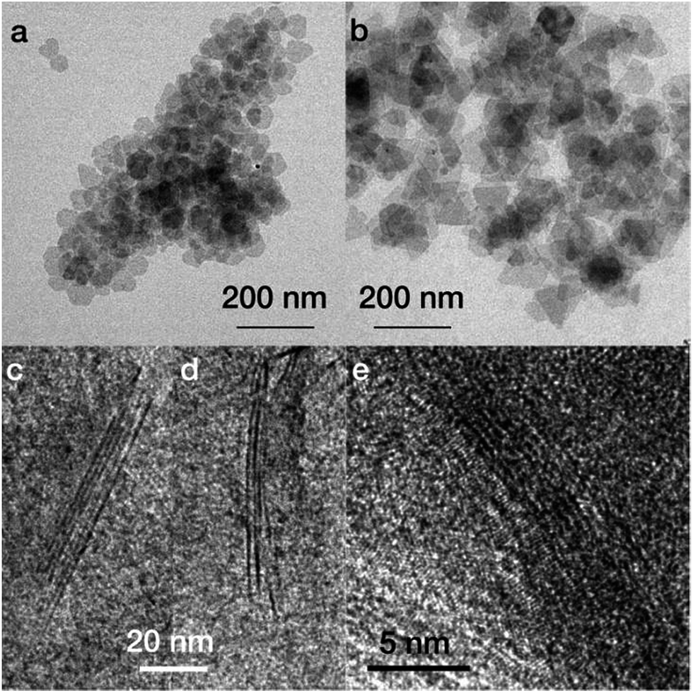 | ||
| Fig. 1 Overview TEM images of the nanoplates after five precipitation and dissolution steps (a) and without any cleaning procedure (b). TEM images of nanoplates lying on the edge (c–e). | ||
Fig. 2 shows the XRD patterns of the products for different Zn contents. The position of the reflections and their relative intensities are independent of the particle's composition. A similar behavior was reported previously for ZnxIn2S3+x particles, which showed comparable profiles of their diffraction patterns in spite of their differing compositions (x = 1 to 5).22
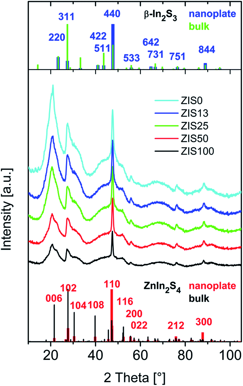 | ||
| Fig. 2 XRD patterns of nanoplates obtained with different Zn amounts in the reaction solution. The reference patterns are ICDD 01-084-1385 for In2S3 (top panel, green) and ICDD 03-065-2023 for ZnIn2S4 (bottom panel, black). The intensity of the blue (top panel) and red (bottom panel) pattern was estimated for nanoplates with a diameter of 30 nm and thickness of 2.4 nm, with a growth direction perpendicular to the 〈111〉 direction of In2S3 and 〈001〉 direction of ZnIn2S4, respectively. | ||
Notably, in our case, the observed intensities of the measured reflections substantially differ from those of the typical reference patterns (ICDD 01-084-1385 for β-In2S3, Fig. 2, top panel, green pattern and ICDD 03-065-2023 for ZnIn2S4, bottom panel, black pattern). This deviation from the intensity values of the bulk reference patterns and the pronounced broadening of some reflections result from the anisotropic growth of the particles. In order to compare the reference patterns with the measured data, we have to take into account the shape of the nanocrystals.
As a rough estimate of the changes expected in the intensity (bulk vs. thin nanoplate), we calculated the number of lattice planes present in a nanoplate of 2.4 nm thickness and a diameter of 30 nm for each reflection of the reference pattern (black and green sticks in Fig. 2). We assumed a growth perpendicular to the 〈001〉 and 〈111〉 direction for the hexagonal ZnIn2S4 and for the cubic β-In2S3, respectively. The numbers obtained from this calculation were used to weigh the intensity values of the reference patterns. The resulting values are shown as red and blue bars in Fig. 2. Both patterns are in good agreement with the experimental data. Only in the region of about 20° 2θ, we see a discrepancy between the calculated and the measured pattern. We observe in all samples a broad signal centered around 20° 2θ with varying intensity (depending, e.g., on the number of cleaning steps). We do not find reflections in this region in the reference pattern of β-In2S3. Furthermore, based on our estimated intensity values, we do not expect a strong reflection stemming from ZnIn2S4 here, because it would correspond to (006) lattice planes, which are perpendicular to the short axis of the nanoplates. Thus, we assign it to ligand molecules, either bound to the surface of the nanoplates, or present as impurities in the samples. The lattice spacing for this peak calculated with the Bragg equation is 0.43 nm, which corresponds to the closest possible distance between two carbon chains. Usually, the occurrence of this kind of signal indicates the presence of excess organic molecules, which were not sufficiently removed during the cleaning procedure.28 However, in the case of the nanoplates, we expect ligands on their surface to form a locally ordered layer. Therefore, we assign the reflection at 20°, at least partly, to the presence of the highly ordered ligand shell on the nanoplate's surface.
Taken together, the comparison of the measured and calculated intensity of the diffraction patterns confirms our assignment of the preferential growth direction of the nanoplates to be the 〈001〉 and 〈111〉 direction for the hexagonal ZnIn2S4 and for the cubic β-In2S3, respectively. However, the pronounced broadening of most of the reflections, results in relatively similar diffraction patterns for nanoplates with hexagonal ZnIn2S4 and cubic β-In2S3 structure. Therefore it is not possible to unambiguously assign the crystallographic structure of the nanoplates with varying Zn content, based only on the XRD data.
Additional information about the internal structure of the ZnxIn2S3+x (ZIS) nanoplates grown at different Zn concentrations in the parental solution can be gained from their lattice vibration spectra obtained by means of Raman spectroscopy. Raman spectra excited with λexc = 325.0 nm and 514.7 nm are shown in Fig. 3. Based on the UV-vis spectra (see below in the section “Optical properties”), the higher energy excitation is resonant for the samples containing Zn (Fig. 3a), while 514.7 nm provides resonance condition for exciting the vibrational Raman spectrum of the sample without Zn, i.e., InxSy (Fig. 3b). Under 325 nm excitation, a broad scattering feature is observed in the spectrum with several distinct peaks, which increases in intensity as the amount of ZnAc2 in the reaction solution increases from 0.05 g up to 0.25 g (Fig. 3a). The spectrum of the nanoplates synthesized at the highest nominal Zn content (0.25 g) correlates well with the Raman spectrum of bulk29 and microcrystalline22 ZnIn2S4, reported previously. The most pronounced Raman band in Zn-containing samples peaks near 345 cm−1 under λexc = 325 nm and is close in frequency to the Fu1(LO) mode of the ZnIn2S4 lattice.29 According to theory, this mode should not be Raman active, but its observation in bulk crystals has been explained as a breaking of selection rules due to defects.29 In our case, the internal non-stoichiometry of the nanoplates and especially their large surface-to-volume ratio might be the reason for activating forbidden Raman mode(s). Moreover, we observed an important role of defects and intra-gap states in our ZIS nanoplates (see the discussion in section “Optical properties”). The high surface-to-volume ratio of our nanoplates accounts for the observed broadening of the phonon bands.30,31 According to previous observations for other semiconductor NPs, the surface-induced broadening alone can make up as much as 30–50% of the Raman peak width.32 Additionally, the effect of phonon confinement is known to cause broadening and a shift of the optical phonon peaks (usually to lower frequencies as compared to bulk resonance) for semiconductor NPs smaller than 10 nm such as ours.33–35 According to other works on ZnIn2S4,36,37 Raman modes at 254 and 345 cm−1 stem mainly from vibrations of S atoms. An alternative origin of the 345 cm−1 Raman mode in the spectra of our ZnIn2S4 nanoplates could be nanosized ZnS inclusions, because the main resonant Raman peak of small ZnS crystallites occurs in the range of 345–350 cm−1 and is due to longitudinal optical (LO) vibrations.38 However, at the resonant excitation of II–VI nanocrystals (λexc = 325 nm for ZnS), also a second order peak (2LO) at approximately double the frequency is usually observed,38 even in alloys39 and ultrasmall crystallites (<2 nm).40 The latter proves to be an efficient way of determining ZnS precipitations in multicomponent crystals, for example Cu2ZnSnS4.38 For the ZnIn2S4 nanoplates studied here no feature is observed near 700 cm−1 (Fig. 3a) indicating the absence of ZnS nano-inclusions. Moreover, no ZnS NPs were detected in these samples by TEM.
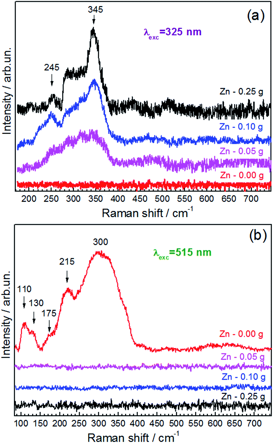 | ||
| Fig. 3 Raman spectra of the nanoplates samples with different Zn concentration, recorded using λexc = 325 nm (a) and 514.7 nm (b). The features discussed in the text are marked by arrows. | ||
The most efficient resonant excitation is the near-bandgap one, which explains the absence of any Raman features for the sample without Zn at λexc = 325 nm (Fig. 3a) and the strong Raman scattering intensity at λexc = 514.7 nm (Fig. 3b). It contains an intense and relatively broad band at 300 cm−1 and weaker and narrower ones at 110, 130, 175 and 215 cm−1. These features do not match the strongest Raman bands of In2S3 (246 and 365 cm−1)41 or InS (150 cm−1).42 The main Raman-active vibration of the most stable relevant oxide, In2O3, occurs at about 290 cm−1,41 but it cannot explain the rather strong and extremely broad structured feature observed for our InxSy nanoplates (Fig. 3b). The latter obviously results from an overlap of several vibrational modes. Based on the atomic ratio of In:S being near 2:3 (Table 1) and by taking into account the thickness of our nanoplates of only 2.5 nm, the spectrum of our InxSy nanoplates can be assigned to the In2S3 features broadened and shifted by the phonon confinement and surface effect, as explained above.
Fig. 4a shows an HRTEM image of a nanoplate. The corresponding fast Fourier transform (FFT) pattern (Fig. 4b) indicates that the entire nanoplate is mono-crystalline and grows in the ab plane of the hexagonal ZnIn2S4 structure. Our findings are in good agreement with the XRD data, exhibiting a pronounced and narrow (110) reflection with missing reflections corresponding to (002) and (004) planes of ZnIn2S4 (Fig. 2). This is exactly what we expect for thin nanoplates growing in the ab plane. While the lattice planes can hardly be seen in isolated nanoplates because of their low thickness, moiré fringes are observed when nanoplates overlap, which further confirms the mono-crystalline nature of the nanoplates. Fig. 4c shows such a moiré pattern with hexagonal symmetry, resulting from two overlapping nanoplates rotated by 2° with respect to each other. In the FFT of this region (Fig. 4d), the patterns confirm a 2° rotation of the nanoplates. A hexagonal pattern in the center of the FFT reflects the symmetry of the moiré fringes and their spacing of 5 nm.
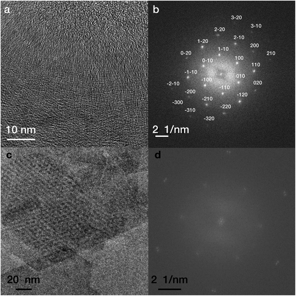 | ||
| Fig. 4 HRTEM image of a single nanoplate (a) and the corresponding FFT (b), which can be indexed to the hexagonal ZnIn2S4 viewed along the 〈001〉 zone axis. TEM image of overlaying nanoplates exhibiting a moiré pattern (c), and an FFT of this region (d). | ||
Optical properties
A careful investigation of the effect of composition on the optical properties of three samples of ZIS nanoplates with increasing Zn content was performed through multiple optical spectroscopic measurements, such as continuous wave (CW) absorption and photoluminescence (PL) as well as time resolved (TR) PL measurements. In the CW absorption analysis we observe a steep absorption onset around 3 eV (413 nm) for all samples with a weak absorption extending to the red (Fig. 5). The Tauc's plot,43i.e., absorbance squared versus energy, gives a linear relationship, which corresponds to a direct transition (see ESI Fig. S2†). The extrapolation of the linear trend to the energy axis determines the band gap. Due to a large contribution from scattering, a precise analysis of band gap shifts with changing composition is not possible. Nevertheless, a direct transition at around 3 eV can be extracted in all samples, relatively close to the bulk bandgap of ZnIn2S4 at 2.8 eV.44 In line with the recent publication by Chen et al.45 we expect a composition dependent bandgap, i.e., a blue shift with increasing incorporation of zinc over indium. Notably, a significant contribution to the absorption is observed below gap, which is largely due to scattering of the samples, however, a significant contribution might also correspond to defect states causing an Urbach tail extending into the forbidden gap.46 Indeed, in past investigations on ZnIn2S4 films, a density-of-state tail below the conduction band (CB) reaching into the forbidden gap was observed.46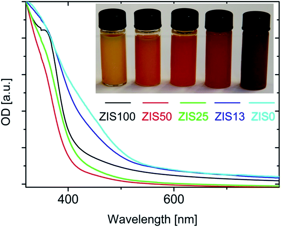 | ||
| Fig. 5 Normalized absorption spectra of nanoplates synthesized with different amount of ZnAc2 in the reaction solution (the kink in the black curve about 350 nm is an instrumental artifact). The inset shows a photograph of the corresponding solutions. | ||
To better understand this we performed CW PL measurements on the samples by exciting at 3.1 eV (400 nm – above band gap, blue curves in Fig. 6) and at 2.8 eV (450 nm – below band gap, red curves in Fig. 6). The resulting PL shows a relatively broad peak with a large Stokes shift. A blue shift of the PL as well as an increase in intensity with increasing content of Zn was found for both values of the excitation wavelength. This is visualized by the images of the sample cuvettes illuminated with a handheld UV-lamp (Fig. 6, inset). A careful analysis of the PL spectra allowed a fitting with one or two Gaussians. A common peak at around 2.1 eV (590 nm) in all Zn containing samples was found with rather low intensity that is increasing with the Zn content. For the two samples with the highest Zn content, an additional intense peak arises at 2.3 eV (540 nm) and 2.5 eV (496 nm), respectively. The excitation below band gap with 2.8 eV (450 nm) shows a similar trend, however, with a much lower intensity (factor of approximately five): a Gaussian peak at around 2.1 eV in each sample with low intensity and an additional peak for the two higher samples with the highest Zn content peaking at around 2.3 eV and 2.41 eV, respectively.
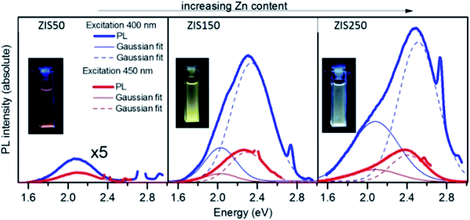 | ||
| Fig. 6 PL spectra for three samples with increasing Zn content (increasing from ZIS50, ZIS150, to ZIS250). Blue curves correspond to excitation at 400 nm, while red curves correspond to excitation at 450 nm. The thick solid curves represent the experimental data, and the thin solid and dotted curves the Gaussian fits. | ||
The large Stokes shift observed is indicative of radiative carrier recombination from intra-gap levels, or donor–acceptor pair recombination, and not from the transition between quantized energy levels in conduction and valence bands.47 Indeed, we do not observe any PL corresponding to the inter-gap recombination (at around 3 eV). Notably, the excitation with 450 nm, which is below the bandgap, results in similar PL behavior. The latter indicates the presence of absorption and subsequent emission from states below the band gap. This is in agreement with the Urbach tail observed in the absorption spectra.
The results of the PL measurements are interpreted in the following way: the electron excited from the valence band or from the acceptor levels to the conduction band (CB) thermalizes to and below the bottom of the CB. The electron then recombines with the hole, trapped at an acceptor. Due to the high defect density of ternary compounds based on Zn, In, and S, a manifold of intrinsic defects might be responsible for such donor and acceptor levels, e.g., Zn ions in the In sublattice, In ions in the Zn sublattice, and vacant sites in both Zn and In sublattices. These defects characterize the electronic properties of the material and give rise to a manifold of additional electronic levels. As such, numerous defect levels inside the forbidden energy gap are expected.44 Interestingly, in our work, we observe not only below gap emission, but two distinct contributions peaking at 2.1 and around 2.3–2.5 eV. Similar results were obtained by A. Serpi,44 who discusses the existence of a manifold of impurity levels in films of ZnIn2S4, as determined via photoconductivity measurements. Aside from the band gap peak, three other peaks at around 1.4 eV, 2.35 eV, and 2.55 eV were observed in the photoconductivity experiments. These reflect three impurity levels in the forbidden energy gap taking part in the photoconductivity process.44
Resolving PL emission temporally as well as spectrally can often yield further insight into the electronic structure and behavior of a material system. As such, TR PL measurements were performed at all four samples (ZIS250, ZIS150, ZIS50 and Zn-free ZIS0) with excitation at 3.1 eV (400 nm). In contrast to the CW PL, all samples – including the Zn-free ZIS0 – were seen to have some emission in TR measurements. This discrepancy can most likely be attributed to the higher excitation fluences and detection efficiency of the TR PL experimental setup with respect to the CW PL setup.
Inspection of the TR PL dynamics showed that they could be well described by either mono- (in the case of ZIS0) or bi-exponential decays with short and long decay constants of the order of 1 ns and 100 ns, respectively. These two emission components were, however, strongly spectrally overlapped, precluding further individual analysis based on spectral selection. As such, a global analysis approach was taken, with the entire TR PL map being fitted using the biexponential function,
 | (1) |
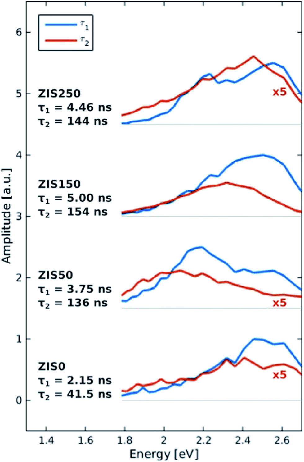 | ||
| Fig. 7 TR PL amplitude spectra. Each spectrum, Ai(ε), is associated with a mono-exponential decay of time constant τi, such that the TR PL signal, PL(ε,t), is given by the sum of the spectrum-decay product. Spectra have been scaled and offset for clarity. | ||
Whilst the Zn-free sample (ZIS0) shows a weak τ2 component with almost identical spectral shape to the τ1 component, the incorporation of Zn can be seen to increase the amplitude of the τ2 spectrum and change its shape. This shows that the short component is intrinsic intra-gap ZIS emission, whilst the long emission component can be associated to states arising from the presence of Zn. Given their extremely low energy (cf., band-gap ∼ 3 eV) and long lifetime, such states are likely to be deep intra-gap trap states arising from defect sites due the incorporation of Zn into the crystal lattice.
The peak of the τ2 spectrum can be seen to blue-shift with increasing Zn content, from circa 1.98 eV (625 nm) in ZIS50 to 2.43 eV (510 nm) in ZIS250. This is consistent with the blue-shift seen in CW PL, and indicates a reduced trap depth. Furthermore, the lifetime of both short and long emission components can be seen to increase marginally, suggesting a reduction in non-radiative decay channels. This can also be observed in the CW PL measurements (Fig. 6) as a significant increase in the PL quantum yield with increasing Zn content. Taken together, all these factors suggest that the increased incorporation of Zn into the lattice results in an improvement in crystal quality.
In summary, with increasing Zn incorporation, more intra-gap states are created. These participate not only in radiative sub-band gap recombination, but also simultaneously decrease non-radiative defect states that might, for example, originate from vacancies in the crystal structure.
Photochemical behavior of zinc indium sulfide nanoplates
The photochemical activity of ZIS nanoplates was evaluated by the degradation of rhodamine 6G (R6G) under UV light. R6G is a non-biodegradable and possibly carcinogenic48 organic dye of a remarkably high photostability, used, e.g., as gain medium in dye lasers or in paper, textile, or printing industry. Furthermore, it is a good model system for many other organic pollutants.ZIS was demonstrated previously to be a suitable photocatalyst for the degradation of organic dyes, among others R6G,13,15 therefore, we also used this reaction to evaluate the photochemical activity of our nanoplates. In Fig. 8, absorption spectra are shown, which were taken at different stages of the decomposition process of R6G in the presence of ZIS nanoplates under UV irradiation. The spectrum of R6G is dominated by an intense resonance at around 530 nm that decreases in intensity with reaction time. A pure R6G solution without the nanoplates remains stable under the same conditions, and no decrease in the concentration of the dye can be observed. During the degradation process of R6G, the absorption maximum of the dye shifts to shorter wavelengths, and an irradiation time of 10 min is sufficient to decompose the dye completely when Zn-rich nanoplates are used (Fig. 8a). The final absorption spectrum taken from this sample (600 s) does not exhibit any features typical of R6G. Thus, the degradation of R6G in the presence of our ZIS nanoplates is considerably faster as compared to results reported in literature, where photocatalytic experiments with ZIS microspheres were conducted on a time scale of several hours.16–19 We attribute this to the high specific surface area of ultrathin nanoplates used in our study.
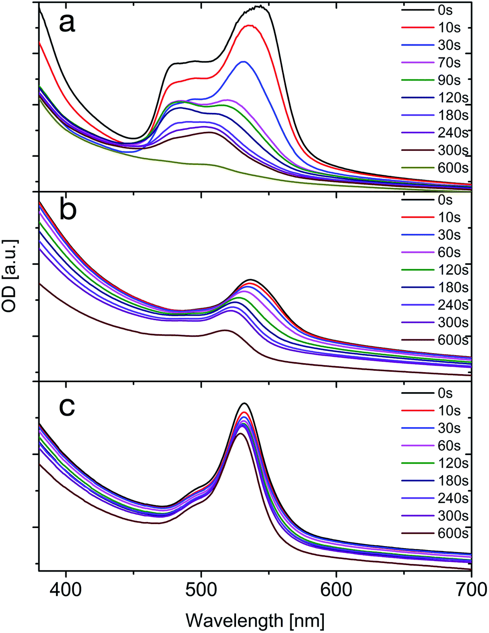 | ||
| Fig. 8 Absorption spectra taken at different times during decomposition of R6G with samples ZIS50 (a), ZIS25 (b), and ZIS13 (c). | ||
The decomposition of the dye is considerably slower when nanoplates with a smaller Zn content are used (Fig. 8b and c). We exclude a smaller number of photons available for photoexcitation to explain the observed behavior, as the absorption of Zn-rich nanoplates is blue shifted with respect to particles containing less zinc. Therefore, we conclude that the difference in the photochemical activity of the nanoplates results from different electronic or surface properties, depending on the composition of the particles. The formation of intra-gap states in the structure may also play a role here. As we have seen from our CW and TR PL results, the contribution of long lived intra-gap states increases with increasing amounts of Zn in the structure, simultaneously leading to an improvement in crystal quality, i.e., a removal of non-radiative defect states. A careful evaluation of the role of Zn incorporation, intra-gap formation, and defect states in the structure and, in particular, on the photocatalytic activity is ongoing. Furthermore, a correlation of the high surface-to-volume ratio on both should deliver a better understanding of the photocatalytic processes responsible for the highly increased photocatalytic activity of our ultrathin ZIS nanoplates.
Conclusions
We developed a synthesis for ultrathin, colloidal, single crystalline ZnxIn2S3+x nanoplates with varying Zn content between x = 0 and x = 1. The structure of the Zn-free particles was assigned to β-In2S3 based on the powder X-ray diffraction and Raman spectroscopy data. Particles containing Zn exhibit the hexagonal ZnIn2S4 structure. The formation of the nanoplates was facilitated by the presence of copper ions in the reaction solution, and their role in the growth process and the growth mechanism will be evaluated in further studies. The optical and photochemical properties of the nanoplates depend on their Zn content. A generally much higher photocatalytic activity for the degradation of rhodamine 6G was found for our ultrathin ZnxIn2S3+x nanoplates as compared to thicker ZnxIn2S3+x nanostructures. This might result from the unique shape of our nanoplates, which have a thickness of only 2.5 nm and a diameter of up to 100 nm, providing a high surface-to-volume ratio. Degradation was also seen to improve with increasing Zn content. We speculate that the formation of intra-gap states with increasing Zn content and the simultaneous decrease in non-radiative defect states might play a major role on the photocatalytic activity and deserves a further in depth evaluation.Acknowledgements
We gratefully acknowledge funding of the EWE Research Group “Thin Film Photovoltaics” by the EWE AG, Oldenburg. The authors acknowledge also the financial support by the MWN (Material World Network) Program between the National Science Foundation of the U.S. and the Deutsche Forschungsgemeinschaft (Grant No. Li 580/8-1).Notes and references
- A. R. Tao, S. Habas and P. Yang, Small, 2008, 4, 310–325 CrossRef CAS.
- C. Burda, X. Chen, R. Narayanan and M. a. El-Sayed, Chem. Rev., 2005, 105, 1025–1102 CrossRef CAS PubMed.
- C. B. Murray, C. R. Kagan and M. G. Bawendi, Annu. Rev. Mater. Sci., 2000, 30, 545–610 CrossRef CAS.
- P. Alivisatos, J. Phys. Chem., 1996, 100, 13226–13239 CrossRef.
- S. Kumar and T. Nann, Small, 2006, 2, 316–329 CrossRef CAS PubMed.
- J. Park, J. Joo, S. G. G. Kwon, Y. Jang and T. Hyeon, Angew. Chem., Int. Ed., 2007, 46, 4630–4660 CrossRef CAS PubMed.
- F.-J. Fan, L. Wu and S.-H. Yu, Energy Environ. Sci., 2014, 7, 190 CAS.
- D. Aldakov, A. Lefrançois and P. Reiss, J. Mater. Chem. C, 2013, 1, 3756–3776 RSC.
- J. Kolny-Olesiak, CrystEngComm, 2014, 16, 9381–9390 RSC.
- J. Kolny-Olesiak and H. Weller, ACS Appl. Mater. Interfaces, 2013, 5, 12221–12237 CAS.
- E. Witt and J. Kolny-Olesiak, Chem.–Eur. J., 2013, 19, 9746–9753 CrossRef CAS PubMed.
- Y. Zhao and C. Burda, Energy Environ. Sci., 2012, 5, 5564–5576 CAS.
- Y. Chen, S. Hu, W. Liu, X. Chen, L. Wu, X. Wang, P. Liu and Z. Li, Dalton Trans., 2011, 40, 2607–2613 RSC.
- W. Seo, R. Otsuka, H. Okuno, M. Ohta and K. Koumoto, J. Mater. Res., 1999, 14, 4176–4181 CrossRef CAS.
- Y. Chen, R. Huang, D. Chen, Y. Wang, W. Liu, X. Li and Z. Li, ACS Appl. Mater. Interfaces, 2012, 4, 2273–2279 CAS.
- S. Shen, L. Zhao, Z. Zhou and L. Guo, J. Phys. Chem. C, 2008, 112, 16148–16155 CAS.
- B. Chai, T. Peng and P. Zeng, J. Phys. Chem. C, 2011, 115, 6149–6155 CAS.
- Z. Mei, S. Ouyang, D.-M. D. Tang, T. Kako, D. Golberg and J. Ye, Dalton Trans., 2013, 42, 2687–2690 RSC.
- S. Peng, L. Li, Y. Wu, L. Jia, L. L. Tian, M. Srinivasan, S. Ramakrishna, Q. Yan and S. G. Mhaisalkar, CrystEngComm, 2013, 15, 1922 RSC.
- L. Shi, P. Yin and Y. Dai, Langmuir, 2013, 29, 12818–12822 CrossRef CAS PubMed.
- X. Gou, F. Cheng, Y. Shi, L. Zhang, S. Peng, J. Chen and P. Shen, J. Am. Chem. Soc., 2006, 128, 7222–7229 CrossRef CAS PubMed.
- S. Shen, L. Zhao and L. Guo, Int. J. Hydrogen Energy, 2010, 35, 10148–10154 CrossRef CAS.
- M. Kruszynska, J. Parisi and J. Kolny-Olesiak, Z. Naturforsch., A: Phys. Sci., 2014, 69, 446–450 CrossRef CAS.
- M. Kruszynska, H. Borchert, J. Parisi and J. Kolny-Olesiak, J. Am. Chem. Soc., 2010, 132, 15976–15986 CrossRef CAS PubMed.
- M. Kruszynska, H. Borchert, A. Bachmatiuk, M. H. Rümmeli, B. Buechner, J. Parisi and J. Kolny-Olesiak, ACS Nano, 2012, 6, 5889–5896 CrossRef CAS PubMed.
- M. Kruszynska, H. Borchert, J. Parisi and J. Kolny-Olesiak, J. Nanopart. Res., 2011, 13, 5815–5824 CrossRef CAS.
- J. Li, M. Bloemen, J. Parisi and J. Kolny-Olesiak, ACS Appl. Mater. Interfaces, 2014, 6, 20535–20543 CAS.
- J. Tang, G. Konstantatos, S. Hinds, S. Myrskog, A. G. Pattantyus-abraham, J. Clifford and E. H. Sargent, ACS Nano, 2009, 3, 331–338 CrossRef CAS PubMed.
- G. Baldini, R. L. Aggarwal, B. Lax, S. H. Shin and J. C. Tsang, Lett. Nuovo Cimento Soc. Ital. Fis., 1972, 5, 1062–1066 CrossRef.
- M. Dimitrievska, A. Fairbrother, E. Saucedo, A. Pérez-Rodríguez and V. Izquierdo-Roca, Appl. Phys. Lett., 2015, 106, 073903 CrossRef.
- V. Dzhagan, I. Lokteva, C. Himcinschi, X. Jin, J. Kolny-Olesiak and D. R. T. Zahn, Nanoscale Res. Lett., 2011, 6, 79 CrossRef PubMed.
- V. M. Dzhagan, M. Y. Valakh, O. E. Raevska, O. L. Stroyuk, S. Y. Kuchmiy and D. R. T. Zahn, Nanotechnology, 2009, 20, 365704 CrossRef CAS PubMed.
- C. Camus, E. Rudigier, D. Abou-Ras, N. a. Allsop, T. Unold, Y. Tomm, S. Schorr, S. E. Gledhill, T. Köhler, J. Klaer, M. C. Lux-Steiner and C.-H. Fischer, Appl. Phys. Lett., 2008, 92, 101922 CrossRef.
- D. O. Sigle, J. T. Hugall, S. Ithurria, B. Dubertret and J. J. Baumberg, Phys. Rev. Lett., 2014, 113, 087402 CrossRef PubMed.
- A. C. A. Silva, E. S. F. Neto, S. W. da Silva, P. C. Morais and N. O. Dantas, J. Phys. Chem. C, 2013, 117, 1904–1914 CAS.
- B. Fontal, S. A. Lopez-Rivera, L. Martınez and W. Giriat, Semicond. Sci. Technol., 1996, 11, 1056–1058 CrossRef CAS.
- S. A. Lopez-Rivera, L. Martinez, B. Fontal, W. Giriat and F. Medina, Semicond. Sci. Technol., 1995, 10, 645–652 CrossRef CAS.
- A. Fairbrother, V. Izquierdo-Roca, X. Fontané, M. Ibáñez, A. Cabot, E. Saucedo and A. Pérez-Rodríguez, CrystEngComm, 2014, 16, 4120 RSC.
- A. V. Kozytskiy, O. L. Stroyuk, S. Y. Kuchmiy, V. M. Dzhagan, D. R. T. Zahn, M. a. Skoryk and V. O. Moskalyuk, J. Mater. Sci., 2013, 48, 7764–7773 CrossRef CAS.
- V. M. Dzhagan, M. Y. Valakh, C. Himcinschi, A. G. Milekhin, D. Solonenko, N. a. Yeryukov, O. E. Raevskaya, O. L. Stroyuk and D. R. T. Zahn, J. Phys. Chem. C, 2014, 118, 19492–19497 CAS.
- A. Datta, S. K. Panda, D. Ganguli, P. Mishra and S. Chaudhuri, Cryst. Growth Des., 2007, 7, 163–169 CAS.
- N. M. Gasanly, H. Özkan, A. Aydinli and I. Yilmaz, Solid State Commun., 1999, 110, 231–236 CrossRef CAS.
- J. I. Pankove, Optical Processes in Semiconductors, Courier Corporation, 2012 Search PubMed.
- A. Serpi, J. Phys. D: Appl. Phys., 1976, 9, 1881 CrossRef CAS.
- B. Chen, S. Chang, D. Li, L. Chen, Y. Wang, T. Chen, B. Zou, H. Zhong and A. L. Rogach, Chem. Mater., 2015, 27, 5949–5956 CrossRef CAS.
- V. F. Zhitar, V. Y. Raylyan and S. I. Radautsan, Nuovo Cimento Soc. Ital. Fis., D, 1983, 2, 1919–1922 CrossRef.
- T. Ogawa, T. Kuzuya, Y. Hamanaka and K. Sumiyama, J. Mater. Chem., 2010, 20, 2226 RSC.
- Hazardous Substances Data Bank – Rhodamin 6G.
Footnotes |
| † Electronic supplementary information (ESI) available: Tauc's plot of absorbance squared versus energy, global fits to TR PL data, and temporal integrals of the TR PL global fit components. See DOI: 10.1039/c5ra20570k |
| ‡ Present address: Department of Nanochemistry, Istituto Italiano di Tecnologia (IIT), via Morego, 30, 16163 Genova, Italy. |
| This journal is © The Royal Society of Chemistry 2015 |