DOI:
10.1039/C5RA20206J
(Paper)
RSC Adv., 2015,
5, 99797-99805
Precise nanoinjection molding through local film heating system
Received
30th September 2015
, Accepted 12th November 2015
First published on 16th November 2015
Abstract
The temperature control of the mold surface is a key determinant for precision nanoreplication in polymer processing. Here, we introduce a new local film heating system (LFHS) that can precisely control the local mold wall temperature in the nanoinjection molding process. A metal stamp with nanostructures was prepared using micro-electro-mechanical system (MEMS) techniques. We fabricated polymeric nanostructures using LFHS integrated injection molding and carried out modeling on the relevant physical phenomena such as molding and the optical and structural behaviors of the injection molded parts. The findings showed that the application of the LFHS to injection molding led to uniform volumetric shrinkage and high nanopattern quality over the entire part. In addition, the ejection behavior of nanopatterns in the injection molding was modeled to understand the physics of the burr generation.
Introduction
Recent research and development for fabricating state-of-the-art products such as optical, magnetic, chemical, biological, and electronic devices has shifted towards the fabrication of nanoscale patterns with high resolution.1–5 Much effort has been made to manufacture polymeric nanostructures using various polymer processing techniques such as imprinting, embossing, stamping, and injection molding.6–9 However, such fabrication methods have yet to show robust and solid production of nanopatterned devices. For example, for the imprinting method, the curing resin process is usually time-consuming, and mass production can barely be realized. The limitation of the embossing method is its inability to replicate precise patterns on the polymer surface since polymer is not often completely molten when passing through a roller.10,11 In addition, it is only appropriate for two-dimensional (2D) rather than three-dimensional (3D) structures and devices. On the other hand, injection molding is a key fabrication technique that can mass-produce nanostructured plastic products with complex shapes in a sustainable manner. The nanopatterns replicated on the molded parts are likely to be deformed or damaged depending on the processing conditions, mold design and systems, machinery, and so on.12–14
From the manufacturing perspective, four factors in polymer processing are required to successfully prepare nanostructures: material, mold, machinery, and appropriate processing conditions. Most previous studies have focused on how to control the processing conditions to enhance the replication quality of micropatterns and nanopatterns.15,16 Such a strategy for producing nanostructures is effective in some cases. However, there are still limitations stemming from the gap between the material property and machine structure. Therefore, an interactive combination of the factors is required to achieve a desirable replication of nanostructures in polymer processing. For the patterning of a nanostructure on a plastic surface using the injection molding process, the proper temperature and pressure must be applied to the mold, which needs to be followed by the cooling and ejection of the molded parts. If we can precisely control the mold wall temperature rather than only the bulk mold temperature, the replication rate of nanopatterns would be enhanced significantly. Moreover, the precise spatial and temporal manipulation of temperature on the local mold wall surface is expected to yield ideal fabrication of polymeric nanostructures. Inherently, the filling and cooling process in the injection molding do not give a uniform spatial distribution and temporal history. In this sense, the precise mold wall temperature control can lead to the uniformity of molded parts including nanopatterns.
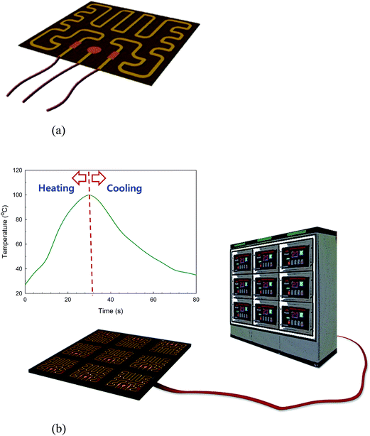
In the current study, we introduce a new mold wall control system, referred to as the local film heating system (LFHS) for securing the precise filling and cooling behaviors of molten polymer in the injection molding process. With the aid of such a system, the temperature of the mold surface can be controlled spatially and temporally, thus leading to uniform nanopatterns over the entire molded plastic surface. Among the required processing conditions of injection molding, the fast and active control of the mold wall temperature is one of the key factors for realizing the nanoinjection molding process.17–19 In a typical molding process, the mold surface is kept sufficiently hot during the filling step and is then cooled down to solidify the molten polymer using a water or oil flow based heat sink system. For heating the mold surface in the injection molding, various techniques have been proposed such as steam, induction, and laser. However, their inherent problems, such as low production rate and equipment expense, need to be resolved for practical application in the industry. In contrast, the LFHS enables rapid local heating and cooling of the mold surface, which can enhance the production rate (Fig. 1). To the best of our knowledge, this is the first pragmatic system that can not only control the distribution of the mold temperature in a systematic manner but also fabricate nanostructures with high precision and efficiency. We fabricated nanopatterned polymer structures while applying the LFHS system to the injection molding process and carried out numerical simulation for the molding process in order to understand the underlying physics behind the relevant material behaviors.
 |
| | Fig. 1 Illustration of local film heating system (LFHS): (a) a film heater that can heat and sense temperature simultaneously and (b) schematic image of the LFHS including a controller. The inset graph indicates the temperature variation of the LFHS as a function of time. | |
Experimental
Insert fabrication
For the photolithography, a Cr photomask with a size of 7 inch × 7 inch was made by using a mask generator (DWL 200, Heidelberg Instruments, Germany). A 〈100〉 Si wafer with a size of 6 inch was employed as a sacrificing layer, and Ti and Cr were vacuum-evaporated at thicknesses of 100 Å and 1000 Å, respectively for the metal seeding layer. Ti enhances the adhesive strength between the Cr and Si wafer, and Cr acts as a conductive seed layer, which is necessary for the subsequent Ni electroplating process.
Photoresist (PR) (THB 151N, JSR corp) was deposited at a thickness of 200 nm using a spin coating method. The thickness of the PR becomes the hole depth when the injection molded part is prepared. A negative photoresist was chosen to easily remove the photoresist after Ni electroplating was carried out after photolithography. In the spin coating process, two steps were applied at 300 rpm and 500 rpm because the viscosity of photoresist is high. After stabilizing the coating, the soft bake process was carried out at 120 °C for 40 min using a convection oven. Thereafter, a mask aligner (EVG640, Austria) was used to transfer the pattern from the fabricated mask to the PR coated wafer. The employed energy of UV light is 2200–2400 mJ cm−2. The nanostructure of the PR was materialized using a developer (DVL2000, JSR corp.).
The second metal seed layer, Cr was prepared using an E-beam evaporator, followed by the Ni electroplating on the PR structure. To remove the potential bubble between the nanostructures fabricated on the wafer, vacuum was applied before the Ni electroplating. The electroplating was conducted in 5 steps, increasing current intensity gradually, in an effort to minimize the residual stress of the Ni plate: (1) 100–500 mA for 60 min in the 1st step, (2) 600–1000 mA in the 2nd step, (3) 1100–2000 mA in the 3rd step, (4) 3500–4000 mA in the 4th step, and 7000 mA for 60 min in the 5th step. Finally, Ni was vacuum-evaporated with a thickness of 100–150 μm along the nanostructure materialized on the wafer. Subsequently, an Ni plate of about a 1000 μm thickness was developed using a relatively high current (approximately 1A level). Following the Ni electroplating, the Ni plate was cut into 10 cm × 10 cm using a wire cutting method for installation on the mold of an injection molding machine. In order to identify the nanostructured patterns, the surface of the Ni plate was observed using an atomic force microscope (AFM) (XE-100, PSIA, Korea) (Fig. 2).
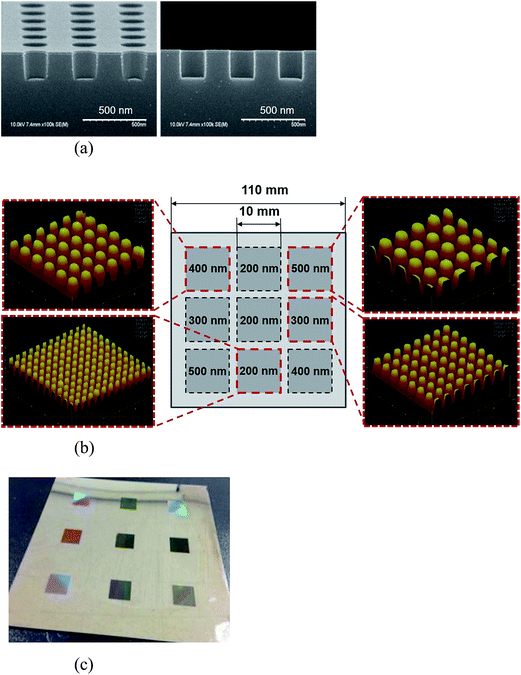 |
| | Fig. 2 (a) SEM image of nanoholes with a 200 nm diameter on the Si wafer, (b) schematic of nanopillar array and AFM images of the nanopatterned metal insert, and (c) Ni stamp with nanopatterns. | |
Injection molding
After the nanopatterned Ni stamp was polished, it was installed on the mold. For injection molding, cyclic olefin copolymer (COC) (TOPAS advanced polymers Co.) was employed. It consists of beads with a diameter of around 1 mm. Prior to injection molding, the resin was completely dried using a dehumidifier (Purpose VHM5-LC, HANSE cop) at 70 °C for 5 h in a vacuum environment. The temperature of the melting cylinder at the nozzle in the mold temperature itself and the temperature distribution on the mold surface were controlled using the cooling line of the mold and the LFHS introduced in this study. The mold was pre-warmed for 3 h to secure sufficient time for thermal equilibrium.
Injection molding analysis
We carried out numerical simulations for all the processes of injection molding in an attempt to understand LFHS embedded nanoinjection molding. The governing equations for filling the mold cavity are the continuity, the momentum, and the energy equations as follows:| |
 | (1) |
| |
 | (2) |
| |
 | (3) |
where ρ is the density, ṽ is the velocity vector, P is the pressure, ![[small tau, Greek, tilde]](https://www.rsc.org/images/entities/i_char_e0e5.gif) is the viscous stress tensor,
is the viscous stress tensor, ![[g with combining tilde]](https://www.rsc.org/images/entities/i_char_0067_0303.gif) is the gravity/body-force vector, Cp is the specific heat at constant pressure, β is the coefficient of thermal expansion, η is the so-called generalized Newtonian viscosity, and
is the gravity/body-force vector, Cp is the specific heat at constant pressure, β is the coefficient of thermal expansion, η is the so-called generalized Newtonian viscosity, and ![[q with combining tilde]](https://www.rsc.org/images/entities/i_char_0071_0303.gif) is the heat flux. Here,
is the heat flux. Here, ![[small gamma, Greek, dot above]](https://www.rsc.org/images/entities/i_char_e0a2.gif) is the shear rate,
is the shear rate,| |
 | (4) |
where (u, v) are the velocity components in the (x, y) directions. The flow front in the cavity is tracked using a fluid concentration equation, which can be expressed as| |
 | (5) |
where F is the fluid concentration. Since the polymer melt was regarded as a non-Newtonian viscous fluid in this study, the following modified Cross model was adopted for the fluid.| |
 | (6) |
where η is the viscosity, η0 is the zero shear rate viscosity, τ* is the shear stress at the transition between the Newtonian and the Power law behaviors and n is the Power law index. η0 can be represented as a function of temperature using the Williams–Landel–Ferry (WLF) equation:| |
 | (7) |
where T*(P) = D2 + D3P. The material constants for eqn (6) and (7) and COC are listed in Table 1 (Moldex3D).
Table 1 Material constants of the COC polymera
| n |
τ* (kPa) |
D1 (GPa) |
D2 (K) |
D3 (K Pa−1) |
A1 |
A2 |
| Here, n is the Power law index, τ* is the shear stress, and A1, A2, D1, D2 and D3 are empirical constants for fitting in eqn (7). |
| 0.428 |
36.632 |
9.46 × 10⁴ |
343.15 |
0 |
42.775 |
51.6 |
Optical analysis
The birefringence of an injection molded part was analyzed to examine the effect of fast and active control of the mold wall temperature in terms of the product quality. In general, the residual stress of molded parts causes the development of birefringence, especially in transparent plastics. The residual stress can be divided into two types: flow induced residual stress, which arises from molecular orientation in a cavity during filling, and thermally induced residual stress due to non-uniform cooling and shrinkage. In this sense, birefringence is affected by flow kinematics, temperature history, and temperature distribution during the processing stages such as the filling, packing, and cooling steps. Birefringence is defined as follows:where ne and no are the refractive indices experienced by the extraordinary and ordinary rays, respectively. The sign of birefringence can be either negative or positive, while the absolute value of the difference determines the total amount of birefringence. The birefringence value of a specimen is not fixed, but varies with the orientation of the crystal relative to the incident angle of illumination. The phase difference between the ordinary and extraordinary rays after they pass through a birefringent crystal is known as retardation:where δ is the retardation (as a length) and d is the thickness of the part through which rays pass. In the case where a polarized light passes through a birefringent material, fringes composed of light and shade appear. The magnitude, known as the fringe order N, is related to the differences among the principal stresses. The fringe order can be determined by the ratio of the retardation value to the wavelength of light, λ, as the following equation:| |
 | (10) |
For most materials, the indices of refraction remain constant. However, the index of polymers changes with respect to the applied stress. This can be described by the following stress-optic or Brewster's law:
| | |
n1 − n2 = CB(σ1 − σ2)
| (11) |
where
n1 and
n2 are the indices of refraction,
CB is the stress-optical coefficient, and
σ1 and
σ2 are the principal stresses.
Structural analysis
To achieve computational efficiency, the multi-scale method was introduced to solve thermal flow problems related with ejection of nanopillars in numerical simulation. It was a useful means describing the nanopillars within a nanopart as a decoupled solution.
In order to describe the large deformation phenomena of burr generation in an ejection stage, we carried out additional structural analysis by using the nonlinear hyperelastic model as a general Mooney–Rivlin material. The model used is a general Mooney–Rivlin hyperelastic material model defined by a polynomial. For such a material model, the strain energy density function has the following expression:
| |
 | (12) |
here
Ī1 and
Ī2 are the first and second invariant of the left isochoric Cauchy-Green deformation tensor,
Jel is the elastic Jacobian,
Ci,j are coefficients in the polynomial, and
K is the bulk modulus.
Results and discussion
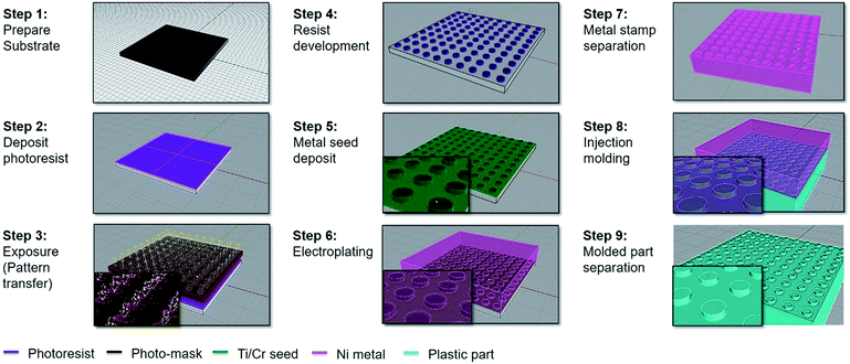
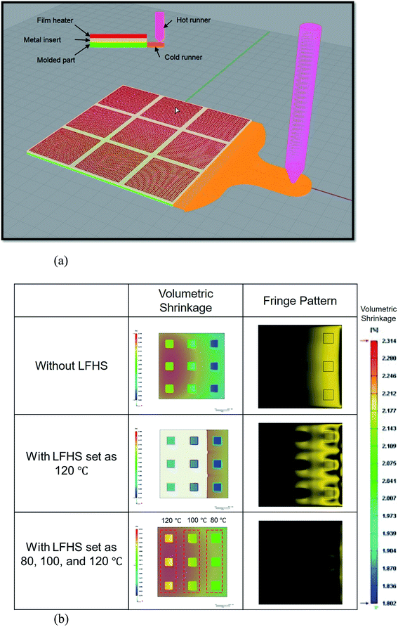
Cylindrical nanoholes with different dimensions were first designed and arrayed in a rectangular domain of 10 mm × 10 mm on the Si wafer (Fig. 2a), and the overall 9 domains were transferred and placed in the metal master of injection molding as shown in Fig. 2b and c. The cylindrical pillars were 200, 300, 400, and 500 nm in diameter and 200 nm in height. Fig. 3 presents a flow chart of all the processes used to fabricate the metal stamp and replicate nanopatterns using the master insert injection molding. It is important to note that for the nanoinjection molding process, a metal stamp with a complementary nanostructure needs to be prepared to replicate the designed nanopatterns. LFHS was applied to injection molding, and its effect was evaluated experimentally as well as numerically. We also found the optimal mold temperature distribution with the use of the LFHS. Fig. 4(a) presents the domains for injection molding simulation including the LFHS, cavity, mold insert, and runners. The inset of the figure demonstrates how the LFHS and the metal stamp were positioned in the mold. As can be seen in the figure, the LFHS and metal insert encompass 9 partitions, of which the temperatures can be controlled independently. As soon as a molten polymer is injected into the mold cavity through the hot runner and cold runner and comes into contact with the mold wall, the solidification of the polymer initiates. Once the LFHS keeps the mold wall sufficiently hot, the generation of the so-called skin layer in injection molded parts can be prevented. The contours of the volumetric shrinkage and optical fringe of the injection molded parts are presented in Fig. 4(b). Non-uniform volumetric shrinkage was observed in the overall molded part in the case without using the LFHS. The result of the optical fringe pattern was also similar to that of the non-uniform volumetric shrinkage. This is attributed to two reasons, low mold wall temperature and non-uniform mold wall temperature, even though the bulk mold temperature was controlled using a typical cooling line system. Considering this result, the mold wall temperature was then set to 120 °C as shown in Fig. 4(b). While LFHS was applied to the mold wall, the optical fringe pattern near the gate still somewhat differed to that at the end of the cavity due to the non-uniform volumetric shrinkage. For this reason, the 9 sections of the mold surface were grouped into three partitions according to the distance from the gate. In order to maximize the uniformity of the volumetric shrinkage over the entire molded part, the temperatures of the three partitions were set to 80 °C, 100 °C, and 120 °C with the use of LFHS. It was found that the volumetric shrinkage was uniform for all sections, thereby leading to a significantly reduced fringe pattern. This result indicates that if the mold wall temperature is locally controlled in the mold filling step, we can more actively adjust the inevitable generation of the skin layer on the mold wall and enhance the uniformity of the molded parts by modulating the thermally induced shrinkage and residual stress.20–22
 |
| | Fig. 3 Schematic diagram of the fabrication procedures for metal stamp using the MEMS techniques and for polymeric nanostructures using injection molding. | |
 |
| | Fig. 4 (a) Schematic description of the entire domain for injection molding simulation including the LFHS, cavity, mold insert, and runners and (b) volumetric shrinkage and fringe pattern of injection molded parts at different molding conditions. | |
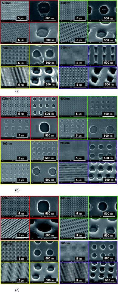
To identify the effect of LFHS on the replication quality of nanostructures, four different sized nanoholes of 200, 300, 400, and 500 nm were fabricated via injection molding. Fig. 5 shows SEM images of the nanopatterns. As expected, the case without using LFHS shows damaged patterns, especially for the 200 nm nanostructure. This can be explained by examining the result of the volumetric shrinkage. Namely, insufficient heating of the mold wall and non-uniform temperature distribution result in the poor replication quality of nanopatterns as shown in Fig. 5(a). When the entire mold wall temperature was modified to 120 °C with the LFHS, significantly enhanced nanopatterns were obtained, especially in the case of the 400 and 500 nm nanoholes. However, uniformly setting the mold wall temperature has a limitation for the fabrication of smaller nanopatterns such as 200 and 300 nm nanoholes (Fig. 5(b)). This problem could be solved by progressively increasing the mold wall temperature in the flow direction, which is expected to lead to a relatively uniform skin layer and cooling behavior of the polymer melt (Fig. 5(c)).
 |
| | Fig. 5 SEM images of injection molded nanostructures: (a) without LFHS, (b) with LFHS set to the uniform temperature of 120 °C, and (c) with LFHS set to local temperature distributions of 80, 100, and 120 °C. The images were taken for the center of the injection molded parts. | |
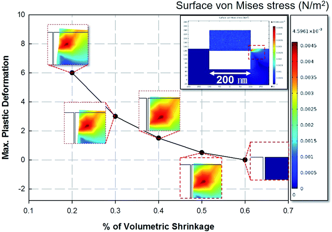
As explained above, the adjusted mold wall temperature can generate a uniform volumetric shrinkage over the entire molded part. This is one of key advantages of the LFHS. However, an unwanted defect of burrs appearing in the nanopatterns was observed in the SEM images. The generation of burrs is induced by the dissimilarity between the volumetric shrinkages of the polymer and the mold in the cooling and ejection steps of injection molding. The amount of volumetric shrinkage of polymers is strongly dependent on the cooling rate in the injection molding process.23–25 Subsequently, the shrinkage amount determines the burr generation phenomenon during ejection. To clarify this, we performed a structural analysis by using the Mooney–Rivlin material for the ejection process, considering the temperature history and material properties of the polymers and mold. Based on the stress–strain relation calculated, the nonlinear hyperelastic behavior of polymer was considered. As shown in Fig. 6, the plastic deformation of the plastics decreased with increasing the volumetric shrinkage. The inset shows the analysis domain adopted in the numerical simulation. Ejecting a molded part without generating burrs is critical for a successful injection molding process. Therefore, acquiring a proper amount of volumetric shrinkage is necessary for stable and robust ejection. When the volumetric shrinkage of polymers is not sufficient, burrs can be created on the edge of nanostructures due to the improper tolerance between the solidified polymer and the mold wall. The LFHS can allow tuning of the volumetric shrinkage of the polymer for ejecting the molded parts without damage. Overall, it is expected that the LFHS introduced in this study can provide a new route for manufacturing polymeric nanostructures by precisely controlling the local mold wall temperature.
 |
| | Fig. 6 Simulated plastic deformation as a function of the volumetric shrinkage in the ejection stage of injection molding. | |
Conclusions
In the study, we developed a new controlling system of the mold wall temperature and applied it to the injection molding process in order to fabricate polymeric nanostructures. Different sized nanoholes were prepared via injection molding by changing the condition of the mold wall temperature. To provide an in-depth physical understanding of the injection molding process using the LFHS, we carried out numerical simulations of the manufacturing process and optical and structural behaviors of the molded parts. Multiscale analysis was conducted combining macroscale and nanoscale simulations. The finding showed that the LFHS enabled the spatial and temporal control of the mold wall temperature in a systematic manner, which is a key requirement for implementing successful nanoinjection molding. In addition, the ejection behavior of the nanopatterns in the injection molding was modeled to offer insight into the optimal cooling and ejection conditions.
Acknowledgements
This research was supported by Basic Science Research Program through the National Research Foundation of Korea (NRF) funded by the Ministry of Education (2013R1A1A2059827). Also, this work was partially supported by the National Research Foundation of Korea (NRF) grant funded by the Korea government (MSIP) (2014R1A2A1A11053897). In addition, this research was supported by the Commercializations Promotion Agency for R&D Outcomes (COMPA) funded by the Ministry of Science, ICT and Future Planning (MISP). The authors are grateful for the support.
References
- S. Syrenova, C. Wadell and C. Langhammer, Nano Lett., 2014, 14, 2655–2663 CrossRef CAS PubMed.
- Y. Guo, S. R. Alvarado, J. D. Barclay and J. Vela, ACS Nano, 2013, 7, 3616–3626 CrossRef CAS PubMed.
- J. El-Ali, P. K. Sorger and K. F. Jensen, Nature, 2006, 442, 403–411 CrossRef CAS PubMed.
- A. Groisman, C. Lobo, H. J. Cho, J. K. Campbell, Y. S. Dufour, A. M. Stevens and A. Levchenko, Nat. Methods, 2005, 2, 685–689 CrossRef CAS PubMed.
- W. Sparreboom, A. van den Berg and J. C. T. Eijkel, Nat. Nanotechnol., 2009, 4, 713–720 CrossRef CAS PubMed.
- D. H. Lee, H. J. Oh, S. J. Bai and Y. S. Song, ACS Nano, 2014, 8, 6458–6465 CrossRef CAS PubMed.
- S. Jeong, C. Cho, H. Kang, K. H. Kim, Y. Yuk, J. Y. Park, B. J. Kim and J. Y. Lee, ACS Nano, 2015, 9, 2773–2782 CrossRef CAS PubMed.
- A. C. Siegel, S. S. Shevkoplyas, D. B. Weibel, D. A. Bruzewicz, A. W. Martinez and G. M. Whitesides, Angew. Chem., Int. Ed. Engl., 2006, 45, 6877–6882 CrossRef CAS PubMed.
- M. Kim, J. Kim and M. Allen, Small, 2015, 11, 1912–1918 CrossRef CAS PubMed.
- E. Leclerc, B. David, L. Griscom, B. Lepioufle, T. Fujii, P. Layrolle and C. Legallaisa, Biomaterials, 2006, 27, 586–595 CrossRef CAS PubMed.
- S. M. Kim, S. H. Lee and K. Y. Suh, Lab Chip, 2008, 8, 1015–1023 RSC.
- N. Szita, P. Boccazzi, Z. Y. Zhang, P. Boyle, A. J. Sinskey and K. F. Jensen, Lab Chip, 2005, 5, 819–826 RSC.
- X. Y. Hu, P. H. Bessette, J. R. Qian, C. D. Meinhart, P. S. Daugherty and H. T. Soh, Proc. Natl. Acad. Sci. U. S. A., 2005, 102, 15757–15761 CrossRef CAS PubMed.
- J. L. Tan, J. Tien, D. M. Pirone, D. S. Gray, K. Bhadriraju and C. S. Chen, Proc. Natl. Acad. Sci. U. S. A., 2003, 100, 1484–1489 CrossRef CAS PubMed.
- C. Jamora and E. Fuchs, Nat. Cell Biol., 2002, 4, E101–E108 CrossRef CAS PubMed.
- J. D. Martin, J. N. Marhefka, K. B. Migler and S. D. Hudson, Adv. Mater., 2011, 23, 426–432 CrossRef CAS PubMed.
- C. J. Bettinger, H. A. Becerril, D. H. Kim, B. L. Lee, S. Lee and Z. A. Bao, Adv. Mater., 2011, 23, 1257–1261 CrossRef CAS PubMed.
- Y. S. Song, D. Adler, F. Xu, E. Kayaalp, A. Nureddin, R. M. Anchan, R. L. Maas and U. Demirci, Proc. Natl. Acad. Sci. U. S. A., 2010, 107, 4596–4600 CrossRef CAS PubMed.
- D. B. Weibel and G. M. Whitesides, Curr. Opin. Chem. Biol., 2006, 10, 584–591 CrossRef CAS PubMed.
- J. C. Viana, A. M. Cunha and N. Billon, Polymer, 2002, 43, 4185–4196 CrossRef CAS.
- M. Fujiyama, T. Wakino and Y. Kawasaki, J. Appl. Polym. Sci., 1988, 35, 29–49 CrossRef CAS.
- J. C. Viana, N. M. Alves and J. F. Mano, Polym. Eng. Sci., 2004, 44, 2174–2184 CAS.
- D. Yao and B. Kim, Polym. Eng. Sci., 2002, 42, 2471–2481 CAS.
- H. Zuidema, G. W. M. Peters and H. E. H. Meijer, J. Appl. Polym. Sci., 2001, 82, 1170–1186 CrossRef CAS.
- R. Pantani, I. Coccorullo, V. Speranza and G. Titomanlio, Prog. Polym. Sci., 2005, 30, 1185–1222 CrossRef CAS.
|
| This journal is © The Royal Society of Chemistry 2015 |
Click here to see how this site uses Cookies. View our privacy policy here. 


![[small tau, Greek, tilde]](https://www.rsc.org/images/entities/i_char_e0e5.gif) is the viscous stress tensor,
is the viscous stress tensor, ![[g with combining tilde]](https://www.rsc.org/images/entities/i_char_0067_0303.gif) is the gravity/body-force vector, Cp is the specific heat at constant pressure, β is the coefficient of thermal expansion, η is the so-called generalized Newtonian viscosity, and
is the gravity/body-force vector, Cp is the specific heat at constant pressure, β is the coefficient of thermal expansion, η is the so-called generalized Newtonian viscosity, and ![[q with combining tilde]](https://www.rsc.org/images/entities/i_char_0071_0303.gif) is the heat flux. Here,
is the heat flux. Here, ![[small gamma, Greek, dot above]](https://www.rsc.org/images/entities/i_char_e0a2.gif) is the shear rate,
is the shear rate,


