Molecular orientation within thin films of isomorphic molecular semiconductors

Xiaofeng Liua, Mark A. Burgersa, Ben B. Y. Hsub, Jessica E. Coughlina, Louis A. Perezc, Alan J. Heegerb and Guillermo C. Bazan*acd
aCenter for Polymers & Organic Solids, Department of Chemistry and Biochemistry, University of California, Santa Barbara, CA 93106, USA. E-mail: bazan@chem.ucsb.edu
bDepartment of Physics, University of California, Santa Barbara, CA 93106, USA
cMaterials Department, University of California, Santa Barbara, CA 93106, USA
dKing Abdulaziz University, Jeddah 21413, Saudi Arabia

Received 22nd September 2015 , Accepted 12th October 2015

First published on 12th October 2015


Abstract

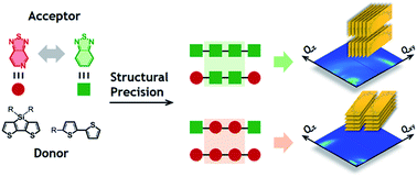
Four isomorphic organic semiconductors are compared to map out how the precision of chemical structures determines solid state molecular organization. Intramolecular electronic structure and intermolecular packing preference in the solid state were shown to be exclusively dependent on the relative location of the electron accepting fragments within a given molecule.


It is possible under certain processing conditions for conjugated molecules and polymers to approach the semiconducting properties of their inorganic counterparts.1–3 However, a significant challenge for practical implementation via solution processing arises from the absence of universal guidelines for managing the solid state organization as a function of molecular structure and deposition conditions.4–7 This lack of control prevents one to a priori preprogram design features in new molecules so to tailor the electronic coupling between molecules or polymer segments through control of their relative positions.8–11 The latter problem is particularly exacerbated if one would like optimal electronic coupling to occur along a particular charge transport direction, i.e., lateral or vertical, within a device configuration.

Organizing organic semiconductors from solution is difficult because one needs to manage weak intermolecular forces between the individual semiconducting subunits and solute/solvent interactions.12 The general aggregation and crystallization tendencies of molecular systems relate to the former and are dependent on structural parameters including the flexibility and size of solubilizing units, electrostatic distributions and molecular topology.13,14 Given that synthetic protocols are available for stitching together many already-developed aromatic subunits for creating a larger delocalized molecule,15–17 one often finds that the main challenge is not how to achieve a particular target, but rather how to down select from a vast matrix of possible structural variations.

What we have presented in this paper concerns a new class of molecular frameworks that has been successfully used in the fabrication of thin film transistors and solar cells.18–20 The general molecular structure can be expressed as D–A–D′–A′–D′′–A′–D′–A–D, where D corresponds to electron rich modules (donor) and A represents electron deficient units (acceptor). The current study provides a more detailed investigation on how these molecules self-assemble into useful bulk structures and inform the readers that achieving order does not require delicate control of thin film processing. They are also useful study subjects to understand to what extent one can isolate organizational and optoelectronic properties as a function of different molecular fragments.

We provide two new molecules (N0 and N2b) that were designed in view of the questions on self-assembly stated above. Specifically, we wish to probe how structural precision can be used to track the preference of molecular ordering in the bulk. Molecules in the study (N0, N2a, N2b, and N4, see Fig. 1a for chemical structures) were designed so to contain similar donor units, while altering the acceptor counterparts by interchanging between pyridyl[2,1,3]thiadiazole (PT) and benzo[c][1,2,5]thiadiazole (BT). The synthetic approach to molecules N0 and N2b can be found in the ESI. Chemical structures were confirmed by 1H/13C nuclear magnetic resonance spectroscopy and field desorption time-of-flight mass spectrometry. The sequence of structures in Fig. 1a allows us to compare differences in optical properties and solid-state arrangements between four nearly isomorphic organic semiconductors. As discussed in more detail below, “N” vs. “C–H” exchange within a relatively large molecule framework (molecular weight over 2200 Da) dominates molecular orientation, which emphasizes the importance of structural precision when a new material is designed.


image file: c5ra19606j-f1.tif
Fig. 1 (a) Chemical structures of molecules N0, N2a, N2b, and N4, with respective illustration highlighting their structural relationship. Green filled square represents BT and red filled circle represents PT (donor segments are omitted for clarity). (b) UV/vis absorption spectra of the corresponding four molecules in dilute chloroform solutions and in the solid state. (c) Dominant hole (left) and particle (right) natural transition orbitals for S0 → S1 transition of each molecule (from top to bottom: N0, N2a, N2b, and N4) in chloroform as calculated from TD-DFT under CAM-B3LYP/6-31G(d,p) basis set.

UV/vis absorption spectra (Fig. 1b) of N0, N2a, N2b, and N4 in dilute chloroform solution show molar absorption coefficients (ε) of the lowest energy peaks in the order of N2b < N0 < N4 < N2a, in which N2b shows the lowest ε (1 × 10⁵ M−1 cm−1) and the highest value (1.5 × 10⁵ M−1 cm−1) is observed for N2a. All molecules possess distinct charge-transfer absorption bands between 500 and 800 nm principally due to efficient D–A electronic communication.21 Given that donor elements are identical across these molecules, it is reasonable that the absorption edges should be dominated primarily by the electron affinity of the acceptor segments. Indeed, one observes that the bandgap (Eg) of N2a is narrower (1.41 eV) than for N0 (1.46 eV) because it contains a higher content of the more electron deficient PT fragments. However, molecules N2b and N4 have nearly identical absorption profiles, despite their structural differences: 2PT + 2BT (N2b) and 4PT (N4).

We employed time-dependent density functional theory (TD-DFT) to gain insight into the nature of the excited states.22–24 Fig. 1c illustrates the calculated dominant hole and particle natural transition orbitals (NTOs) for the S0 → S1 transition of each molecule based on the CAM-B3LYP/6-31G(d,p) basis set. As shown in Fig. 1c, the hole is well delocalized across the entire backbone in each molecular system. In contrast, comparison of the particle NTOs shows a more delocalized nature for N2a than for N2b, which qualitatively can be understood by the presence of the more electrophilic PT units at the termini of the N2a conjugated framework. This “stretching” of the particle orbital by the PT fragment is also observed when comparing N4 with N2b.

Table 1 summarizes the physical properties for molecules N0, N2a, N2b, and N4. The highest occupied molecular orbital (HOMO) energy levels of these molecules were estimated (in eV) as −4.95 (N0), −4.96 (N2a), −5.05 (N2b), and −5.19 (N4) from ultraviolet photoelectron spectroscopy (UPS) on layers obtained by solution-deposition of each molecule atop indium tin oxide. In combination with optical band gaps (1.46 eV, N0; 1.41 eV, N2a; and 1.36 eV, N2b and N4) obtained from the solid-state absorption edges (Fig. 1b), the lowest unoccupied molecular orbital (LUMO) energy levels were also estimated. This set of data indicates that HOMO and LUMO energy levels are determined not only by the relative numbers of PT/BT units, but also by how these acceptor fragments are arranged within the molecular framework. Thermal phase transitions of these materials were studied by differential scanning calorimetry (DSC). Melting (Tm) and crystallization (Tc) temperatures are detailed in Table 1. From the thermal transitions, one observes that all compounds have melting temperatures above 250 °C. The interplay between BT and PT does not seem to have obvious effect on the differences in Tm. However, at least within this series of compounds, the endmost PT units lead to a higher value of Tc (N2a/N4 vs. N0/N2b). Although a clear picture is not currently available to interpret thermal transitions relative to the chemical structures, as discussed in more detail below, a trend emerges that the combination of PT/BT functional groups plays a more significant role in directing the preferred molecular orientations in the solid state.

Table 1 Physical properties of molecules N0, N2a, N2b, and N4
Molecule Solution λmaxb (nm) Film λonsetc (nm) Egc (eV) EHOMOd (eV) ELUMOe (eV) Tm (°C) Tc (°C)
a Values obtained from ref. 18.b Obtained from dilute chloroform solutions with concentrations of 0.02 mg mL−1.c Thin films were prepared by spin-casting chloroform solutions (10 mg mL−1) of each molecule atop pre-cleaned glass slides with film thickness of 60–70 nm as determined by X-ray reflectivity measurement.d Estimated from UPS measurement with thin films (10–20 nm) atop ITO substrates.e Calculated by ELUMO = EHOMOEg.
N0 642 850 1.46 −4.95 −3.49 258, 269 238
N2aa 672 880 1.41 −4.96 −3.55 269 254, 244
N2b 712 915 1.36 −5.05 −3.69 259 221
N4a 715 915 1.36 −5.19 −3.83 265 246, 230


How molecular semiconductors orient themselves within thin films is relevant for understanding optoelectronic properties within a device configuration.25 Here, we present a detailed structural characterization on molecules N0, N2a, N2b, and N4 by using grazing incidence wide-angle X-ray scattering (GIWAXS) on spin coated thin films without subsequent thermal or solvent annealing treatments.26–29 Thin films were prepared by spin casting chloroform solution (10 mg mL−1) of each material atop silicon (100) substrates with resulting film thickness of 60–70 nm as determined from X-ray reflectivity measurement.19

Fig. 2a provides the 2D GIWAXS plots for thin films of N0, N2a, N2b, and N4. A summary of the relevant molecular features is depicted at the top-right corner of each image. Line cuts along both the out-of-plane (qz) and in-plane (qxy) directions are shown in Fig. 2b. All molecules exhibit distinct lamellar packing (denoted as (100)) and π–π stacking (010) diffractions. Interestingly, molecules N0 and N2a, both with two central BT units, show (100) peaks (q = 4.1 nm−1) preferentially oriented along the silicon substrate normal, with clear higher order peaks observed, i.e., (200) and (300). In contrast, molecules N2b and N4 exhibit (100) peaks (q = 3.6 nm−1) that are concentrated perpendicular to the silicon substrate normal. The lamellar d-spacings (d100) correspond to 1.5 and 1.7 nm for N0/N2a and N2b/N4, respectively, with similar crystallite coherence lengths (Lc) of 4–7 nm observed for all molecules. However, correlating these molecular organization features with their chemical structures points to how a delicate control of chemical structure (“C–H” vs. “N”) can lead to completely opposite crystallographic orientations across the majority of the film composition.


image file: c5ra19606j-f2.tif
Fig. 2 (a) 2D GIWAXS profiles for as-cast films of N0, N2a, N2b, and N4 atop silicon (100) substrates. Illustrations at the top right of each 2D image highlight the structural features of each molecule and provide possible visual correlations. (b) Out-of-plane and in-plane line-cuts obtained from the corresponding 2D GIWAXS profile. (c) Plots of scattering intensity as a function of azimuthal angle (χ) for both (100) and (010) peaks of each molecule.

In accordance to the preference of (100) peaks from this series of molecules, (010) peaks were observed also exclusively in an opposite orientation, going from N0/N2a to N2b/N4. The same d010 = 0.36 nm (q = 17.6 nm−1) was obtained regardless of the difference of crystallographic orientations. To illustrate more clearly the molecular orientations, pole figures (Fig. 2c) were extracted from each 2D GIWAXS plot (Fig. 2a) along both (100) and (010) diffractions.26,30,31 The polar angle, χ, is defined as the angle between the scattering vector and the silicon substrate normal. Since electronic coupling occurs more readily along the intermolecular π–π stacking direction rather than within lamellar alkyl chain interaction, the examination of pole figures for the (010) peaks are of particular relevance, where scattering peaks near χ = 0° and χ = ±90° are associated with molecular face-on and edge-on orientations, respectively. Defining R as the ratio between the integrated area where 0° < χ < 45° and the area where 45° < χ < 90°,32 one obtains R as ∼1[thin space (1/6-em)]:[thin space (1/6-em)]9 (10% vs. 90%), ∼1[thin space (1/6-em)]:[thin space (1/6-em)]9 (12% vs. 88%), ∼9[thin space (1/6-em)]:[thin space (1/6-em)]1 (89% vs. 11%), and ∼9[thin space (1/6-em)]:[thin space (1/6-em)]1 (92% vs. 8%) for N0, N2a, N2b, and N4, respectively. This set of data illustrates the degree to which the molecular orientation of N0/N2a is predominantly edge-on, while N2b/N4 exhibits primarily face-on with respect to the substrate surface. By looking at the molecular structures one thus determines that the preferential organization is dominated by the nature of the two interior acceptor groups.

In conclusion, we showcase four isomorphic organic semiconductors with the aim of mapping out how functional groups within a given molecule influence molecular aggregation in the solid state. It is generally acknowledged that the transition from solution to the solid state remains poorly understood both theoretically and experimentally.33–35 Simple guidance of how molecular semiconductors organize is not readily available and may ultimately prove to be system-dependent. However, within the class of donor–acceptor narrow band-gap organic semiconductors with intermediate dimensions discussed here, we are able to extract a relationship between the chemical structure and the preferred bulk molecular organization obtained via solution deposition. A “functional group”-dependent molecular organization emerges that the choice of the central electron-accepting groups correlates with molecular face-on/edge-on orientation. With increasing interest on this class of molecular semiconductors, these findings provide valuable insight to manage bridging single-molecule conformation with rather convoluted material bulk structure; a necessary step toward reliable electronic devices using molecular semiconductors.

Acknowledgements

The synthesis and characterization work was supported by the Department of the Navy, Office of Naval Awards No. N00014-14-1-0101. Part of the experiments were performed at the Advanced Light Source, Lawrence Berkeley National Laboratory, which is supported by the Director, Office of Science, Office of Basic Energy Sciences, of the U.S. Department of Energy under Contract No. DE-AC02-05CH11231. The MRL Shared Experimental Facilities are supported by the MRSEC Program of the NSF under Award No. DMR 1121053; a member of the NSF-funded Materials Research Facilities Network (http://www.mrfn.org). We acknowledge support from the Center for Scientific Computing from the CNSI, MRL: an NSF MRSEC (DMR-1121053) and NSF CNS-0960316. X. L. thanks Qin Yang for assistance in materials synthesis and Dr Michael A. Brady for help in GIWAXS data interpretation.

Notes and references

  1. H. J. Son, B. Carsten, I. H. Jung and L. Yu, Energy Environ. Sci., 2012, 5, 8158 Search PubMed.
  2. Y. Liu, J. Zhao, Z. Li, C. Mu, W. Ma, H. Hu, K. Jiang, H. Lin, H. Ade and H. Yan, Nat. Commun., 2014, 5, 5293 CrossRef CAS PubMed.
  3. Y. Yuan, G. Giri, A. L. Ayzner, A. P. Zoombelt, S. C. Mannsfeld, J. Chen, D. Nordlund, M. F. Toney, J. Huang and Z. Bao, Nat. Commun., 2014, 5, 3005 Search PubMed.
  4. J. R. Tumbleston, B. A. Collins, L. Yang, A. C. Stuart, E. Gann, W. Ma, W. You and H. Ade, Nat. Photonics, 2014, 8, 385 CrossRef CAS.
  5. N. E. Widjonarko, P. Schulz, P. A. Parilla, C. L. Perkins, P. F. Ndione, A. K. Sigdel, D. C. Olson, D. S. Ginley, A. Kahn, M. F. Toney and J. J. Berry, Adv. Energy Mater., 2014, 4, 1301879 CrossRef.
  6. D. Wang, F. Liu, N. Yagihashi, M. Nakaya, S. Ferdous, X. Liang, A. Muramatsu, K. Nakajima and T. P. Russell, Nano Lett., 2014, 14, 5727 CrossRef CAS PubMed.
  7. Y. Huang, X. Liu, C. Wang, J. T. Rogers, G. M. Su, M. L. Chabinyc, E. J. Kramer and G. C. Bazan, Adv. Energy Mater., 2014, 4, 1301886 CrossRef.
  8. S. Gélinas, A. Rao, A. Kumar, S. L. Smith, A. W. Chin, J. Clark, T. S. van der Poll, G. C. Bazan and R. H. Friend, Science, 2014, 343, 512 CrossRef PubMed.
  9. M. Oehzelt, N. Koch and G. Heimel, Nat. Commun., 2014, 5, 4174 CAS.
  10. K. R. Graham, C. Cabanetos, J. P. Jahnke, M. N. Idso, A. El Labban, G. O. Ngongang Ndjawa, T. Heumueller, K. Vandewal, A. Salleo, B. F. Chmelka, A. Amassian, P. M. Beaujuge and M. D. McGehee, J. Am. Chem. Soc., 2014, 136, 9608 CrossRef CAS PubMed.
  11. S. Foster, F. Deledalle, A. Mitani, T. Kimura, K.-B. Kim, T. Okachi, T. Kirchartz, J. Oguma, K. Miyake, J. R. Durrant, S. Doi and J. Nelson, Adv. Energy Mater., 2014, 4, 1400311 CrossRef.
  12. G. C. Bazan, J. Org. Chem., 2007, 72, 8615 CrossRef CAS PubMed.
  13. I. Osaka, M. Saito, T. Koganezawa and K. Takimiya, Adv. Mater., 2014, 26, 331 CrossRef CAS PubMed.
  14. G. C. Welch, R. C. Bakus II, S. J. Teat and G. C. Bazan, J. Am. Chem. Soc., 2013, 135, 2298 CrossRef CAS PubMed.
  15. E. Wang, W. Mammo and M. R. Andersson, Adv. Mater., 2014, 26, 1801 CrossRef CAS PubMed.
  16. J. Roncali, P. Leriche and P. Blanchard, Adv. Mater., 2014, 26, 3821 CrossRef CAS PubMed.
  17. J. Mei, Y. Diao, A. L. Appleton, L. Fang and Z. Bao, J. Am. Chem. Soc., 2013, 135, 6724 CrossRef CAS PubMed.
  18. X. Liu, Y. Sun, B. B. Hsu, A. Lorbach, L. Qi, A. J. Heeger and G. C. Bazan, J. Am. Chem. Soc., 2014, 136, 5697 CrossRef CAS PubMed.
  19. X. Liu, Y. Sun, L. A. Perez, W. Wen, M. F. Toney, A. J. Heeger and G. C. Bazan, J. Am. Chem. Soc., 2012, 134, 20609 CrossRef CAS PubMed.
  20. X. Liu, B. B. Hsu, Y. Sun, C. K. Mai, A. J. Heeger and G. C. Bazan, J. Am. Chem. Soc., 2014, 136, 16144 CrossRef CAS PubMed.
  21. Y. J. Cheng, S. H. Yang and C. S. Hsu, Chem. Rev., 2009, 109, 5868–5923 CrossRef CAS PubMed.
  22. R. L. Martin, J. Chem. Phys., 2003, 118, 4775 CrossRef CAS.
  23. S. Salman, J.-L. Brédas, S. R. Marder, V. Coropceanu and S. Barlow, Organometallics, 2013, 32, 6061 CrossRef CAS.
  24. A. Charaf-Eddin, B. le Guennic and D. Jacquemin, RSC Adv., 2014, 4, 49449 RSC.
  25. P. M. Beaujuge and J. M. Fréchet, J. Am. Chem. Soc., 2011, 133, 20009 CrossRef CAS PubMed.
  26. J. Rivnay, S. C. Mannsfeld, C. E. Miller, A. Salleo and M. F. Toney, Chem. Rev., 2012, 112, 5488 CrossRef CAS PubMed.
  27. R. Steyrleuthner, R. Di Pietro, B. A. Collins, F. Polzer, S. Himmelberger, M. Schubert, Z. Chen, S. Zhang, A. Salleo, H. Ade, A. Facchetti and D. Neher, J. Am. Chem. Soc., 2014, 136, 4245 CrossRef CAS PubMed.
  28. G. Giri, R. Li, D. M. Smilgies, E. Q. Li, Y. Diao, K. M. Lenn, M. Chiu, D. W. Lin, R. Allen, J. Reinspach, S. C. Mannsfeld, S. T. Thoroddsen, P. Clancy, Z. Bao and A. Amassian, Nat. Commun., 2014, 5, 3573 CAS.
  29. Y. Diao, B. C. Tee, G. Giri, J. Xu, H. Kim do, H. A. Becerril, R. M. Stoltenberg, T. H. Lee, G. Xue, S. C. Mannsfeld and Z. Bao, Nat. Mater., 2013, 12, 665 CrossRef CAS PubMed.
  30. J. L. Baker, L. H. Jimison, S. C. Mannsfeld, S. Volkman, S. Yin, V. Subramanian, A. Salleo, A. P. Alivisatos and M. F. Toney, Langmuir, 2010, 26, 9146 CrossRef CAS PubMed.
  31. L. J. Richter, D. M. DeLongchamp, F. A. Bokel, S. Engmann, K. W. Chou, A. Amassian, E. Schaible and A. Hexemer, Adv. Energy Mater., 2015, 5, 1400975 CrossRef.
  32. G. Kim, S. J. Kang, G. K. Dutta, Y. K. Han, T. J. Shin, Y. Y. Noh and C. J. Yang, J. Am. Chem. Soc., 2014, 136, 9477 CrossRef CAS PubMed.
  33. A. J. Pearson, T. Wang, A. D. F. Dunbar, H. Yi, D. C. Watters, D. M. Coles, P. A. Staniec, A. Iraqi, R. A. L. Jones and D. G. Lidzey, Adv. Funct. Mater., 2014, 24, 659 CrossRef CAS.
  34. F. Liu, Y. Gu, C. Wang, W. Zhao, D. Chen, A. L. Briseno and T. P. Russell, Adv. Mater., 2012, 24, 3947 CrossRef CAS PubMed.
  35. K. R. Graham, P. M. Wieruszewski, R. Stalder, M. J. Hartel, J. Mei, F. So and J. R. Reynolds, Adv. Funct. Mater., 2012, 22, 4801 CrossRef CAS.

Footnote

Electronic supplementary information (ESI) available: Detailed synthesis and characterization. See DOI: 10.1039/c5ra19606j

This journal is © The Royal Society of Chemistry 2015
Click here to see how this site uses Cookies. View our privacy policy here.