Mingdong Yia,
Jialin Guoa,
Wen Lia,
Linghai Xie*a,
Quli Fana and
Wei Huang*ab
aKey Laboratory for Organic Electronics and Information Displays & Institute of Advanced Materials (IAM), Jiangsu National Synergetic Innovation Center for Advanced Materials (SICAM), Nanjing University of Posts & Telecommunications, 9 Wenyuan Road, Nanjing 210023, China. E-mail: iamlhxie@njupt.edu.cn
bKey Laboratory of Flexible Electronics (KLOFE) & Institute of Advanced Materials (IAM), Jiangsu National Synergetic Innovation Center for Advanced Materials (SICAM), Nanjing Tech University (NanjingTech), 30 South Puzhu Road, Nanjing 211816, China. E-mail: iamwhuang@njtech.edu.cn
First published on 27th October 2015
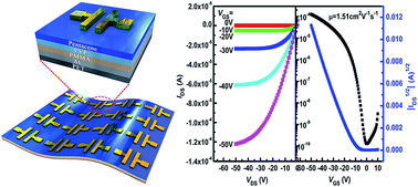
In this paper, we fabricated high performance flexible pentacene-based OFETs with low-k polymethylmethacrylate (PMMA, k = 3.5) and high-k dielectrics cross-linked poly(4-vinylphenol) (PVP, k = 4.1) as double gate insulator layers on poly(ethylene terephthalate) (PET) plastic substrate. The field-effect mobility (μ) of flexible pentacene-based OFETs was greatly increased from 0.66 cm2 V−1 s−1 to 1.51 cm2 V−1 s−1, meanwhile, their high electrical insulating properties were also well maintained which resulted in high ON/OFF current ratio of 105. The control experiments showed that the high performance flexible OFETs were mainly attributed to the PMMA/PVP double dielectric layers which not only have high electrical insulating property but also favor the growth of pentacene films. The flexible OFETs still showed excellent mechanical flexibility when they were bent 1000 successive mechanical bending cycles and held under the bending state for 2 hours at a radius of 3.5 mm. In addition, the flexible OFETs also showed high thermal stability, which exhibited the mobility of 0.72 cm2 V−1 s−1, the positive shift direction of VTH, the ON/OFF current ratio of 105 after heating to 100 °C for 2 hours in the atmosphere. Our results suggested that the PMMA/PVP double dielectric films were very suitable for the dielectric layer of the flexible OFETs.
In this study, we used polymer dielectrics high-k PVP and low-k PMMA as double gate insulator layers of flexible pentacene-based OFETs on PET substrate by low-temperature solution processing. The PMMA/PVP double dielectric layers effectively improved both the field-effect mobility and the electrical insulating properties of flexible pentacene-based OFETs. The causes of the advantage of PMMA/PVP double dielectric layers were studied by control experiments. In addition, we further measured the mechanical flexibility and thermal stability of flexible pentacene-based OFETs with PMMA/PVP double dielectric layers, and the results were characterized by atomic force microscope (AFM) and the X-ray diffraction (XRD).
000) solution was spin-coated on the Al substrate to form the first gated insulator layer with a thickness of about 400 nm. Subsequently, a 20 mg mL−1 cross-linked PVP (Mw ∼ 11
000) solution was spin-coated on the PMMA film to the second gate insulator layer with a thickness of about 80 nm. Then, the substrate was transferred to the oven to be cross-linked for 2 hours at 100 °C in air. After that, a 50 nm thick pentacene film as the semiconductor layer was thermally evaporated onto the double polymer gate insulator (PMMA/PVP) layers at a deposition rate of 0.1 Å s−1 at a pressure of 5 × 10⁻⁴ Pa. Finally, a 50 nm thick gold (Au) film was also thermally evaporated through shadow masks to form source and drain electrodes with the channel width (W = 2000 μm) and the channel length (L = 100 μm), respectively. The electrical properties of flexible pentacene-based OFETs with PMMA/PVP double dielectric layers were measured by an Agilent B1500A semiconductor parameter analyzer, and the thickness of Al, PMMA, cross-linked PVP, pentacene and Au film were measured by Bruker Dektak XT stylus profiler. All electrical measurements were carried out under ambient conditions.
In order to clarify the advantage of PMMA/PVP dielectric films as double gate insulator layers in OFETs, we measured the leakage current of PET/Al/dielectric films (PVP (480 nm), PVP/PMMA (480 nm), PMMA/PVP (480 nm) and PMMA (480 nm))/pentacene/Au, as shown in Fig. 2a. It can be found that the current density (J) of the other three dielectric films except PVP film can be kept in the range of 10−10 A cm−2 and 10−9 A cm−2 even if the applied voltage arrived at ±10 V, showing that the electrical insulating properties of three dielectric films (PMMA, PVP/PMMA and PMMA/PVP) were very good. However, the J jumped abruptly from the low conductance to the high conductance as the applied voltage further increased. From the value of the jumped voltage, we can inferred that the electrical insulating property of the PMMA film was the highest, followed by the PVP/PMMA film, PMMA/PVP film, and PVP film. The electrical insulating properties of four dielectric films with four different dielectric films showed that PMMA film can effectively improve the electrical insulation ability of the dielectric layer. The quality of organic semiconductor growth is very important for the OFETs, so the atomic force microscope (AFM) images of 10 nm pentacene films grown on dielectric films (PVP, PVP/PMMA, PMMA/PVP and PMMA)/Al/PET substrate were characterized, as shown in Fig. 2b. It can be seen that the pentacene films grown on both PMMA/PVP and PVP films were composed of the grains with distinct terraces, which showed the pentacene films of higher crystallinity.33 In contrast, the terraces of pentacene grains which composed of pentacene films on both PVP/PMMA and PMMA films were very vague, suggesting that the crystallinity of pentacene films decreased. The AFM results demonstrated that the pentacene film on the PVP film can grow better than that of on the PMMA film, which can effectively enhance the μ of the OFETs, as shown in Fig. 1c. It should be noted that the terraces of pentacene grains on PMMA/PVP films was clearer than that of on PVP films, showing that the growth of pentacene films on PMMA/PVP films was more favourable than PVP films which revealed the cause of high μ of flexible pentacene-based OFETs with PMMA/PVP double dielectric layers. In addition, the PMMA/PVP dielectric films could be prepared by low-temperature solution processing, which is well compatible with plastic substrate to endure the successive mechanical bending. Therefore, the PMMA/PVP dielectric films are very suitable for the gate insulator layer of the flexible OFETs due to their high electrical insulating properties, improving the organic semiconductor film growth and natural flexibility.
Fig. 3 showed the mechanical bending stability of the flexible OFETs with PMMA/PVP double dielectric layers. The transfer characteristics of the flexible OFETs as a function of the mechanical bending cycles with the bending direction aligned parallel and vertical to the channel direction when the bending radius was fixed at 3.5 mm, as shown in Fig. 3a. It can be seen that the shift of the transfer curves was not apparent after 1000 mechanical bending cycles with the bending direction aligned parallel as well as vertical to the channel direction, and the variation in VTH with the two bending directions was only within 2 V, as shown in Fig. 3b, indicating that the charge traps induced by the mechanical bending was very little in the PMMA/PVP double dielectric layers.5,34,35 Although μ of our flexible decreased as the mechanical bending cycles increased, it still remained to be 0.3 cm2 V−1 s−1 after 1000 mechanical bending cycles, as shown in Fig. 3b. Fig. 3c showed the variation in the ON and OFF current of the flexible OFETs. During the successive mechanical bending cycles, the variation in both ON and OFF current showed a slight reduction, and the stable ON/OFF current ratio of 104 was achieved which is high enough to control the AMOLEDs and logic circuits. It should be noted the OFF current always was kept in the range of 10−9 A and 10−12 A under both parallel and vertical bending direction conditions, showing that the successive mechanical bending did not significantly affect the electrical insulating properties of the PMMA/PVP double dielectric layers. So we can infer that the reduction of the on current was attributed on the conductivity degradation of pentacene films rather than PMMA/PVP dielectric layers.5 We also measured the electrical characteristics of the flexible OFETs under the bending states. Fig. 3d showed the transfer characteristics of the flexible OFETs as function of the mechanical bending time with the bending direction aligned parallel and vertical to the channel direction. The shift of the transfer curves under two bending states was very smaller even if the bending time was approximately 2 hours at a radius of 3.5 mm, correspondingly the variation in VTH under two bending states was less than 1.5 V, as shown in Fig. 3e. The variation in both ON and OFF current remained relatively stable, and the ON/OFF current ratio of 105 and 104 could be obtained during the different bending time, as shown in Fig. 3f. In addition, the OFF current of the other five flexible OFETs with PMMA/PVP double dielectric layers were measured as a function of the mechanical bending cycles and mechanical bending time, as shown in ESI Fig. S2.† Their OFF current also showed no noticeable degradation, further showing that the PMMA/PVP dielectric layers could sustain the long-term bending strain without larger leakage current. However, as the bending time increased, the μ correspondingly decreased from 1.63 cm2 V−1 s−1 to 0.73 cm2 V−1 s−1 and from 1.52 cm2 V−1 s−1 to 0.20 cm2 V−1 s−1 for the parallel and perpendicular bending direction, respectively. The stable variation of the OFF current indicated that the decrease of μ was also mainly attributed to the reduction in electrical conductivity of pentacene film rather than PMMA/PVP dielectric layers, which was further confirmed by reduction in electrical conductivity of the diodes with structure of Au/pentacene/Au of flexible OFETs with the creasing of the mechanical bending cycles and mechanical bending, as shown in ESI Fig. S3.† The above bending properties of the flexible OTFTs demonstrated that the PMMA/PVP dielectric films had excellent mechanical flexibility and high electrical insulating properties, which could be promising candidates for the high performance flexible OFETs.
We measured the thermal stability of the flexible OFETs with PMMA/PVP double dielectric layers. Fig. 4a showed the transfer curves as a function of the heating temperatures which was varied from 20 °C to 140 °C in steps of 20 °C, and each heating temperature was kept for 2 hours. The shift of the transfer curves was very little when the heating temperature increased from 20 °C to 100 °C. The noticeable variation in the negative shift of the transfer curves was observed until the heating temperature exceeded 100 °C. The μ and VTH of the flexible OFETs as function of heating temperature were shown in Fig. 4b. Although the μ decreased as the heating temperature increased, it still maintained 0.72 cm2 V−1 s−1 after heating the samples at 100 °C for 2 hours which was higher than the pentacene-based OFETs on the rigid substrate at room temperature. Interestingly, as the heating temperature increased, the threshold voltage gradually shifted toward the positive direction rather than negative direction, which was opposite to that presented in the previous report.31,36,37 The positive shift direction of VTH in our flexible OFETs indicated that the charge traps in the interface between PMMA/PVP film and pentacene film could be reduced as the heating temperature increased.28,30,31,36 The variation in the ON and OFF current of the flexible OFETs as function of heating temperature were shown in Fig. 4c. When the heating temperature increased from 20 °C to 140 °C, the variation in ON current decreased from 1.30 × 10⁻⁴ A to 4.63 × 10⁻⁶ A, which can mainly be ascribed to the reduction in electrical conductivity of pentacene film.38,39 On the other hand, the OFF current also decreased during the heating process, but it was still located between 10−9 A and 10−10 A even if the heating temperature increased to 140 °C, showing that the high heating temperature had little impact on the electrical insulating properties of the PMMA/PVP dielectric layers. In addition, the flexible OFETs showed an increase in the ON/OFF current ratio when the heating temperature was varied from 40 °C to 100 °C, and the 105 can be maintained during the above heating process, as the heating temperature further increased from 100 °C to 140 °C, the ON/OFF current ratio decreased from 105 to 103. Eventually, a high ON/OFF current of 105 and 104 could be achieved in our flexible OFETs under higher heating temperature. It can be seen that the drastic change in the electrical parameters of the flexible OFETs can be observed after the heating temperature exceeded 100 °C, and the temperature is near to the phase transition temperature of pentacene crystal,29–31 so it is reasonable to assume that the drastic change in electrical parameters of our flexible OFETs was related to the phase transition of pentacene films which caused by the high heating temperature. The study of thermal stability showed that the flexible OFETs with PMMA/PVP double dielectric layers could still operate well under the high temperature without any encapsulation layers.
In order to gain more insight on thermal stability of the flexible OFETs with PMMA/PVP double dielectric layers, the AFM and the X-ray diffraction (XRD) characteristics of pentacene films and PMMA/PVP films at four typical heating temperatures (20 °C, 60 °C, 100 °C and 140 °C) were investigated, as shown in Fig. 5. Fig. 5a showed the AFM images of PMMA/PVP films on Al/PET substrate at four typical heating temperatures. It was found that there was no obvious distinction in the surface morphologies of the four samples, indicating that the thermal stability of PMMA/PVP films were considerably more stable. The AFM results of the PMMA/PVP films were consistent with the change in OFF current of the flexible OFETs at different heating temperatures. Fig. 5b showed AFM images of 10 nm thick pentacene films grown on PMMA/PVP/SiO2/Si substrate at four typical heating temperatures (20 °C, 60 °C, 100 °C and 140 °C). It can be seen that the terraces of pentacene grains which composed of pentacene films gradually vague as the heating temperature increased, suggesting that the crystallinity of pentacene films decreased with the increasing of the heating temperature which caused the decrease of the field-effect mobility.40 The AFM films of the pentacene films at four heating temperatures were consistent with the change in field-effect mobility of the flexible OFETs at different heating temperatures. The XRD of 50 nm thick pentacene films grown on PVP/PMMA/SiO2/Si substrate also supported the AFM results of pentacene films at different heating temperatures, as shown in Fig. 5c. As the heating temperature increased from 20 °C to 140 °C, the (001) peak intensities of pentacene films gradually decreased, which were consistent with the variation in the terrace's clarity of pentacene grains at the different heating temperature, as shown in Fig. 5b. In addition, when the heating temperature exceeded 100 °C, the (001) peak intensities of pentacene films drastically reduced, showing that phase change of pentacene films was most likely to happen in the case, which resulted in the drastic change in the electrical parameters of the flexible OFETs. The above AFM and XRD results further confirmed that the decrease of the field-effect mobility with increased temperature were mainly caused by the reduction in electrical conductivity of pentacene film rather than PMMA/PVP dielectric layers.
Footnote |
| † Electronic supplementary information (ESI) available. See DOI: 10.1039/c5ra18996a |
| This journal is © The Royal Society of Chemistry 2015 |