Chemical and mechanical strains tuned dielectric properties in Zr-doped CaCu3Ti4O12 highly epitaxial thin films

M. Gaoa, D. Fenga, G. Yaoa, Y. Zhanga, C.-L. Chenbc and Y. Lin*ad
aState Key Laboratory of Electronic Thin Films and Integrated Devices, University of Electronic Science and Technology of China, Chengdu, Sichuan 610054, P. R. China. E-mail: linyuan@uestc.edu.cn
bDepartment of Physics and Astronomy, University of Texas at San Antonio, San Antonio, Texas 78249, USA
cDepartment of Physics and The Texas Center for Superconductivity, University of Houston, Houston, Texas 77204, USA
dInstitute of Electronic and Information Engineering in Dongguan, University of Electronic Science and Technology of China, Dongguan, Guangdong 523808, P. R. China

Received 6th September 2015 , Accepted 26th October 2015

First published on 26th October 2015


Abstract

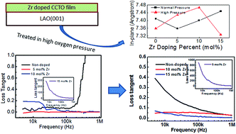
The nature of strain tuned dielectric properties in CaCu3Ti4O12 (CCTO) films was systematically studied with chemical strain (various doping rates) and physical strain (different oxygen pressure treatments). Microstructural characterization revealed that the lattice parameters of the highly epitaxial CCTO thin films are strongly dependent upon both Zr doping rates and annealing oxygen pressures. Dielectric property measurements indicate that the dielectric loss can be tuned by optimizing the doping rate and annealing oxygen pressure. These findings indicate that the dielectric properties of CCTO can be manipulated by the in-plane strain achieved from either chemical or physical treatment.


Introduction

With the rapid development of modern microelectronic technology and the demands of energy systems, integrated electronic circuits require dielectric materials with high dielectric constants and low dielectric loss to enhance device functionalities and reduce device dimensions.1,2 CaCu3Ti4O12 (CCTO), a perovskite-related material with its unusual high dielectric constant, has attracted great attention in the last decades due to its high dielectric constant in a broad temperature range and a wide frequency region.3–5 However, the relatively high dielectric loss of CCTO has significantly restrained its practical applications in device development.6,7 Various techniques have been applied to enhance its dielectric properties. Among them, the doping technique has been considered as a practical method to tune the dielectric behavior of CCTO.8–13 Although the doping of Mn, Nb or Fe in CCTO has showed an obvious reduction in the dielectric loss of CCTO ceramics, the dielectric permittivity was dramatically decreased by about three orders of magnitude.9,12 It has been reported that ZrO2 in CCTO ceramics can not only lower the dielectric loss but also maintain its high dielectric permittivity over a wide range of temperature and frequency.8 It was considered to be related to the presence of ZrO2 at the grain boundaries, which can reduce the grain boundary conductivity so as to decrease the dielectric loss of CCTO ceramics.8,14 However, this research was focused on bulk ceramics with small doping ratios.

To understand the nature of doping effects on the physical properties of CCTO for practical device development, it is critical to systematically study the dielectric properties of the doped CCTO with single crystallinity. Unfortunately, there is no single crystal CCTO with various doping available. Therefore, epitaxial CCTO films with various doping ratios become a practical technique to tackle these fundamental issues. On the other hand, the interfacial strain in the epitaxial thin films, crucial to the performance of thin-film devices,15 may couple with the chemical strain induced from doping ratio to tune the dielectric properties. Our previous study revealed that a proper high oxygen pressure annealing can significantly reduce the dielectric loss of CCTO film since a high oxygen pressure annealing can decrease the oxygen vacancy density in the CCTO films.16 Therefore, it is practical to combine both chemically Zr doped treatments and physically high oxygen pressure annealing to optimize the dielectric properties of the epitaxial CCTO thin films and to further establish the relationship of dielectric properties, microstructures, and chemicals of CCTO films.

Recently, we have investigated the evolvements of the microstructures and the dielectric properties in CCTO epitaxial films with chemical treatments by various doping rates of Zr and physical annealing under various oxygen pressures (from 0.1 to 0.55 MPa). It is surprisingly found that by optimizing the epitaxial quality, the lattice parameters and the physical properties of the CCTO films can be significantly affected by the chemical and physical treatments or specifically, the dielectric permittivity is determined by the in-plane stain which can be tuned by either physical or chemical modifications.

Experimetal details

A polymer-assisted deposition (PAD) technique17 was adopted to fabricate Zr-doped CCTO films on LaAlO3 (001) substrates with various doping ratios. The metal polymeric liquid precursors were prepared by Ca(NO3)2, Cu(NO3)2, Ti(cat)3(NH4)2 and polyethylenimine, as seen in the previous report.16 The concentrations of metal ions in the solutions were measured by inductively coupled plasma-atomic emission spectrometer (ICP-AES). Thus, the solutions with molar ratio of Ca[thin space (1/6-em)]:[thin space (1/6-em)]Cu[thin space (1/6-em)]:[thin space (1/6-em)]Ti = 1[thin space (1/6-em)]:[thin space (1/6-em)]3[thin space (1/6-em)]:[thin space (1/6-em)]4 were mixed together to yield the final precursor solution for CCTO. Then, Zr4+ solution was mixed with the CaCu3Ti4 precursor solution to achieve the deposition solution with various molar ratios of Zr4+/Ca2+, i.e., 5 mol%, 10 mol% and 15 mol%. The as-prepared solutions were spin-coated on the LaAlO3 (001) substrates to form the precursor films. The precursor films were gradually heated from room temperature to 510 °C to burn out the polymer. The films were then heated from 510 to 900 °C slowly in pure oxygen atmosphere under a normal oxygen pressure (0.1 MPa) or a high oxygen pressure (0.55 MPa) using a high pressure tube furnace (MTI OTF 1200x), and kept at 900 °C for 10 hours under the same oxygen pressure condition before being naturally cooled down to room temperature. The thicknesses of CCTO films are about 150 nm, which were determined by scanning electron microscopy. X-ray diffraction (XRD) was employed to characterize the lattice structures and phases of the as-prepared CCTO films. The interdigital capacitance measuring technique was applied to determine the dielectric properties of the as-grown Zr-doped CCTO films.18,19 Au/Ni electrodes with cross-finger-shape were prepared on the surface of the CCTO thin films by DC-sputtering technique. The interdigital pattern has a total of 100 fingers with a finger length of 400 μm, a finger width of 20 μm, and a finger gap of 20 μm. Capacitance and loss tangent of the films were measured by an Agilent 4294A Precision Impedance Analyzer.

Results and discussion

Similar to our previous results, the CCTO films can be epitaxially grown on LAO (001) substrates.16 Fig. 1 shows the normal (χ = 0°) and tilted (χ = 45°) θ–2θ XRD scanning patterns for the CCTO doped films with different Zr proportions (chemically treated) under different oxygen pressure treatments (physically treated). The chemically treated films under normal pressure treatment (0.1 MPa) reveals that the (004) peak of CCTO shifts to lower angles with the increase of the Zr proportion, as seen in Fig. 1(a). Surprisingly, both the chemically and physically treated films under high oxygen pressure (0.55 MPa) show that the (004) peaks of CCTO films shift to higher angles when the doping rates are higher than 10 mol%, as shown in Fig. 1(b). In addition, the tilted (χ = 45°) θ–2θ XRD scanning patterns indicate that the (202) peak of chemically treated CCTO films shifts to a higher angle for the 5 mol% Zr-doped sample and then shifts back to a lower angle with the increase of the Zr proportion, while the (202) peak of both chemically and physically treated CCTO films shifts to a lower angle with the increase of the Zr proportion except for the 15 mol% Zr-doped film treated under high oxygen pressure, as shown in Fig. 1(c) and (d). The in-plane (a- and b-axis) and out-of-plane (along c-axis) lattice parameters of CCTO films can be derived from the normal and tilted θ–2θ XRD scanning spectra, as seen in Fig. 2. The out-of-plane lattice parameters of the chemically treated CCTO films, under normal pressure, linearly increase with the increase of the Zr proportion. This is reasonable since the ionic radius of Zr4+ (0.72 Å) is larger than that of Ti4+ (0.53 Å). Therefore, the more substitution of Ti4+ by Zr4+, the larger the lattice parameters of the Zr-doped CCTO films. However, the out-of-plane lattice parameter for both the chemically and physically treated CCTO films under high oxygen pressure shows a zig-zag changing trend. The mechanisms resulting in these phenomena are not fully understood yet. Since the out-of-plane lattice does not bare the regulation from the substrate, the evolution is most likely resulted from the passion ratio and the in-plane strains, as well as the chemical stress from doping. To clearly demonstrate the change of the strains in the doped-CCTO films, the out-of-plane and in-plane strains of the as-prepared films were calculated based on the lattice parameters of bulk CCTO (7.393 Å) and listed in Table 1.
image file: c5ra18149f-f1.tif
Fig. 1 Normal (χ = 0°) and tilted (χ = 45°) XRD θ–2θ scanning patterns of CCTO films doped with different proportions of Zr and annealed under different oxygen pressure: 0.1 MPa (a and c) and 0.55 MPa (b and d), respectively.

image file: c5ra18149f-f2.tif
Fig. 2 The out-of-plane (a) and in-plane (b) lattice parameters of doped-CCTO films versus the proportions of Zr for samples annealed under normal oxygen pressure (0.1 MPa) and high oxygen pressure (0.55 MPa). (c) The calculated unit cell volumes of doped-CCTO films with the proportions of Zr.
Table 1 The calculated out-of-plane and in-plane strains of doped-CCTO films annealed under normal oxygen pressure (0.1 MPa) and high oxygen pressure (0.55 MPa)
Zr doping percentage (mol%) Out-of-plane (%) In-plane (%)
Normal pressure High pressure Normal pressure High pressure
0 −0.11 0.31 0.22 −0.46
5 −0.03 0.44 −0.48 0.50
10 0.09 0.35 0.10 1.00
15 0.20 0.45 0.75 −0.89


As shown in Fig. 2(b), the in-plane lattice parameters of the chemically treated films also basically increase with the increase of the Zr proportions. It should be pointed out that the in-plane lattice parameters are reduced from 7.41 Å for un-doped CCTO film to 7.36 Å for 5 mol% Zr-doped film for the normal pressure annealed samples. The in-plane lattice parameters for the physically treated films (the high pressure annealed samples) gradually increase with the doping proportions from 7.40 Å to 7.46 Å nm for the 10 mol% Zr-doped film before its sudden drop to 7.33 Å for the 15% Zr-doped films. This may result from the residual in-plane tensile strain effects due to the different thermal expansive coefficients for LAO and CCTO systems. Since the lattice parameter of the LAO substrate (3.79 Å) is larger than half of the lattice parameter of the bulk CCTO (∼3.7 Å), the in-plane tensile strain would be induced in the CCTO films during the epitaxial growth. On the other hand, since the thermal expansion coefficient for LAO [∼10 × 10−6/°C] is slightly larger than CCTO [4.4 × 10⁻⁶/°C],7,20 the interface compressive strain will accumulate during the cooling process from 900 °C to room temperature. The residual interface strains are therefore dependent upon the competition of the lattice and thermal misfits between the LAO substrate and the CCTO film systems. For the CCTO films doped with a small amount of Zr, i.e. 5 mol%, the doping induced chemical strain may help release the strain induced by lattice misfit at the crystallization temperature. In this case, the compressive strain induced by thermal misfit during the cooling process would gradually dominate the final in-plane strain in the film with more Zr dopants. In other words, the in-plane lattice parameters decrease with the increase of the doping rates from 0 to 5 mol% for the normal pressure annealed samples. Then, with further increases of the doping rates, since there will be more the substitution of Ti4+ by Zr4+, leading to larger lattice parameters, the chemical tensile strain will start to dominate the lattice structure and make the in-plane lattice parameter of the film increase. For both chemically and physically treated CCTO films (high pressure annealed doped-samples), as shown in Table 1, the tensile interfacial strain and chemical strain gradually dominate the in-plane lattice parameter when the Zr doping rate increases from 1 to 10 mol%. But when the tensile strain is beyond the capability of the CCTO lattice (doped with 15% Zr), the in-plane lattice parameter drops to its smallest value. Also, the volume of one unit cell can be calculated from the as-achieved lattice parameters, as shown in Fig. 2(c). The trend of the unit cell volume with the proportion of Zr is similar to that of the in-plane lattice parameters.

The dielectric properties of the as-prepared CCTO thin films were characterized from 5 kHz to 1 MHz. Fig. 3 is the dielectric properties of the Zr doped CCTO films annealed under the normal pressure (chemically treated). It is found that small amount of Zr doping (5 mol%) can significantly decrease the dielectric loss of the film by an order of magnitude compared to non-doped film although it only slightly decreases its dielectric constant. While the doping amount is increased to 10 mol%, the dielectric constant of the film reaches to about 600, or about 1/3 higher than that from the non-doped sample, and the dielectric loss is still smaller than that from the non-doped sample when the frequency is higher than 30 kHz. However, the further increase of the Zr doping amount to 15 mol% results in the dramatic increase of the dielectric loss, about three orders of magnitude higher than that from the non-doped films. By carefully evaluating the lattice parameters shown in Fig. 2, it is obvious that the huge increase of the dielectric loss is highly related to the in-plane lattice parameters. In other words, the smaller the in-plane lattice parameters, the less the dielectric loss. It should be also noted that a large fluctuation of dielectric constant with the frequency was observed for samples with high doping rates (10% and 15%), which may be related to the inhomogeneity of the films induced by the large amount of Zr doping.


image file: c5ra18149f-f3.tif
Fig. 3 The dielectric properties for different proportions of Zr doped-CCTO films annealed under normal oxygen pressure (0.1 MPa): (a) the dielectric constants of thin film samples, (b) the dielectric loss of thin film samples.

Fig. 4 shows the dielectric behavior for the as-grown films, both chemically and physically treated under high oxygen pressures. Although the Zr doping does not significantly change the dielectric constants of the samples, it can stabilize the dielectric spectra in the measured frequency ranges, which may possibly be attributed to the improved homogeneity of the doped-samples by the high pressure treatment. Especially, as seen in Fig. 4(b), the dielectric loss reaches its smallest value in the 15 mol% Zr doped film. More exactly, the 15 mol% Zr-doped CCTO shows the lowest dielectric loss values with the most steady dielectric constant spectra in the as-measured frequency range. Clearly, the lowest dielectric loss is also achieved in the Zr-doped film with the smallest in-plane lattice. This physically treated result is in good agreement with the conclusions from the chemically treated results under the normal pressure treatments. However, it should be noted that as shown in the insets of Fig. 4, the 5 mol% Zr doped film (with the best dielectric property from the chemical treatment) treated in high oxygen pressure reveals the highest dielectric loss values and most unstable dielectric constant spectra. Although the detailed mechanisms for how the Zr doping ratio and high oxygen pressure annealing change the in-plane lattice parameters are not fully understood yet, our results imply that the smaller the in-plane lattice, the lower the dielectric loss. This finding may provide a practical technique for material manipulation in enhancing the dielectric properties of CCTO for modern device development.


image file: c5ra18149f-f4.tif
Fig. 4 The dielectric properties for different proportions of Zr doped-CCTO films annealed under high oxygen pressure (0.55 MPa): (a) the dielectric constants of thin film samples, (b) the dielectric loss of thin film samples.

Conclusions

In summary, by tuning the unit cell lattice parameters of CCTO epitaxial films with chemical and physical treatment methods, it was found that the dielectric properties of CCTO films are highly dependent upon the in-plane strain. The interface compressive strain induced by thermal misfit between the LAO substrate and CCTO films can be accumulated during the cooling process, which dominates the in-plane strain in the film when the small amount of doping helps release the lattice misfit strain. However, the chemically tuned CCTO films with various doping rates of Zr can increase the lattice parameters of CCTO at a proper range of doping rate because of the substitution of Ti4+ by Zr4+. On the other hand, the in-plane lattice parameters of both chemically and physically treated CCTO films increase with the doping rate until the doping rate reaches 15 mol% in high oxygen annealing pressures, suggesting that the tensile interfacial strain and chemical strain dominate the in-plane strain in samples with high oxygen pressure annealing. The results of the dielectric properties further show that the dielectric loss of CCTO films can be significantly reduced with the interface mechanical compressive strains achieved by either chemical or physical treatments, which may provide a new technique to manipulate the dielectric properties of the CCTO thin films for energy harvesting and storage device development.

Acknowledgements

This work is supported by the National Natural Science Foundation of China (No. 51172036 and 11329402), the Open Fund of IPOC (BUPT) Grant No. IPOC2013B006, the Technology Innovative Research Team of Sichuan Province of China (No. 2015TD0005), Guangdong Innovative Research Team Program (No. 201001D0104713329) and “111” project (No. B13042).

Notes and references

  1. P. C. Joshi and M. W. Cole, Appl. Phys. Lett., 2000, 77, 289–291 CrossRef CAS.
  2. W. J. Kim, W. Chang, S. B. Qadri, J. M. Pond, S. W. Kirchoefer, D. B. Chrisey and J. S. Horwitz, Appl. Phys. Lett., 2000, 76, 1185–1187 CrossRef CAS.
  3. Y. Lin, Y. B. Chen, T. Garret, S. W. Liu, C. L. Chen, L. Chen, R. P. Bontchev, A. Jacobson, J. C. Jiang, E. I. Meletis, J. Horwitz and H. D. Wu, Appl. Phys. Lett., 2002, 81, 631–633 CrossRef CAS.
  4. L. Fang, M. R. Shen, F. G. Zheng, Z. Y. Li and J. Yang, J. Appl. Phys., 2008, 104, 064110 CrossRef.
  5. J. C. Jiang, E. I. Meletis, C. L. Chen, Y. Lin, Z. Zhang and W. K. Chu, Philos. Mag. Lett., 2004, 84, 443–450 CrossRef CAS.
  6. M. A. Subramanian, D. Li, N. Duan, B. A. Reisner and A. W. Sleight, J. Solid State Chem., 2000, 151, 323–325 CrossRef CAS.
  7. A. P. Ramirez, M. A. Subramanian, M. Gardel, G. Blumberg, D. Li, T. Vogt and S. M. Shapiro, Solid State Commun., 2000, 115, 217–220 CrossRef CAS.
  8. E. A. Patterson, S. Kwon, C. C. Huang and D. P. Cann, Appl. Phys. Lett., 2005, 87, 182911 CrossRef.
  9. R. K. Grubbs, E. L. Venturini, P. G. Clem, J. J. Richardson, B. A. Tuttle and G. A. Samara, Phys. Rev. B: Condens. Matter Mater. Phys., 2005, 72, 104111 CrossRef.
  10. Q. G. Chi, L. Gao, X. Wang, J. Q. Lin, J. Sun and Q. Q. Lei, J. Alloys Compd., 2013, 559, 45–48 CrossRef CAS.
  11. S. Jesurani, S. Kanagesan, M. Hashim and I. Ismail, J. Alloys Compd., 2013, 551, 456–462 CrossRef CAS.
  12. W. Kobayashi and I. Terasaki, Phys. B, 2003, 329, 771–772 CrossRef.
  13. C. H. Mu, Y. Q. Song, H. B. Wang and X. N. Wang, J. Appl. Phys., 2015, 117, 17b723 CrossRef.
  14. S. de Almeida-Didry, C. Autret, A. Lucas, C. Honstettre, F. Pacreau and F. Gervais, J. Eur. Ceram. Soc., 2014, 34, 3649–3654 CrossRef CAS.
  15. X. Dong, X. Feng, K.-C. Hwang, S. Ma and Q. Ma, Opt. Express, 2011, 19, 13201–13208 CrossRef PubMed.
  16. Y. Lin, D. Y. Feng, M. Gao, Y. D. Ji, L. B. Jin, G. Yao, F. Y. Liao, Y. Zhang and C. L. Chen, J. Mater. Chem. C, 2015, 3, 3438–3444 RSC.
  17. Q. X. Jia, T. M. McCleskey, A. K. Burrell, Y. Lin, G. E. Collis, H. Wang, A. D. Q. Li and S. R. Foltyn, Nat. Mater., 2004, 3, 529–532 CrossRef CAS PubMed.
  18. S. S. Gevorgian, T. Martinsson, P. L. J. Linner and E. L. Kollberg, IEEE Trans. Microwave Theory Tech., 1996, 44, 896–904 CrossRef.
  19. A. Tselev, C. M. Brooks, S. M. Anlage, H. Zheng, L. Salamanca-Riba, R. Ramesh and M. A. Subramanian, Phys. Rev. B: Condens. Matter Mater. Phys., 2004, 70, 144101 CrossRef.
  20. H. M. O'Bryan, P. K. Gallagher, G. W. Berkstresser and C. D. Brandle, J. Mater. Res., 1990, 5, 183–189 CrossRef.

This journal is © The Royal Society of Chemistry 2015
Click here to see how this site uses Cookies. View our privacy policy here.