
Interface mediated semiconducting to metallic like transition in ultrathin Bi2Se3 films on (100) SrTiO3 grown by molecular beam epitaxy†
Anil K. Debnath*a,
R. Prasada,
Ajay Singh*a,
Soumen Samantaa,
Ashwini Kumara,
Anil Bohraa,
Debarati Bhattacharyab,
Saibal Basub,
Niraj Joshic,
Dinesh K. Aswala and
S. K. Guptaa
aTechnical Physics Division, Bhabha Atomic Research Center, Mumbai-400 085, India. E-mail: debnath@barc.gov.in; asb_barc@yahoo.com
bSolid State Physics Division, Bhabha Atomic Research Center, Mumbai-400 085, India
cSahyadri College of Engineering and Management, Mangalore-575007, Karnataka, India
First published on 8th October 2015
Abstract
Bismuth selenide (Bi2Se3) thin films of nominal thickness ∼10 nm were grown on (100) SrTiO3 and (100) LaAlO3 single crystal substrates using molecular beam epitaxy and their charge transport properties were investigated in the temperature range of 1.5 K–300 K. Bi2Se3 films deposited on (100) LaAlO3 exhibit semiconducting behavior, while films prepared on (100) SrTiO3 exhibited an anomalous semiconductor-to-metal-like transition at 68 K. The low temperature metal like transition is attributed to compressive strains arising due to structural phase transition of SrTiO3 substrate, which modulate the Bi2Se3 grain boundary width and facilitate the electric field assisted tunneling of charge carrier at the grain boundaries. The field assisted tunneling of charge carriers is supported by the inverse square-root field dependence of electrical conductivity.
1. Introduction
Solid-state thermoelectric cooling and thermoelectric power generation devices have many attractive features compared to other methods of refrigeration or electrical power generation, such as long life, no moving parts, no emissions of toxic gases, low maintenance, and high reliability.1 Conventional thermoelectric devices made at the macro scale utilize the bulk thermoelectric materials.2 However, it is difficult to integrate bulk materials at the micro-scale, so thin films of thermoelectric materials are also required.3 Moreover, thin films offer advantages such as size, weight and can be made flexible depending on application requirement. However, depending on the film quality their properties may vary significantly from their bulk counterparts. Over the years, Bi2Se3 has extensively been studied in the context of thermoelectric applications due to it superior thermoelectric performance at low temperatures.3,4 In addition, prediction of the existence topological insulators (TI) has stimulated investigations of Bi2Se3 with special interest in semiconductor technology by growing thin films on non-conducting substrates.5,6 Synthesis of stoichiometric Bi2Se3 thin films is a challenging job as selenium deficiency hinders the growth of good quality films.7–10 Different parameters (substrate material, substrate temperature, growth rate/flux etc.) have to be taken into account for the growth of good quality films.9 In order to provide design flexibility for thermoelectric microsystems, high-quality thin films of Bi2Se3 with good adhesion, stoichiometry and uniformity are needed on a variety of substrates and prior knowledge of the electrical transport properties of the grown films is required for any device applications.11In this paper, we report the synthesis of highly stoichiometric Bi2Se3 ultra thin films grown on two different metal oxide single crystal substrates (such as (100) SrTiO3 and (100) LaAlO3) by molecular beam epitaxy system. We observed a significant difference in temperature dependence of resistivity of Bi2Se3 films grown on these substrates. The mechanism has been proposed to explain the differences observed in the charge transport behavior of films.
2. Experimental section
The Bi2Se3 films were grown on chemically cleaned and vacuum baked (100) SrTiO3 and (100) LaAlO3 single crystal substrates in a molecular beam epitaxy system (RIBER France, model EVA 32) using effusion cells under a base pressure ∼10−9 Torr. The individual cell temperatures were optimized for Bi (purity ∼99.999%) and Se (purity ∼99.999%) sources. In order to control the ratio of Bi and Se in the grown film, flux of these materials varied by modifying the effusion cell temperature. The substrate temperature during deposition was kept at 300 °C. The flux was calculated using the relation F = 3.52 × 10²² P/√MT molecules cm−2 s−1, where P is in Torr, M is the molecular weight and T is the temperature of the effusion cell. The deposition rate was found to be ∼0.2 Å s−1. After annealing, the films were transferred without breaking vacuum to an analysis chamber for X-ray photoelectron spectroscopy (XPS) measurements. XPS spectra were recorded using Mg Kα (1253.6 eV) source using DESA-150 electron analyzer (Staib Instruments, Germany). The binding-energy scale was calibrated to Au-4f7/2 line of 83.95 eV. The composition of the films was determined both by XPS and energy dispersive X-ray analysis (EDX). The film thickness and roughness were determined by the X-ray reflectivity (XRR) measurements. Raman spectra were obtained at room temperature using a Horiba LabRam Raman microscope system. The excitation laser light was 532 nm and a 100× objective lens was used to focus laser light to a spot less than 0.5 μm. The surface morphologies of the films were recorded ex situ under ambient conditions using a scanning probe microscope (SPM, model Solver P47) in noncontact mode. In order to perform the charge transport measurement, the gold electrodes with separation of 12 μm were deposited on the grown films. After depositing the electrodes samples were quickly transferred (to avoid atmospheric doping) to He gas environment of close cycle cryostat (TESLATRON CF, Oxford Instruments, U.K.) for charge transport measurement in the temperature range of 300 K–1.5 K. The current–voltage (I–V) measurements were carried out using Keithley 6487 voltage-source/picoammeter and computer based data acquisition system.3. Results and discussion
3.1. Flux optimization to synthesize the stoichiometric bismuth selenide films
In the present work in order to optimize the ratio of Se/Bi as 1.5 in the grown films, we have varied the flux of Se (by varying its cell temperature from 400 °C to 480 °C) and keeping the flux of Bi constant (cell temperature ∼470 °C). Fig. 1(a) and (b) shows the typical high resolution XPS Bi 4f and Se 3d spectra of the films grown on SrTiO3 substrate using ratio of Se/Bi flux as 13. In Fig. 1(a) the two peaks corresponds to the Bi 4f7/2 and Bi 4f5/2 peaks at 158 and 163.3 eV, respectively. In Fig. 1(b) the two peaks corresponds to the Se 3d5/2 and 3d3/2 with binding energies of 53.6 and 54.5 eV, respectively. In the XPS spectra of Bi 4f peaks there is an overlap with the Se 3p peaks at 159 eV and 164 eV. The binding energy of the Se 3d5/2 peak shows a red shift (∼2.2 eV), compared with that of pure bulk Se, and the binding energies of the Bi 4f peaks show a blue shift (∼1.1 eV).12 | ||
| Fig. 1 High resolution XPS spectra (a) Bi 4f and (b) Se 3d for the Bi2Se3 films. | ||
In these films the Se–Bi bonding causes opposite shifts in binding energy suggesting the charge transfers from Bi to Se. The typical composition of the grown films as determined by EDX and XPS are shown in the Table 1.
| Substrate | EDX | XPS | ||
|---|---|---|---|---|
| Bi% | Se% | Bi% | Se % | |
| SrTiO3 | 42.0 ± 2.0 | 58.0 ± 2.0 | 39.6 ± 1.0 | 60.4 ± 1.0 |
| LaAlO3 | 41.8 ± 2.0 | 59.2 ± 2.0 | 40.1 ± 1.0 | 59.9 ± 1.0 |
The actual composition of the film grown on SrTiO3 was found to be Bi2.1Se2.9 and Bi1.98Se3.02 by EDX and XPS measurements respectively. For these films atomic ratio of Bi![[thin space (1/6-em)]](https://www.rsc.org/images/entities/char_2009.gif) :Se was close to 2:3, confirming that the grown thin films are highly stoichiometric. Under identical condition the films was also prepared on LaAlO3 substrate; as seen from Table 1 these films also exhibit the similar chemical compositions (within 1% error limit) with atomic ratio of Bi:Se was close to 2:3. It is important to mention that a small deviation from the stoichiometry impacts the type of charge carrier and concentrations.13 Fig. 2 shows the dependence of Se/Bi ratio of grown films on the ratio of Se/Bi fluxes from the effusion cell. From Fig. 2, it can be seen that to prepare stoichiometric Bi2Se3 films, the flux of Se should be about 13 times higher than that of Bi. This experimental observation about flux ratio of Se/Bi to obtain stoichiometric film is consistent with earlier report.9 In Fig. 2, the chemical compositions of all films were obtained by in situ XPS and ex situ EDX measurements.
:Se was close to 2:3, confirming that the grown thin films are highly stoichiometric. Under identical condition the films was also prepared on LaAlO3 substrate; as seen from Table 1 these films also exhibit the similar chemical compositions (within 1% error limit) with atomic ratio of Bi:Se was close to 2:3. It is important to mention that a small deviation from the stoichiometry impacts the type of charge carrier and concentrations.13 Fig. 2 shows the dependence of Se/Bi ratio of grown films on the ratio of Se/Bi fluxes from the effusion cell. From Fig. 2, it can be seen that to prepare stoichiometric Bi2Se3 films, the flux of Se should be about 13 times higher than that of Bi. This experimental observation about flux ratio of Se/Bi to obtain stoichiometric film is consistent with earlier report.9 In Fig. 2, the chemical compositions of all films were obtained by in situ XPS and ex situ EDX measurements.
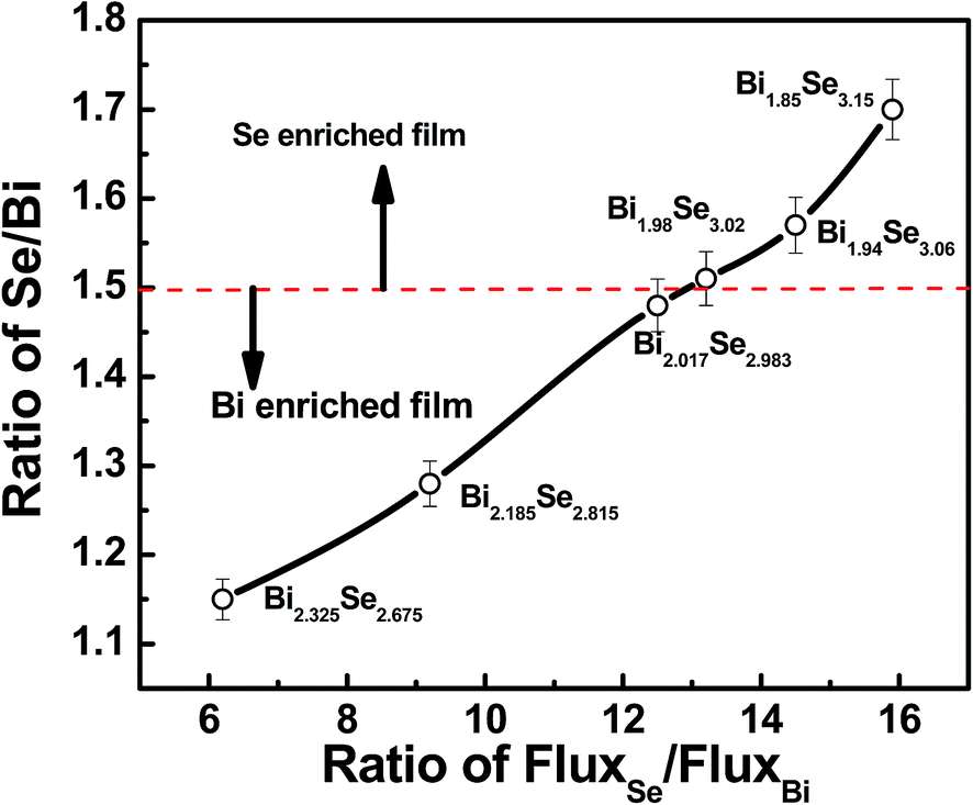 | ||
| Fig. 2 Dependence of Se/Bi ratio of grown films on the ratio of Se/Bi fluxes from the effusion cell. | ||
3.2. Grazing incidence X-ray reflectivity
The thickness of the stoichiometric bismuth selenide films, which were grown on SrTiO3 substrates was estimated by the grazing incidence X-ray reflectivity (GIXRR) spectrum i.e. specular reflectivity as a function of wave vector transfer q (= (4π/λ)sinθ, where θ is the incident angle and λ is the wavelength of the probe) and results are shown in Fig. 3. The reflectivity data has been fitted using a depth-dependent electron scattering length density (e-SLD) profile, that is,  , where N is the in-plane average of the number density, z is the film depth averaged over in-plane features and b is the electron scattering length.14 The estimated values of films thickness ∼10 nm, surface roughness ∼10.5 Å and the electron scattering length density ∼5.3 × 10⁻⁵ Å−2 were obtained from best-fit theoretical simulation of the data (shown by solid line in Fig. 3). The drop of e-SLD near films–air interface is assigned to the surface roughness of the films.
 | ||
| Fig. 3 X-ray reflectivity spectrum films for Bi2Se3 films grown on SrTiO3 substrate. Solid red line is the experimental fit to the data. Insert shows the depth profile of the electron scattering length density (e-SLD). | ||
3.3. Morphology, structure and low temperature charge transport
Fig. 4(a) and (b) shows the AFM images of the Bi2Se3 films grown on SrTiO3 and LaAlO3 substrates, which shows that both films exhibit granular surface morphology. The average surface roughnesses of the films grown on SrTiO3 and LaAlO3 were found to be ∼0.5 and ∼1.5 nm respectively. These roughness value for Bi2Se3 films closely matches with the average surface roughness of the SrTiO3 (roughness ∼0.4 nm) and LaAlO3 (roughness ∼ 1.1 nm) substrates respectively. X-ray diffraction data recorded for samples are plotted in Fig. 4(c). It may be noted that XRD data is plotted only in the 2θ in the range of 25–40° to avoid the high intensity XRD peak of the single crystal substrates. From the XRD data it can be seen that both samples are polycrystalline and the peaks in the XRD pattern can be indexed as orthorhombic Bi2Se3 (JCPDS: 77-2016). The grain size estimated (using Scherrer formula) from highest intensity (340) peak was respectively found to be 16.2 nm and 15.7 nm for the films grown on SrTiO3 and LaAlO3.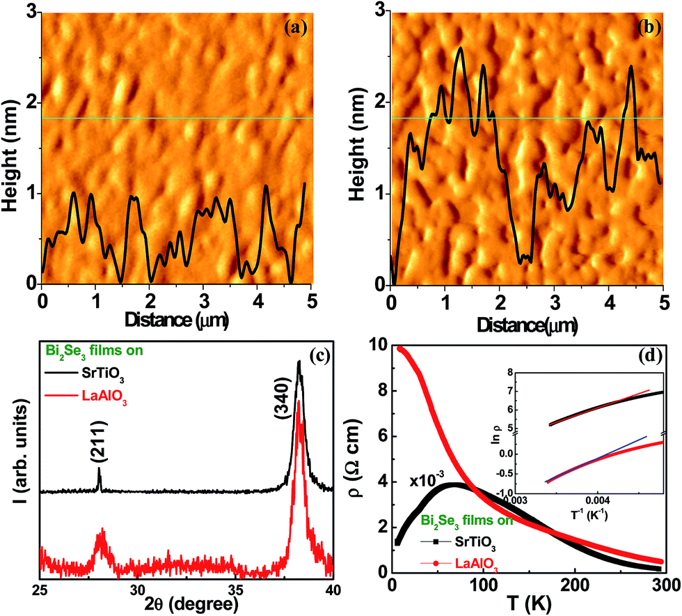 | ||
| Fig. 4 AFM images for Bi2Se3 films grown on (a) SrTiO3, (b) LaAlO3. Roughness profile shown in the AFM images is measured along the green line (c) X-ray diffraction pattern (d) temperature dependence of resistivity for Bi2Se3 films grown on SrTiO3, and LaAlO3 substrates. It may be noted that resistivity for the films grown on SrTiO3 substrate is multiplied by a factor of 10−3 to show the data's of both samples on same scale. Inset shows the inverse temperature dependence of resistivity of Bi2Se3 films. Straight line a fit to the data according to thermally activated conduction model. | ||
Fig. 4(d) shows the temperature dependence of resistivity (ρ) for Bi2Se3 films and from the data presented following inferences can be drawn: (i) the room temperature electrical resistivity of the films grown on SrTiO3 is nearly three order of magnitude higher as compared to that grown on LaAlO3 substrate. It may be noted that in Fig. 3(c), resistivity for the Bi2Se3 films grown on SrTiO3 substrate is intentionally multiplied by a factor of 10−3 to show the data of both samples in the same scale. (ii) Interestingly films grown on SrTiO3 substrate exhibit semiconductor to metal transition at around 68 K, while films prepared on LaAlO3 exhibit semiconducting behavior down to 5 K.
In bismuth selenide films the n-type electrical conductivity enhances with the deficiency of the selenium.13 As discussed earlier, the XPS result suggests that both films are stoichiometric hence both sample should have same extrinsic carrier concentration. XRD data suggested that both films exhibit same crystalline structure and similar grain size therefore it can be safely assumed that both samples may have similar charge carrier mobility. Based on these results the huge difference in the electrical resistivity of both films can be related to substrate and films interaction. It is to be noted that both SrTiO3 and LaAlO3 have similar perovskite structure. SrTiO3 single crystal consist of electrically neutral Sr2+O2− and Ti4+O2− layers, while for LaAlO3 the layers are polar i.e. positive for La3+O2− and negative for Al3+O22−.15 The surface of LaAlO3 single crystal is usually terminated with Al3+O2− and when a thin Bi2Se3 layer deposited on the top of such polar surface and it may release the electron into the Bi2Se3 films (near the LaAlO3 interface) for attaining the charge neutrality. Such a charge transfer from LaAlO3 surface is already reported at LaAlO3/SrTiO3 interface.16 We propose that the presence of an electron rich layer at LaAlO3/Bi2Se3 interface may be responsible for the high conductivity of the Bi2Se3 films.
As seen from Fig. 4(d), in the high temperature (250 K < T ≤ 300 K) region both films exhibit semiconducting behavior and ρ versus data for Bi2Se3 films grown on SrTiO3 and LaAlO3 substrates is fitted with the thermally activated hopping model ρ(T) = ρ(0)exp(−Δ/kT), which gives the value of activation energy (Δ) as 0.14 eV and 0.07 eV respectively for the films grown on SrTiO3 and LaAlO3 substrates.17 The higher value of activation energy for films grown on SrTiO3 also suggest that grain boundary energy barriers are more predominant in these films.
Now we discuss why the films prepared on SrTiO3 substrate exhibit metallic transition below 100 K. It is known that SrTiO3 substrate under goes a cubic to tetragonal structural transition with reduction in volume and an increase in c/a ratio (from 1 to 1.00056) i.e., in-plane compression of the unit cell around 100 K.18–20 The effect of this structural transition at low temperature must have an impact on the film–substrate interface and/or properties of ultra thin film grown on SrTiO3. This structural transition of SrTiO3 may facilitate the metallic transition in Bi2Se3 semiconducting film at low temperature. In order to further investigate the role of SrTiO3 substrate inducing the metallic transition in Bi2Se3 films, we have studied the temperature; thickness and electric field dependence of resistance of stoichiometric as well as non-stoichiometric bismuth selenide films and results are shown in Fig. 5. Fig. 5(a) shows the temperature dependence of the normalized resistance and several interesting features can be seen from this data such as: (i) for Bi2Se3 films, with increasing thickness from 10 nm to 20 nm the semiconducting to metallic transition temperature decreases from 68 K to 48 K and with further increase of films thickness up to ∼50 nm the metallic transition is vanished. (ii) Non-stoichiometric films that are selenium deficient (Bi2Se2.3) and selenium rich (Bi2Se3.1) films exhibit semiconducting temperature dependence in the entire temperature. From Fig. 5(b) it can be seen that for Bi2Se3 films of thickness ∼10 nm, semiconductor–metal transition temperature (TIM) depends on the applied bias and for bias <5 V, we do not see the metallic behavior. As seen from the inset of Fig. 5(b), nearly four times enhancement in TIM is seen when applied bias increases from 5 to 100 V.
 | ||
| Fig. 5 (a) Temperature dependence of normalized resistance for Bi2Se3 (stoichiometric) and Bi2Se2.3 (non-stoichiometric) films of different thickness grown on SrTiO3 substrate. (b) Temperature dependence of resistance taken at different bias for Bi2Se3 films of thickness ∼10 nm. Inset shows the bias dependence of semiconductor–metal transition temperature (TIM) for 10 nm thick Bi2Se3 films. | ||
It has been reported that oxygen deficiency in SrTiO3−δ causes the conversion of Ti4+ to Ti3+ and formation of defect level 25 meV below the conduction band and it serves as a donor level at room temperature.21 Such oxygen deficient SrTiO3−δ sample exhibit metallic or superconductivity at low temperatures.21–23 To confirm that whether the semiconductor to metal transition with lowering of temperature is purely arises from Bi2Se3 films and not from the SrTiO3 substrate, we have carried out following experiments: (i) SrTiO3 substrate was annealed under identical condition (at 300 °C for around 100 minutes, pressure ∼7 × 10⁻⁹ mbar) and in situ room temperature XPS data obtained [results obtained are shown in ESI (Fig. S1†)] suggest that before and after annealing the high resolution XPS spectra of Ti-2p, O-1s and Sr-3d. Looks exactly identical which suggest that during the annealing at 300 °C in ultra high vacuum the oxygen does not come out from the SrTiO3. Further electrical measurements were carried out on vacuum annealed SrTiO3 substrate and their room temperature electrical resistivity was found to be ∼4.5 × 10¹³ Ω cm (measured at 100 V). Such a high resistivity of the SrTiO3 substrate rules out their role in charge transport properties of Bi2Se3 thin films.
Typical temperature dependent current–voltage characteristics (J–V) characteristics of the Bi2Se3 films (thickness ∼10 nm) grown on SrTiO3 substrate were recorded in the bias range of 0–50 V, the results obtained is plotted in Fig. 6(a). It can be seen that J–V characteristics are linear in the temperature range of 300–200 K. The J–V data in the metallic state (i.e. at T < 70 K) shows (Fig. 6(b)) a peculiar behavior. It can be seen that in the bias range of 0–5 V, current is extremely low and for higher bias the current increases rapidly. The constant slope (∼4) of J–V curves (at high bias >10 V) along with slight variation with temperature indicates that field assisted hopping of charge carriers, according to this conductivity has an inverse square-root dependence i.e.  , where E0 is a related to materials parameter through the relation:
 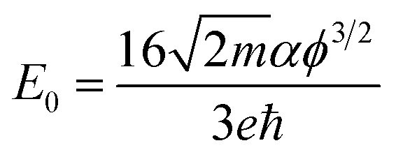 .24,25 Here ϕ is the energy barrier, and α is given by α = ln(p−1), where pN is the probability for forming N step tunneling path. As shown in inset of Fig. 5(b), the conductivity indeed varies as the inverse square-root of the field, confirming the field assisted tunneling of the charge carriers. From the least square fitting of the data shown in the inset of Fig. 6(b), the estimated ϕ is found to be 0.19 eV. Nearly similar value of the ϕ estimated from the low temperature data and the activation energy (∼0.14 eV) obtained from the high temperature resistivity data suggest that indeed the charge transport in these films is governed by the energy barrier present at the grain boundaries. It may be noted that Bi2Se3 films grown on LaAlO3 substrate exhibit linear current–voltage characteristics in the entire temperature range, which suggest that grain boundaries does not affect charge transport in these films.
 | ||
| Fig. 6 (a) Temperature dependent current–voltage (J–V) characteristics of Bi2Se3 films grown on SrTiO3 substrate. (b) Expanded view of (J–V) characteristics in the temperature range 1.5–50 K. Inset shows the plot of conductivity as a function of inverse square-root of the electric field in the temperature range of 1.5–50 K. | ||
In the light of the above detailed charge transport study, we propose that in-plane compression of the SrTiO3 substrate increases the grain to grain connectivity i.e. decreases in inter-grain space. In this situation, charge carrier can easily tunnel through the grain boundary region in the presence of high electric field. It is also obvious that the effect of compression of substrate will be dominant at the film–substrate interface and diminishes as the film thickness increases. Hence, for 20 nm thick Bi2Se3 films the semiconducting to metal transition shifted to lower temperature by 20 K in comparison to the 10 nm thick films and finally for 50 nm thick films metallic behavior is not observed in the entire temperature range. It is important to mention that non-stoichiometric (Bi2Se2.3) films exhibit room temperature resistivity of ∼13.3 Ω cm, which is attributed to the high electron concentration of n ∼ 8.5 × 1015 cm−3 (obtained from Hall measurement) that arises due to deficiency of Se. Hence for non-stoichiometric (Bi2Se2.3) films the effect of SrTiO3 compression on charge transport is not visible due to their low resistivity.
4. Conclusions
In summary, Bi2Se3 films of thickness ∼10 nm were grown on (100) SrTiO3 and (100) LaAlO3 single crystal substrates by MBE. The optimization of the Bi and Se fluxes from the effusion cells during the growth yield highly stoichiometric Bi2Se3 films. It has been observed that films grown on SrTiO3 substrate exhibit very high resistivity along with a semiconductor to metal like transition around 68 K with the lowering of temperature. Films prepared on LaAlO3 substrate exhibit semiconducting behavior in the entire temperature range. We propose that low temperature structural transition of SrTiO3 substrate, which yield compressive strain on the films facilitates the metal like transition by modifying the grain boundary characteristics.References
- Thermoelectrics Handbook, ed. D. M. Rowe, CRC Press, Boca Raton, FL, 1995 Search PubMed.
- A. Singh, S. Bhattacharya, C. Thinaharan, D. K. Aswal, S. K. Gupta, J. V. Yakhmi and K. Bhanumurthy, J. Phys. D: Appl. Phys., 2009, 42, 015502 CrossRef.
- R. Venkatasubramanian, E. Siivola, T. Colpitts and B. O'Quinn, Nature, 2001, 413, 597 CrossRef CAS PubMed.
- W. Liu, K. C. Lukas, K. McEnaney, S. Lee, Q. Zhang and C. P. Opeil, Energy Environ. Sci., 2013, 6, 552 CAS.
- H. Zhang, C. X. Liu, X. L. Qi, X. Dai, Z. F. Fang and S. C. Zhang, Nat. Phys., 2009, 5, 438 CrossRef CAS PubMed.
- L. Fu, C. L. Kane and E. Mele, Phys. Rev. Lett., 2007, 98, 106803 CrossRef.
- H. D. Li, Z. Y. Wang, X. Kan, X. Guo, H. T. He, Z. Wang, J. N. Wang, T. L. Wong, N. Wang and M. H. Xie, New J. Phys., 2010, 12, 103038 CrossRef.
- L. He, F. Xiu, Y. Wang, A. V. Fedorov, G. Huang, X. Kou, M. Lang, W. P. Beyerman, W. P. Zou, J. Zou and K. L. Wang, J. Appl. Phys., 2011, 109, 103702 CrossRef PubMed.
- L. He, X. Kou and K. L. Wang, Phys. Status Solidi RRL, 2013, 7, 50 CrossRef CAS PubMed.
- H. Katharina, B. Christoph, R. Diana, S. Jesse, T. Peter and L. H. Tjeng, PNAS, 2014, 111, 14979 CrossRef PubMed.
- A. Singh, S. Samanta, A. Kumar, A. K. Debnath, R. Prasad, P. Veerender, V. Balouria, D. K. Aswal and S. K. Gupta, Org. Electron., 2012, 13, 2600 CrossRef CAS PubMed.
- Q. Zhang, H. Qin, J. Teng, J. Guo, Q. Guo, X. Dai, Z. Fang and K. Wu, Appl. Phys. Lett., 2009, 95, 053114 CrossRef PubMed.
- P. Tabor, C. Keenan, S. Urazdhin and D. Lederman, Appl. Phys. Lett., 2011, 99, 013111 CrossRef PubMed.
- S. Singh, J. T. Haraldsen, J. Xiong, E. M. Choi, P. Lu, D. Yi, X.-D. Wen, J. Liu, H. Wang, Z. Bi, P. Yu, M. R. Fitzsimmons, J. L. MacManus-Driscoll, R. Ramesh, A. V. Balatsky, J.-X. Zhu and Q. X. Jia, Phys. Rev. Lett., 2014, 113, 047204 CrossRef.
- N. Nakagawa, H. Y. Hwang and D. A. Muller, Nat. Mater., 2006, 5, 204 CrossRef CAS PubMed.
- T. C. Asmara, A. Annadi, I. Santoso, P. K. Gogoi, A. Kotlov, H. M. Omer, M. Motapothula, M. B. H. Breese, M. Rübhausen, T. Venkatesan, Ariando and A. Rusydi, Nat. Commun., 2013 DOI:10.1038/ncomms4663.
- J. G. Checkelsky, Y. S. Hor, R. J. Cava and N. P. Ong, Phys. Rev. Lett., 2011, 106, 196801 CrossRef CAS.
- L. Cao, E. Sozontov and J. Zegenhagen, Phys. Status Solidi, 2000, 181, 387 CrossRef CAS.
- V. K. Vlasko-Vlasov, Y. K. Lin, D. J. Miller, U. Welp, G. W. Crabtree and V. K. Nikitenko, Phys. Rev. Lett., 2000, 84, 2239 CrossRef CAS.
- W. M. Lu, X. Wang, Z. Q. Liu, S. Dnar, A. Annadi, K. Gopinadhan, A. R. Barman, H. B. Su, T. Venkatesan and Ariando, Appl. Phys. Lett., 2011, 99, 172103 CrossRef PubMed.
- Z. Q. Liu, D. P. Leusink, X. Wang, W. M. Lü, K. Gopinadhan, Y. T. Lin, A. Annadi, Y. L. Zhao, X. H. Huang, A. Srivastva, S. Dhar, T. Venkatesan and Ariando, Phys. Rev. Lett., 2011, 107, 146802 CrossRef CAS.
- M. Jourdan and H. Adrian, Phys. C, 2003, 388–389, 509 CrossRef CAS.
- R. Di Capua, M. Radovic, G. M. De Luca, I. Maggio-Aprile, F. Miletto Granozio, N. C. Plumb, Z. Ristic, U. Scotti di Uccio, R. Vaglio and M. Salluzzo, Phys. Rev. B: Condens. Matter Mater. Phys., 2012, 86, 155425 CrossRef.
- A. S. Dhoot, G. M. Wang, D. Moses and A. J. Heeger, Phys. Rev. Lett., 2006, 96, 246403 CrossRef CAS.
- J. H. Wei, Y. L. Gao and X. R. Wang, Appl. Phys. Lett., 2009, 94, 073301 CrossRef PubMed.
Footnote |
| † Electronic supplementary information (ESI) available. See DOI: 10.1039/c5ra17949a |
| This journal is © The Royal Society of Chemistry 2015 |