
Selective extraction of metallic arc-discharged single-walled carbon nanotubes by a water soluble polymethylsilane derivative†
Jinling Gaoab,
Yao Huanga and
Yongfu Lian*a
aKey Laboratory of Functional Inorganic Material Chemistry, Ministry of Education, School of Chemistry and Materials Science, Heilongjiang University, Harbin 150080, China. E-mail: chyflian@hlju.edu.cn
bCollage of Science, Heilongjiang Bayi Agricultural University, Daqing, 163319, China
First published on 13th November 2015
Abstract
Water soluble polymethyl(1-undecylic acidyl)silane, synthesized by the hydrosilylation of 10-undecylenic acid with polymethylsilane catalyzed by 2,2′-azobisisbutyronitrile, demonstrates selective extraction ability toward metallic single-walled carbon nanotubes (SWNTs) produced by the arc discharge method. After heating in air at a temperature of 673 K and treatment with concentrated hydrochloric acid, the arc-discharged SWNTs are ultrasonically dispersed in an aqueous solution of polymethyl(1-undecylic acidyl)silane. Such obtained dispersions are subjected to ultracentrifugation, and then the supernatant is collected. Optical absorption spectra show that the supernatant is enriched in the metallic SWNTs. Moreover, Raman spectra confirm the selective extraction of (14,2), (15,0), (13,1), (12,3) and (19,1) metallic SWNTs, which have larger diameters and smaller chiral angles than those reported previously. Additionally, FT-IR spectroscopy and Raman scattering evidence the charge transfer between polymethyl(1-undecylic acidyl)silane and SWNTs. It is conjectured that polymethyl(1-undecylic acidyl)silane could wrap chiral-index-selectively onto SWNTs through a fairly weak CH–π interaction. Thus, we believe that the stiffness and length of main chains and side chains as well as the charge state of the polymethylsilane derivative play vital roles in the selective extraction of SWNTs.
1. Introduction
Single-walled carbon nanotubes (SWNTs) have attracted considerable attention because of their unique electrical, mechanical, thermal and optical properties, which are significant for all kinds of potential technological applications.1–9 Usually, as-synthesized SWNTs form large bundles containing many kinds of species. In order to obtain better materials performance, researchers have dispersed as-synthesized SWNT samples in many solubilizing agents and separated them in line with their length, diameter, metallicity, (n,m) structure and handedness by electrophoresis,10,11 centrifugation,12–14 chromatography,15–20 selective solubilization21–24 and selective reaction.25–27Normally, SWNTs are solubilized or individually dispersed either by covalent chemical functionalization or by non-covalent dispersion with the assistance of biological macromolecules, surfactants, ionic liquids and polymers.28–30 Among the polymers applied, nonaromatic polyvinylpyrrolidone, polystyrenesulfonate, poly(allylamine) and α-helical amphiphilic peptides show dispersion ability towards SWNTs in aqueous media, and semiconducting SWNTs are selectively extracted out.31–33 On the other hand, π-conjugated polymers particularly polyfluorene (PFO) homo- and co-polymers are evidenced to be able to extract selectively specific semiconducting SWNTs.34 It should be noted that PFO itself shows effective interactions only with smaller diameter SWNTs (0.8–1.2 nm), and poly(dialkylfluorene)s with increasing lengths of alkyl chain can interact with nanotubes of larger diameter up to 1.5 nm.35 Moreover, poly(dioctylfluorene-alt-benzothiadiazole) (F8BT) and the copolymer of dioctylfluorene and bipyridine units (PFO-BPy) demonstrate selective extraction towards semiconducting SWNTs with specific chiral indexes of (15,4)36 and (6,5),37 respectively. Meanwhile, poly[di(N,N-dimethylaminopropyl)fluorene] (PFDMA) and poly[di(N,N,N-trimethylammoniumpropyl)fluorene dibromide] (PFAB) have proved to be able to extract selectively semiconducting (6,5) and (7,5) SWNTs.38 Recently, it has been found that copolymers composed of fluorene or aryleneethynylene and chiral binaphthol units exhibit judicious separation of left- and right-handed semiconducting SWNTs.39,40 Additionally, regioregular poly(3-alkylthiophene)s (rr-P3ATs) including rr-P3DT (alkyl = n-decyl) and rr-P3DDT (alkyl = n-dodecyl) are reported to be also applicable to the selective extraction of semiconducting HiPCO and CoMoCAT nanotubes.41
Polysilane is a typical nonaromatic σ-conjugated polymer, composed of alkyl side chains attached to the silicon-catenated main chain. From the viewpoint of electronic structure, polysilane can be regarded as a quasi-one-dimensional material, due to the delocalized σ-conjugated electrons along the Si main chain.42,43 Naito et al. reported the solubilization of CoMoCAT SWNTs in THF by a series of poly(dialkylsilane)s.44,45 It was found that the polysilanes bearing methyl and n-alkyl side chains are able to solubilize CoMoCAT SWNTs in THF, resulting in the enrichment of semiconducting (7,6) and (9,4) SWNTs with a diamater of ca. 0.9 nm.
SWNTs can be produced in large quantities by arc discharge,46 chemical vapor deposition,47 laser ablation,48 the CoMoCAT process,49 and high-pressure carbon monoxide disproportionation (HiPCO).50 All these processes yield mixtures of semiconducting and metallic SWNTs with variations in the distribution of the (n,m) indices within certain diameter ranges. CoMoCAT and HiPCO SWNTs are employed widely in the formation of stable dispersion of SWNTs. They are formed at a temperature ca. 1273 K and with diameters distributed from 0.7 to 1.2 nm. Meanwhile, arc-discharged SWNTs are generated at a temperature higher than the evaporating point of graphite, and this process yields a random distribution of metallic and semiconducting SWNTs with diameters ranging from 0.8 to 2.0 nm. In comparison with the others, arc-discharged SWNTs are longer and straighter with fewer defects and usually tend to form large bundles due to the stronger van der Waals interactions, which make them more difficult to be solubilized.51 To date there are no reports on the selective solubilization of arc-discharged SWNTs with polymers, neither in line with their length, diameter, metallicity, (n,m) structure nor handedness.
In this study, a water soluble polymethylsilane derivative (Scheme 1) is firstly applied to the selective extraction of SWNTs. Optical absorption spectroscopy and Raman spectroscopy confirm the selective extraction of metallic arc-discharged SWNTs. Moreover, those metallic SWNTs are greatly enriched, indicating the first successful isolation of metallic SWNTs with large diameters and small chiral angles.
 | ||
| Scheme 1 Preparation of water soluble polymethyl(1-undecylic acidyl)silane. | ||
2. Experimental
2.1 Preparation and purification of SWNTs
As-synthesized SWNTs were prepared by an improved arc discharge procedure.46 The anode was an Ø 6 × 120 mm Specpure graphite rod drilled with an Ø 4 × 100 mm hole and filled with a powdered mixture of graphite and catalysts including Y–Ni alloy and Fe–S compound. The cathode was a 40 × 40 mm graphite block. An arc was generated with an electric current of 100 A under a helium atmosphere of 500 Torr. After cooling down, as synthesized SWNTs were collected from the arc discharge chamber.The as synthesized SWNTs were thermally treated at 673 K for 3 h in an air atmosphere to burn out amorphous carbons, and then soaked in concentrated hydrochloric acid for 24 h to remove metal catalysts. After washing with a large amount of water and dried, the product was supersonically dispersed in 1% (wt/v) aqueous sodium deoxycholate solution. The obtained dispersion was subjected to centrifugation at a rotation speed of 15![[thin space (1/6-em)]](https://www.rsc.org/images/entities/char_2009.gif) 000 rpm for 2 h at 10 °C, and the supernatant above 80% was collected (named DOC-SWNTs).
000 rpm for 2 h at 10 °C, and the supernatant above 80% was collected (named DOC-SWNTs).
2.2 Synthesis of polymethyl(1-undecylic acidyl)silane
The water soluble polymethyl(1-undecylic acidyl)silane, was synthesized by the following two steps (Scheme 1). Polymethylsilane was firstly prepared by a sodium-mediated Wurtz reductive coupling of dichloromethylsilane in refluxing toluene.43 Secondly, polymethyl(1-undecylic acidyl)silane was synthesized by the hydrosilylation of 10-undecylenic acid with polymethylsilane using 2,2′-azobisisbutyronitrile (AIBN) as initiator.52 4.4 g polymethylsilane (containing 0.1 mol Si–H) and 0.4 g 2,2′-azobisisbutyronitrile were dissolved in 80 ml THF in a three-necked flask. After dissolving in 20 ml THF, 18.4 g 10-undecylenic acid (0.1 mol) was added drop by drop at the reflux temperature of THF under the aegis of highly pure nitrogen. The reactant mixture was refluxed for 12 h at 68 °C, and then filtered with normal filter paper. The filtrate was evaporated with a rotary evaporator to remove THF solvent, and then extracted with hexane and separated several times with a separating funnel to get the purified product. Such prepared polymethyl(1-undecylic acidyl)silane is a yellow viscous liquid, soluble in alkaline water, toluene, THF and ethanol.2.3 Selective extraction and isolation of SWNTs
In a typical experiment, 10 mg HCl-treated SWNTs were ultrasonically (Sonics, VCX 750, Vibra-cell, USA) dispersed in 100 ml alkaline aqueous solution of polymethy(1-undecylic acidyl)silane 1% (wt/v) (pH = 8) for 12 h at a temperature of 10 °C. The resulting dispersion was then centrifuged with an angle rotor (P70AT2, CP70MX, Hitachi KokiCo.) at a rotation speed of 15000 rpm for 2 h, and the supernatant above 80% was collected carefully. After evaporation with a rotary evaporator, a complex of polymethy(1-undecylic acidyl)silane and SWNTs was obtained.
2.4 Characterization methods
3. Results and discussion
3.1 The formation of polymethyl(1-undecylic acidyl)silane
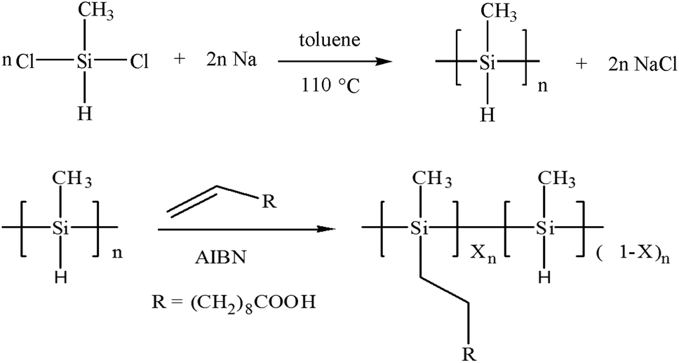
Shown in Fig. 1 are the FT-IR spectra of polymethylsilane, 10-undecylenic acid, and polymethyl(1-undecylic acidyl)silane. The absorption band of 2100 cm−1 observed in Fig. 1a is assigned to the stretching vibration of the Si–H bond, the characteristic IR absorption band of polymethylsilane, and the absorption band of 1620 cm−1 observed in Fig. 1b is ascribed to the stretching vibration of the C![[double bond, length as m-dash]](https://www.rsc.org/images/entities/char_e001.gif) C bond. It can be seen from Fig. 1c that the characteristic IR absorption band of polymethylsilane is significantly softened in comparison with that in Fig. 1a, whereas, the stretching vibration band of CC bond has completely disappeared. Thus, it is concluded that the hydrosilylation of 10-undecylenic acid with polymethylsilane occurs between the Si–H bonds in polymethylsilane and the CC bond in 10-undecenoic acid, and that the side chain of 10-undecylenic acid is attached to the main chain of polymethylsilane through an anti-Markovnikov addition reaction. With the formation of polymethyl(1-undecylic acidyl)silane, the molecular chain of polymethylsilane is unfolded,42 and the cross-linking reactions among Si–H bond are hindered. Particularly, the hydrophilic –COOH groups in the side chain make the polymethylsilane derivative soluble in water.
C bond. It can be seen from Fig. 1c that the characteristic IR absorption band of polymethylsilane is significantly softened in comparison with that in Fig. 1a, whereas, the stretching vibration band of CC bond has completely disappeared. Thus, it is concluded that the hydrosilylation of 10-undecylenic acid with polymethylsilane occurs between the Si–H bonds in polymethylsilane and the CC bond in 10-undecenoic acid, and that the side chain of 10-undecylenic acid is attached to the main chain of polymethylsilane through an anti-Markovnikov addition reaction. With the formation of polymethyl(1-undecylic acidyl)silane, the molecular chain of polymethylsilane is unfolded,42 and the cross-linking reactions among Si–H bond are hindered. Particularly, the hydrophilic –COOH groups in the side chain make the polymethylsilane derivative soluble in water.
 | ||
| Fig. 1 FT-IR spectra of polymethylsilane (a), 10-undecylenic acid (b), and polymethyl(1-undecylic acidyl)silane (c). | ||
3.2 The disperse ability of polymethyl(1-undecylic acidyl)silane towards SWNTs
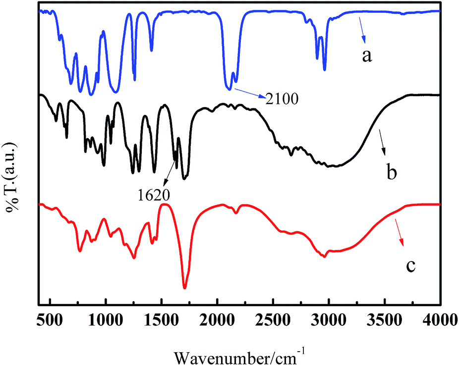
Fig. 2 demonstrates the photographs of SWNTs dispersed in water, the aqueous solutions of polymethyl(1-undecylic acidyl)silane, and the aqueous solutions of DOC. It can be seen from Fig. 2b and c that black dispersions of SWNTs are formed with the assistance of polymethyl(1-undecylic acidyl)silane and DOC, respectively. In sharp contrast, some fine black particles are visible in Fig. 2a. After setting for 30 days, the dispersions of SWNTs with the polymethyl(1-undecylic acidyl)silane and DOC show a much strong stability (see Fig. 2e and f), whereas the SWNTs dispersed in water undergo serious agglomeration and precipitate completely. It is obvious that polymethyl(1-undecylic acidyl)silane demonstrates a similar dispersion ability towards SWNTs as does DOC. | ||
| Fig. 2 Photographs of SWNTs dispersed in water (a), the aqueous solution of polymethyl(1-undecylic acidyl)silane (b), and the aqueous solution of DOC (c). (d), (e) and (f) are taken after (a), (b) and (c) setting for 30 days, respectively. | ||
Microstructural characterization of the complex of polymethyl(1-undecylic acidyl)silane and SWNTs was performed using AFM. The typical AFM images of the complex of polymethyl(1-undecylic acidyl)silane and SWNTs (Fig. 3), clearly show the presence of many long filamentous structures. These structures are ascribed to the complex of polymethyl(1-undecylic acidyl)silane and SWNTs, in which very straight SWNTs are observed with an average length of about 1.8 μm. The dome-like structures observed on the substrate are considered to be composed of molecular aggregates of polymethyl(1-undecylic acidyl)silane, which consists of three distinct parts, i.e. a horizontally self-assembled monolayer (0.8 nm), a transition state (2 nm) and vertical alignment (8.0 nm).53,54
 | ||
| Fig. 3 AFM images of the complex of polymethyl(1-undecylic acidyl)silane and SWNTs. | ||
From Fig. 3, it can be seen that the complexes of SWNTs and polymethyl(1-undecylic acidyl)silane coexist with free polymethyl(1-undecylic acidyl)silane in the supernatant. Moreover, SWNTs are observed to be well coated by polymethyl(1-undecylic acidyl)silane with varying thickness, and are well dispersed. Height analysis in different regions (indicated by white solid lines in the image) produced values ranging from 6 to 10 nm. Considering the varying orientation of the polysilane derivative and the varying thickness of the coating on SWNTs, it is reasonable for us to assign the SWNTs observed here as individuals. Therefore, the AFM image evidences that polymethyl(1-undecylic acidyl)silane strongly interacts with SWNTs and is able to exfoliate them into individuals or very small bundles in water, leading to the good dispersion ability of polymethyl(1-undecylic acidyl)silane towards SWNTs.
To provide further support for the good dispersion ability of polymethyl(1-undecylic acidyl)silane towards SWNTs, SEM observation was carried out. Shown in Fig. 4 is the SEM image of the complex of polymethyl(1-undecylic acidyl)silane and SWNTs dropped and dried on an Si wafer. Because of the bad electronic conductivity of polymethyl(1-undecylic acidyl)silane unevenly coated on SWNTs, the SEM image of the complex is usually not as clear as those of naked SWNTs. It is obvious that small bundles of SWNTs are observed to be coated with blurred materials and the branches are cross-linked to a certain extent. It is no doubt that these blurred materials are self-assembled polymethyl(1-undecylic acidyl)silane, indicating that they are wrapped onto the surface of carbon nanotubes. The branched, cross-linked appearance is assumed to be formed from these well dispersed individual or thin bundles of SWNTs. During the preparation of SEM samples, they aggregate into larger bundles driven by the self-assembly of polymethyl(1-undecylic acidyl)silane, and are observed as rigid structures.
 | ||
| Fig. 4 SEM image of the complex of polymethyl(1-undecylic acidyl)silane and SWNTs. | ||
Additionally, the SEM image shown in Fig. 4 is recorded with the SWNTs freshly dispersed in an aqueous solution of polymethyl(1-undecylic acidyl)silane (see Fig. 2b). After the SWNTs freshly dispersed in the aqueous solutions of polymethyl(1-undecylic acidyl)silane were set for 30 days, the diameter of the SWNTs bundles increases to as large as 120 to 250 nm (see Fig. S2†). It is estimated that such strong self-assembly would influence its selective dispersion ability toward SWNTs to some extent.
3.3 The selective extraction of metallic SWNTs
UV-vis-NIR spectroscopy is sensitive to the presence of metallic and semiconducting SWNTs. Shown in Fig. 5 are the vis-NIR absorption spectra of DOC-SWNTs (a), and the complex of SWNTs and polymethyl(1-undecylic acidyl)silane (b), solubilized in water. In order to avoid the disturbance from water absorption, the vis-NIR absorption spectra are recorded in the wavelength range from 400 to 1400 nm. For arc-discharged SWNTs, the absorption bands in the 600–800, 850–1290 nm regions are attributed to the first van Hove transition of metallic SWNTs (M11), and the second van Hove transition of semiconducting SWNTs (S22). It could be seen from Fig. 5 that the absorption curve b demonstrates more fine features than curve a, resulting from the better dispersion ability of polymethyl(1-undecylic acidyl)silane towards SWNTs than that of DOC. As a matter of fact, the distinguishable and intense peaks in Fig. 5b indicate that the arc-discharged SWNTs are individually solubilized in the aqueous solution of polymethyl(1-undecylic acidyl)silane. Though DOC is a good agent for the solubilization of SWNTs, it does not show any selectivity for any special types of carbon nanotubes. Therefore DOC-SWNTs make good contrasting objects for the evaluation of the selective extraction of polymethyl(1-undecylic acidyl)silane towards SWNTs. As illustrated in Fig. 5, the band area in the M11 region increases from curve a to curve b, whereas the band area in the S22 region decreases in the same order. It appears that polymethyl(1-undecylic acidyl)silane preferentially extracts metallic SWNTs, leading to the supernatants being enriched in metallic species and suppressed in semiconducting ones. Moreover, it is also observed that the average absorption is blue-shifted from curve a to curve b for both the M11 band and the S22 band. We speculate that such a blue shift is due to the selective extraction of polymethyl(1-undecylic acidyl)silane towards SWNTs with varying diameters or even with varying (n,m) structures.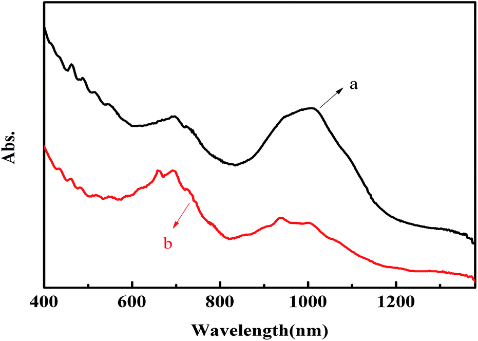 | ||
| Fig. 5 Normalized vis-NIR spectra of DOC-SWNTs (a), and the complex of polymethyl(1-undecylic acidyl)silane and SWNTs (b). | ||
An estimate of the relative abundance of metallic or semiconducting SWNTs can be derived by integrating the peak areas in the M11 and S22 regions in line with the method proposed by Haddon et al.55 As show in Fig. 6, in the M11 region the ratios of the areas under the curves after and before baseline subtraction, AA(S)/AA(T) are 0.060 and 0.154 for DOC-SWNTs and for the complex of polymethyl(1-undecylic acidyl)silane and SWNTs, respectively. Therefore, the relative carbonaceous purity of the metallic SWNTs in complex of SWNTs and polymethyl(1-undecylic acidyl)silane to that in DOC-SWNTs is about 2.567 (0.154/0.060). Similarly, in the S22 region the ratios of the areas under the curves after and before baseline subtraction, AA(S)/AA(T) are 0.191 and 0.138 for DOC-SWNTs and for the complex of polymethyl(1-undecylic acidyl)silane and SWNTs, respectively. Therefore, the relative carbonaceous purity of the semiconducting SWNTs in complexes of SWNTs and polymethyl(1-undecylic acidyl)silane to that in DOC-SWNTs is about 0.723 (0.138/0.191). Thus, the content of metallic SWNTs in the complex of polymethyl(1-undecylic acidyl)silane and SWNTs is about 3.55 (2.567/0.723) times of that of semiconducting ones, highlighting the selective extracting ability of polymethyl(1-undecylic acidyl)silane towards metallic SWNTs.
 | ||
| Fig. 6 The relative purity of DOC-SWNTs (upper) and the complex of polymethyl(1-undecylic acidyl)silane and SWNTs (lower) based on the vis-NIR absorption spectra. | ||
It is well known that Raman spectroscopy is a powerful technique to characterize carbon materials. To investigate further the special selectivity of polymethyl(1-undecylic acidyl)silane towards metallic SWNTs, resonant Raman spectroscopy was applied under excitation at 488, 514, 633, and 785 nm, respectively, which will bring varying metallic and semiconducting arc-discharged SWNTs into resonant scattering. The energy of the species interband electronic transition depends on the diameter and metallicity of SWNTs, and the diameters of SWNTs are inversely proportional to radial breathing modes (RBM) peaks in the 100–400 cm−1 range.
Shown in Fig. 7 are the normalized Raman spectra of DOC-SWNTs and the complex of polymethyl(1-undecylic acidyl)silane and SWNTs under excitation at 488, 514, 633, and 785 nm, respectively. The Raman spectra are normalized at the G+ band (around 1590 cm−1). According to the reference Kataura plot and the wavelength of the excitation laser, the RBM peaks in these Raman spectra are assigned to SWNTs species. In the 633 nm excitation spectrum (Fig. 7a), the RBM peaks appearing in the wavenumber range of 154–201 cm−1 are due to metallic SWNTs and those appearing in the wavenumber range of 201–240 cm−1 are due to semiconducting ones. It can be seen that the DOC-SWNTs show two peaks in the wavenumber range of 154–201 cm−1 (173 cm−1 and 189 cm−1) and one prominent peak in the range of 201–240 cm−1 (216 cm−1), assignable to carbon nanotubes with indices of (14,2), (15,0) and (11,1), respectively. Whereas the complex of polymethyl(1-undecylic acidyl)silane and SWNTs only show two strong peaks in the wavenumber range of 154–201 cm−1 (169 cm−1 and 185 cm−1) assigned to carbon nanotubes with indices of (14,2) and (15,0), and no discernable peaks are observed in the range of 201–240 cm−1. Fig. 7c shows the Raman RBM spectra with 488 nm excitation. The peaks from 194 to 221 cm−1 are ascribed to metallic and those from 140 to 194 cm−1 to semiconducting SWNTs. It can be seen that the DOC-SWNTs show one prominent peak in the range of 140–194 cm−1 (180 cm−1), assignable to carbon nanotubes with indices of (15,4). However, the complex of polymethyl(1-undecylic acidyl)silane and SWNTs show one strong peak in the wavenumber range of 194–221 cm−1 (213 cm−1) assigned to carbon nanotubes with indices of (13,1). Fig. 7e shows the Raman RBM spectra with 514 nm excitation. The peaks from 189 to 221 cm−1 are ascribed to metallic and those from 152 to 189 cm−1 to semiconducting SWNTs. It can be seen that the DOC-SWNTs show one prominent peak in the range of 152–189 cm−1 (179 cm−1), assignable to carbon nanotubes with indices of (11,9), whereas the complex of polymethyl(1-undecylic acidyl)silane and SWNTs shows one strong peak in the wavenumber range of 189–221 cm−1 (197 cm−1) assigned to carbon nanotubes with indices of (12,3). Fig. 7g shows the Raman RBM spectra with 785 nm excitation. The peaks from 122 to 151 cm−1 are ascribed to metallic and those from 151 to 190 cm−1 to semiconducting SWNTs. It can be seen that the DOC-SWNTs show one prominent peak in the range of 151–190 cm−1 (161 cm−1), assignable to carbon nanotubes with indices of (13,3), whereas the complex of polymethyl(1-undecylic acidyl)silane and SWNTs shows one strong peak in the wavenumber range of 122–151 cm−1 (143 cm−1) assigned to carbon nanotubes with indices of (19,1). The polymethyl(1-undecylic acidyl)silane shows selectively extraction ability toward metallic carbon nanotubes with indices of (14,2), (15,0) with 633 nm excitation, (13,1), (12,3), (19,1) with 488 nm, 514 nm and 785 nm excitation, respectively. Therefore, it is concluded that polymethyl(1-undecylic acidyl)silane could selectively extract metallic carbon nanotubes and discriminate semiconducting species, consistent with the results of vis-NIR characterization.
 | ||
| Fig. 7 Raman spectra of DOC-SWNTs (1) and the complex of polymethyl(1-undecylic acidyl)silane and SWNTs (2) in the ranges of 100–300 cm−1 (a, c, e and g) and 1000–2000 cm−1 (b, d, f and h), respectively. | ||
The G band of SWNTs is actually composed of double peaks, i.e., the lower broad G− band (1520–1560 cm−1) and the upper sharp G+ band (around 1590 cm−1). According to Yi et al., G− and G+ bands indicate the presence of metallic and semiconducting SWNTs, respectively,56 and the metallic SWNTs normally show the asymmetric and wider Breit–Wigner–Fano (BWF) satellite band close to the upper G band.57 It can be seen from Fig. 7b, d, f and h that the G− band of the complex of polymethyl(1-undecylic acidyl)silane and SWNTs widens because of an elevated intensity relative to that of DOC-SWNTs. From the viewpoint of metallicity, the wider and more pronounced BWF feature means that the complex of polymethyl(1-undecylic acidyl)silane and SWNTs is enriched in metallic species, evidencing the special selectivity of polymethyl(1-undecylic acidyl)silane towards metallic SWNTs.
3.4 Formation of the electron donor–acceptor complex between polymethyl(1-undecylic acidyl)silane and metallic-SWNTs
FT-IR spectroscopy is applied to the investigation of the charge transfer between polymethyl(1-undecylic acidyl)silane and SWNTs. Shown in Fig. 8 are the FT-IR spectra of polymethyl(1-undecylic acidyl)silane and the polymethyl(1-undecylic acidyl)silane–SWNTs complex. It can be seen that the Si–C characteristic absorption peak red-shifts from 762 cm−1 in the polymethyl(1-undecylic acidyl)silane sample to 670 cm−1 in the polymethyl(1-undecylic acidyl)silane–SWNTs complex. The weakness of Si–C bonds is ascribed to a result of the charge transfer from the SWNTs to the partial occupation of the low lying antibonding acceptor orbital58 of polymethyl(1-undecylic acidyl)silane. Additionally, in comparison with those observed for polymethyl(1-undecylic acidyl)silane the other FT-IR characteristic features are also red-shifted, because of the charge transfer in the polymethyl(1-undecylic acidyl)silane–SWNTs complex. | ||
| Fig. 8 FT-IR spectra of polymethyl(1-undecylic acidyl)silane (a) and the complex of polymethyl(1-undecylic acidyl)silane–SWNTs (b). | ||
Moreover, Raman spectroscopy could probe the impact of charge transfer on the electronic structures of the doped SWNTs. According to Wise et al.,58 removing charge from SWNTs would result in an upshift in the G+ band peak around 1592 cm−1, while adding charge to SWNTs results in a downshift. It can be seen from the inset of Fig. 7b, d, f and h that the G+ band is upshifted to 1596 cm−1, 1597 cm−1, 1604 cm−1, 1604 cm−1 for DOC-SWNTs and to 1601 cm−1, 1604 cm−1, 1609 cm−1, 1610 cm−1 for the polymethyl(1-undecylic acidyl)silane–SWNTs complex. Obviously, the upshift in the G+ band peak is a result of the charge transfer from SWNTs to DOC or to polymethyl(1-undecylic acidyl)silane. A larger upshift in the G+ band peak indicates a greater amount of charge transferred. Therefore, it is concluded that more charge is transferred to polymethyl(1-undecylic acidyl)silane than to DOC from SWNTs.
The experimentally derived work function, the negative of the Fermi level, is 4.8–5.0 eV for metallic or small band gap semiconducting SWNTs.59,60 There are some free electrons at the Fermi levels of metallic SWNTs, whereas the electrons are bounded in the low lying valence band for semiconducting ones. Thus, the charge transfer from metallic SWNTs to polymethyl(1-undecylic acidyl)silane is more efficient than that from it’s semiconducting counterpart, leading to the successful formation of the complex between polymethyl(1-undecylic acidyl)silane and metallic SWNTs. The selective extraction of metallic SWNTs with polymethyl(1-undecylic acidyl)silane is a result of the formation of their electron donor–acceptor complex.
Naito et al.44,45 investigated the polymer wrapping behaviors of poly(dialkylsilane)s around SWNTs, and concluded that the stiffness and conformation played an essential role in the wrapping of poly(disilane)s onto SWNTs. As a matter of fact, the stiffness and conformation of poly(dialkylsilane)s are largely decided by the alkyl side chains. The dome-like structures observed in Fig. 3 reflect that the random-coiled polymethyl(1-undecylic acidyl)silane is flexible,61 and it is reasonable to assume that polymethyl(1-undecylic acidyl)silane is successfully wrapped onto the arc-discharged SWNTs to form a stable complex. After wrapping the plane of the dihedral angle of the Si main chain placed almost perpendicular to the grapheme surface of SWNTs, with its side chains (methyl and 1-undecylic acidyl) adopting a nearly all-trans zigzag conformation to fit the surface curvatures of the SWNTs. Such geometric distortion of polymethyl(1-undecylic acidyl)silane should play a crucial role in the stabilisation of its electron donor–acceptor complex with SWNTs.
From Fig. 8 it can be observed that the stretching bands of CH2 and CH3 at 2800–3100 cm−1 are downshifted 12–15 cm−1, indicating the existence of CH–π interactions62 among the linear alkyl side chains of polymethyl(1-undecylic acidyl)silane and the curved grapheme surface of SWNTs.45 If the main Si chain and the linear side chains of polymethyl(1-undecylic acidyl)silane are aligned respectively in the axial and radial directions of SWNTs, the side chains methyl and 1-undecylic acidyl might form a circle tightly attached onto SWNTs through the above CH–π interactions. In this situation, the diameter of a such formed circle ought to match those of wrapped SWNTs to some extent. Therefore, the length of the linear side chains of polymethyl(1-undecylic acidyl)silane endows selective wrapping to SWNTs with specific diameters.
4. Conclusion
A water soluble polymethylsilane derivative, polymethyl(1-undecylic acidyl)silane, is synthesized by the hydrosilylation of 10-undecylenic acid. Spectroscopic characterizations by vis-NIR and Raman confirm that polymethyl(1-undecylic acidyl)silane displays selective extraction towards arc-discharged metallic SWNTs through a simple sonication and centrifugation process. FT-IR and Raman spectra prove the charge transfer from metallic SWNTs to polymethyl(1-undecylic acidyl)silane, leading to the formation of the donor–acceptor complex between polymethyl(1-undecylic acidyl)silane and metallic SWNTs. Moreover, the side chains of polymethyl(1-undecylic acidyl)silane are wrapped onto SWNTs by the accumulation of multiple CH–π interactions. The diameters of the extracted SWNTs are correlated with the lengths of side chains (methyl and 1-undecylic acidyl). Thus, larger diameters and small chiral angles metallic SWNTs are selectively extracted by polymethyl(1-undecylic acidyl)silane.It is expected that the polymethyl(1-undecylic acidyl)silane closely wrapped metallic SWNTs might be a good electronic cable for nanodevices, and they could also be used for nanostorage after sputtering with a thin layer of metal.
Acknowledgements
This work was supported by the National Natural Science Foundation of China (Grant No. 51572071, 21271067), and Program for Innovative Research Team in University (Grant No. IRT-1237), Ministry of Education, China.Notes and references
- Q. Cao, H. S. Kim, N. Pimparkar, J. P. Kulkarni, C. Wang, M. Shim, K. Roy, M. A. Alam and J. A. Rogers, Nature, 2008, 454, 495–500 CrossRef CAS PubMed.
- A. Thess, R. Lee, P. Nikolaev, H. J. Dai, P. Petit, J. Robert, C. H. Xu, Y. H. Lee, S. G. Kim and R. E. Smalley, Science, 1996, 273, 483–487 CAS.
- N. Rouhi, D. Jain and P. Burke, ACS Nano, 2011, 5, 8471–8487 CrossRef CAS PubMed.
- C. Wang, J. Chien, K. Takei, T. Takahashi, J. Nah, A. M. Niknejad and A. Javey, Nano Lett., 2012, 12, 1527–1533 CrossRef CAS PubMed.
- M. E. Roberts, M. C. LeMieux and Z. Bao, ACS Nano, 2009, 3, 3287–3293 CrossRef CAS PubMed.
- R. J. Chen, H. C. Choi, S. Bangsaruntip, E. Yenilmez, X. Tang, Q. Wang, Y. L. Chang and H. Dai, J. Am. Chem. Soc., 2004, 126, 1563–1568 CrossRef CAS PubMed.
- D. Zhang, K. Ryu, X. Liu, E. Polikarpov, J. Ly, M. E. Tompson and C. Zhou, Nano Lett., 2006, 6, 1880–1886 CrossRef CAS PubMed.
- L. Hu, D. S. Hecht and G. Gruner, Chem. Rev., 2010, 110, 5790–5844 CrossRef CAS PubMed.
- S. L. Hellstrom, H. W. Lee and Z. Bao, ACS Nano, 2009, 3, 1423–1430 CrossRef CAS PubMed.
- N. Surugau and P. L. Urban, J. Sep. Sci., 2009, 32, 1889–1906 CrossRef CAS PubMed.
- M. J. Mendes, H. K. Schmidt and M. Pasquali, J. Phys. Chem. B, 2008, 112, 7467–7477 CrossRef CAS PubMed.
- S. M. Tabakman, K. Welsher and G. Hong, J. Phys. Chem. C, 2010, 114, 19569–19575 CAS.
- Y. Feng, Y. Miyata and K. Matsuishi, J. Phys. Chem. C, 2011, 115, 1752–1756 CAS.
- A. M. Prantner, J. Chen and C. B. Murray, Chem. Mater., 2012, 24, 4008–4010 CrossRef CAS PubMed.
- Y. Yamamoto, T. Fujigaya, Y. Niidomea and N. Nakashima, Nanoscale, 2010, 2, 1767–1772 RSC.
- G. S. Duesberg, W. Blau, H. J. Byrne, J. Muster, M. Burghard and S. Roth, Synth. Met., 1999, 103, 2484–2485 CrossRef CAS.
- H. Erik Haroz, G. Juan Duque, X. M. Tu, M. Zheng, R. Angela Hight Walker, H. Robert Hauge, K. Stephen Doorn and K. Junichiro, Nanoscale, 2013, 5, 1411–1439 RSC.
- M. Zheng, A. Jogota and E. D. Semke, Nat. Mater., 2003, 2, 338–342 CrossRef CAS PubMed.
- M. Zheng, A. Jogota and E. Strano, Science, 2003, 302, 1545–1548 CrossRef CAS PubMed.
- X. Tu, S. Manohar, A. Jagota and M. Zheng, Nature, 2009, 460, 250–253 CrossRef CAS PubMed.
- H. Wang, J. Mei and P. Liu, ACS Nano, 2013, 7, 2659–2668 CrossRef CAS PubMed.
- A. G. Nyankima, D. W. Horn and V. A. Davis, ACS Macro Lett., 2014, 3, 77–79 CrossRef CAS.
- R. C. Chadwick, J. B. Grande and M. A. Brook, Macromolecules, 2014, 47, 6527–6530 CrossRef CAS.
- K. Soai, T. Kawasaki and A. Matsumoto, Acc. Chem. Res., 2014, 47, 3643–3654 CrossRef CAS PubMed.
- H. Qui, Y. Maeda and T. Akasaka, J. Am. Chem. Soc., 2009, 131, 16529–16533 CrossRef PubMed.
- C. M. Yang, J. S. Park and K. H. An, J. Phys. Chem. B, 2005, 109, 19242–19248 CrossRef CAS PubMed.
- C. Bergeret, J. Cousseau, V. Fernandez, J. Y. Mevellec and S. Lefrant, J. Phys. Chem. C, 2008, 112, 16411–16416 CAS.
- D. Nepal, S. Balasubramanian and A. L. Simonian, Nano Lett., 2008, 8, 1896–1901 CrossRef CAS PubMed.
- F. Bomboi, A. Bonincontro and C. La Mesa, J. Colloid Interface Sci., 2011, 355, 342–347 CrossRef CAS PubMed.
- Q. Hu, Y. Deng and Q. Yuan, J. Polym. Sci., Part A: Polym. Chem., 2014, 52, 149–153 CrossRef CAS.
- T. Fukumaru, F. Toshimitsu, T. Fujigayaab and N. Nakashima, Nanoscale, 2014, 6, 5879–5886 RSC.
- W. Y. Xu, J. W. Zhao, L. Qian, X. Y. Han, L. z. Wu, W. C. Wu, M. S. Song, L. Zhou, W. M. Su, C. Wang, S. H. Niea and Z. Cui, Nanoscale, 2014, 6, 1589–1595 RSC.
- J. F. Ding, Z. Li, F. Y. Cheng, G. Dubey, S. Zou, P. Finnie, A. Hrdina, L. Scoles, P. Gregory, T. Kingston and R. L. Patrick Malenfant, Nanoscale, 2014, 6, 2328–2339 RSC.
- F. Chen, B. Wang, Y. Chen and L. J. Li, Nano Lett., 2007, 7, 3013–3017 CrossRef CAS PubMed.
- W. Gomulya, G. D. Costanzo, E. J. F. de Carvalho, S. Z. Bisri, V. Derenskyi and M. Fritsch, Adv. Mater., 2013, 25, 2948–2956 CrossRef CAS PubMed.
- M. Tange, T. Okazaki and S. Iijima, J. Am. Chem. Soc., 2011, 133, 11908–11911 CrossRef CAS PubMed.
- H. Ozawa, T. Fujigaya, Y. Niidome and N. Nakashima, Chem. Lett., 2011, 40, 239–241 CrossRef CAS.
- J. Gao, M. Kwak, J. Wildeman, A. Herrmann and M. A. Loi, Carbon, 2011, 49, 333–338 CrossRef CAS.
- K. Akazaki, F. Toshimitsu, H. Ozawa, T. Fujigaya and N. Nakashima, J. Am. Chem. Soc., 2012, 134, 12700–12707 CrossRef CAS PubMed.
- P. Deria, C. D. Bargen, J. H. Olivier, A. S. Kumbhar, J. G. Saven and M. J. Therien, J. Am. Chem. Soc., 2013, 135, 16220–16234 CrossRef CAS PubMed.
- H. W. Lee, Y. Yoon, S. Park, J. H. Oh, S. Hong, L. S. Liyanage, H. Wang, S. Morishita, N. Patil, Y. J. Park, J. J. Park, A. Spakowitz, G. Galli, F. Gygi, P. H. S. Wong, J. B. H. Tok, J. M. Kim and Z. Bao, Nat. Commun., 2011, 2, 541 CrossRef PubMed.
- R. D. Miller and J. Michl, Chem. Rev., 1989, 89, 1359–1410 CrossRef CAS.
- A. R. Wolff and R. West, Appl. Organomet. Chem., 1987, 1, 7–14 CrossRef CAS.
- W. Chung, K. Nobusawa, H. Kamikubo, M. Kataoka, M. Fujiki and M. Naito, J. Am. Chem. Soc., 2013, 135, 2374–2383 CrossRef CAS PubMed.
- M. Naito, K. Nobusawa, H. Onouchi, M. Nakamura, K. Yasui, A. Lkeda and M. Fujiki, J. Am. Chem. Soc., 2008, 130, 16697–16703 CrossRef CAS PubMed.
- C. Journet, W. K. Maser, P. Bernier, A. Loiseau, M. L. de la Chapelle, S. Lefrant, P. Deniard, R. Lee and J. E. Fischer, Nature, 1997, 388, 756–758 CrossRef CAS.
- M. Endo, K. Takeuchi, K. Kobori, K. Takahashi, H. W. Kroto and A. Sarkar, Carbon, 1995, 33, 873–881 CrossRef CAS.
- T. Guo, P. Nikolaev, A. Thess, D. T. Colbert and R. E. Smalley, Chem. Phys. Lett., 1995, 243, 49–54 CrossRef CAS.
- B. Kitiyanan, W. E. Alvarez, J. H. Harwell and D. E. Resasco, Chem. Phys. Lett., 2000, 317, 497–503 CrossRef CAS.
- J. M. Bronikowski, A. P. Willis, T. D. Colbert, K. A. Smith and E. R. Smalley, J. Vac. Sci. Technol., A, 2001, 19, 1800–1805 Search PubMed.
- C. M. Kok and A. Rudin, J. Appl. Polym. Sci., 1987, 27, 353–362 CrossRef.
- L. Liu, X. D. Li, X. Xing, C. C. Zhou and H. F. Hu, J. Organomet. Chem., 2008, 693, 917–922 CrossRef CAS; Z. F. Zhang, C. S. Scotto and R. M. Laine, J. Mater. Chem., 1998, 8, 2715 RSC; W. J. Pu, X. D. Li, G. Y. Li and T. J. Hu, Polym. Bull., 2015, 72, 779–790 CrossRef; W. Z. Wang, Q. L. Fan, F. Cheng, P. Zhao and W. Huang, J. Polym. Sci., Part A: Polym. Chem., 2006, 44, 3513–3525 CrossRef.
- T. Kawabe, M. Naito and M. Fujiki, Macromolecules, 2008, 41, 1952–1960 CrossRef CAS.
- M. Naito and M. Fujiki, Soft Matter, 2008, 4, 211–223 RSC.
- M. E. Itkis, D. E. Perea, S. Niyogi, S. M. Rickard and M. A. Haddon, Nano Lett., 2003, 3, 309–314 CrossRef CAS.
- W. H. Yi, A. Maalkovskiy, Q. H. Chu, A. P. Sokolov, M. L. Colon, M. Meador and Y. Pang, J. Phys. Chem. B, 2008, 112, 12263–12269 CrossRef CAS PubMed.
- B. Gao, Y. Zhang and J. Zhang, J. Phys. Chem. C, 2008, 112, 8319–8323 CAS.
- K. E. Wise, C. Park, E. J. Siochi and J. S. Harrison, Chem. Phys. Lett., 2004, 391, 207–211 CrossRef CAS.
- S. Suzuki, C. Bower, Y. Watanabe and O. Zhou, Appl. Phys. Lett., 2000, 76, 4007 CrossRef CAS.
- S. Kazaoui, N. Minami, N. Matsuda, H. Kataura and Y. Achiba, Appl. Phys. Lett., 2001, 78, 3433 CrossRef CAS.
- M. Naito, N. Saeki, M. Fujiki and A. Ohira, Macromolecules, 2007, 40, 648–652 CrossRef CAS.
- D. Baskaran, J. W. Mays and M. S. Bratcher, Chem. Mater., 2005, 17, 3389–3397 CrossRef CAS.
Footnote |
| † Electronic supplementary information (ESI) available: Additional the synthesis of polymethylsilane, vis-NIR, SEM, TEM (S1–S4). See DOI: 10.1039/c5ra17761h |
| This journal is © The Royal Society of Chemistry 2015 |