An all solution-based process for the fabrication of superstrate-type configuration CuInS2 thin film solar cells

Amir Hossein Cheshmekhavara, Ali Reza Mahjoub*a, Hanieh Fakhria and Mehdi Dehghanib
aDepartment of Chemistry, Tarbiat Modares University, P.O. Box. 14155-4383, Gisha Bridge, Tehran, Iran. E-mail: mahjouba@modares.ac.ir; Fax: +98 21 82883455; Tel: +98 21 82883442
bSchool of physics, Damghan university, P. O. Box 36715/364, Damghan, Iran

Received 1st September 2015 , Accepted 20th October 2015

First published on 20th October 2015


Abstract

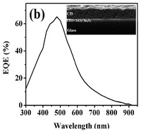
CuInS2 (CIS) thin films have proven to be promising candidates for photovoltaic technology but still the cost and safety of their fabrication processes remain challenging topics for research and development. Our efforts are based on avoiding the costly vacuum-based deposition methods that use selenization and high temperature processes. A cadmium free cell structure 〈glass/FTO/TiO2/In2S3/CIS/carbon〉 was fabricated using a CuInS2 nanocrystal ink at low temperature without selenization or sulfurization steps. All processes used have been non-vacuum and solution based. To form a stable ink, surfactant and binder-free monodispersed CIS nanocrystals were synthesized via a hot injection method in ethylene glycol solvent and re-dispersed in DMF. A spray pyrolysis method was used for the deposition of TiO2 and In2S3 as blocking and buffer layers, respectively. A doctor blade method was used to coat CIS films on the buffer layer. The final CIS absorber layer was achieved after heat treatments at 150 and 250 °C, without a selenization process. The amount of carbon residue in the final CIS film was very low (∼3%). Effective parameters on photovoltaic performance including the type of sulfur source, buffer-layer thickness and CIS grain size and morphology were optimized. The optimum superstrate-type solar cell device showed promising power efficiency of up to 3%.


1. Introduction

Among natural resources, solar energy provides a clean and low cost source of energy that has been widely employed to generate electrical power for public facilities. Nowadays, chalcogenides have attracted a great deal of attention as potential absorber candidates for thin layer technology.1–4 Within the chalcogenide family, CuInS2 (CIS) is predicted to be a promising choice as an absorber layer in thin film solar cells due to its high light absorption coefficient and direct band gap (1.5 eV) that is well matched with the visible region of the solar spectrum.5–9 Currently, the solar cell efficiency of 11.4% for CIS has been achieved via a vacuum based preparation technique.10 However, high efficiency polycrystalline thin-film CIS solar cells require the deposition of the absorber layer to be via vacuum deposition techniques such as evaporation and through the use of sulfur or selenium atmospheres at high temperature.11–14 In spite of the high efficiency and good crystallinity of products from vacuum-based methods, three factors have limited the development of CIS solar cells on a large scale: high production costs, waste material and the use of toxic elements (selenium).15–17 The key factor to develop power generation using CIS solar cells is to reduce the power generation cost. Nowadays, there is great interest in expanding low-cost processing methods to the growth of high-quality CIS-type absorbers for thin film solar cell applications. Over past years, many efforts have been focused toward non-vacuum deposition methods and using superstrate-type configurations for CIS solar cells; however, power conversion efficiency is very limited when using these techniques.17–21 Among the main categories of non-vacuum approaches for the deposition of inorganic absorber layers, solution based processes are among the techniques that offer great potential for simple fabrication methods and low cost photovoltaic device solar cells. This approach is based on the printing/coating of precursor solution ink22,23 or nanoparticle ink.24,25 The superiority of precursor ink is its simple preparation. But it has some obstacles: the ink is very unstable, and the use of organic binders to get suitable rheological properties for these ink coatings leads to incomplete decomposition of the organic content and carbon residue in the absorber film, resulting in shunt or recombination centres.26,27 Nanoparticle inks are prepared via the synthesis of CIS nanoparticles, followed by extraction, washing and re-dispersion in a suitable solvent. This technique allows purification of the ink through washing and extraction steps.28 On the other hand, the stability of nanoparticle ink is better than precursor ink. In general, the stability and homogeneity of the nanocrystal composition and size are two important parameters for preparation of a suitable ink. However, in many reports of nanoparticle ink, surfactants or stabilizers are used to control the composition or viscosity of the ink. But for high efficiency devices and low cost printing at large scale, removal of these surfactants or stabilizers is necessary.29,30

An investigation of high efficiency solution based processes shows that most reports are related to approaches that use hydrazine as solvent. However, hydrazine has several problems; this solvent is very toxic and hazardous. On the other hand, many metal precursors hardly dissolve in this solvent or are insoluble.31–33 Polyalcohol systems (like EG, DEG, TEG) are low cost and less toxic and metal precursors such as cupric salts and indium salts have much higher solubility in these systems, leading to greater yield.34,35 Here, we have used ethylene glycol (EG) and metal chlorides as a solvent and as metal precursors, respectively, for the surfactant- and binder-free synthesis of CIS via a hot injection route. We have also investigated the effect of sulfur source on the quality of the ink. The ink was formed by the extraction of nanoparticles and followed by redispersion in DMF. The final CIS ink was used as an absorber layer in a totally solution processed CIS solar cell with a superstrate-type configuration under atmospheric conditions. Our efforts are based on avoiding the costly vacuum-based deposition methods that use selenization and high temperature processes. The cadmium free cell structure 〈FTO/TiO2/In2S3/CIS/carbon〉 was fabricated at low temperature and without selenization or sulfurization steps. For optimizing the cell performance, the relationship between photovoltaic performance and the synthetic/geometric parameters (e.g. CIS annealing temperature, buffer-layer thickness, distance between the spray nozzle and film surface) were investigated. The resulting CIS thin films showed promising power conversion efficiencies of up to 3%.

2. Experimental section

2.1. Materials

Copper(I) chloride (CuCl, 99.99%) and indium(III) chloride (InCl3, 99.99%) were purchased from Sigma Aldrich. Thiourea (CH4N2S, 99.99%), thioacetamide (C2H5NS, 99.99%), ethylene glycol (C2H6O2), tetraisopropyl titanate, acetyl acetone, ethanol and N,N-dimethylformamide (DMF) were purchased from Merck. All chemicals were used without further purification.

2.2. Synthesis method

CuInS2 nanoparticles were synthesized via a hot injection technique. A typical synthesize procedure was performed under an atmosphere of argon in order to purge water and oxygen during the reaction. The experimental procedure was undertaken as follows: 0.9 mmol of copper(I) chloride (CuCl) and 1 mmol of indium(III) chloride (InCl3) were dissolved into 12 mL ethylene glycol in a 100 mL three-neck flask under an Ar atmosphere. Subsequently, they were mixed together for 45 min at 120 °C. At the same time 5 mmol of thiourea was separately dissolved in 6 mL of ethylene glycol under an argon atmosphere at 100 °C. The Cu/In/S ratio was adjusted to 0.9/1/5 to obtain Cu-poor and S-rich stoichiometry. After preparing two solutions, the thiourea solution was slowly injected into the first solution. After that, the temperature of the reaction mixture was quickly increased to 200 °C and the colour changed from sky-blue to colourless and finally to black. The black colour may be due to the formation of CuInS2 nanoparticles. The reaction mixture was refluxed under an argon flow for 60 min at 200 °C. Afterward, the solution mixture was cooled down to room temperature. The obtained colloidal solution was then centrifuged at 8300 rpm for 15 min, the upper layer liquid was decanted, and the isolated particles were washed with ethanol. Dispersion of the final nanoparticles in DMF formed a viscous and stable ink which can be easily deposited onto substrates. For further study, the sulfur source was altered from thiourea (TU) to thioacetamide (TAA) and thiosemicarbazide (TSC).

2.3. Device fabrication

The CIS solar cells were fabricated in a superstrate-type configuration 〈FTO/TiO2/In2S3/CIS/carbon〉. The FTO (15 Ω cm−2, Dyesol) was first put in a bath with soap and water. After that, it was cleaned prior to film deposition using ultrasonication for 15 min in HCl, ethanol and acetone solvents, and followed by heat cleaning at 500 °C. A TiO2 dense blocking film (∼100 nm) was deposited using a spray pyrolysis method at 450 °C from a solution containing ethanol, acetyl acetone and titanium tetraisopropoxide (TTIP) as previously reported.36 The spray solution was obtained by dissolving 0.72 mL TTIP and 0.108 mL acetyl acetone in 15 mL ethanol. An aluminium nozzle and sensor hot plate were used for the spray processes and controlling the temperature. The samples were placed on a hot plate in air by maintaining the surface temperature at around 450 °C. The surface temperature is critical and should be uniform over the sample. The other critical parameters for the spray method are the distance between the nozzle of the nebulizer and the sample, and the surface temperature of the sample. For the spray pyrolysis method, droplet size is an important factor. Spray over a large distance leads to non-uniform films with poor adhesion due to the formation of solid nanoparticles and precipitate on the hot surface, resulting in a nanoporous film. If the distance between the nozzle and the hot plate is small the droplets have not fully evaporated but will have precipitated, like rain drops, on the surface. The quality of the obtained layers is low, since the adhesion is poor and usually many pinholes are formed. The desired deposition regime lies between these two extremes.37,38 Noting the mentioned points, the desired distance between the nozzle of the nebulizer and the hot plate was 22 cm. Also, for setting the spray speed, we used an air compressor and the spray speed was adjusted to 1 mL min−1. After spray deposition, the films were kept at 450 °C for 60 min.

An In2S3 buffer layer was coated onto the surface of the TiO2 compact layer using the spray method. An aqueous solution of InCl3·4H2O and thiourea was used to deposit the In2S3 film on the TiO2 layer. These materials with a molar ratio (In[thin space (1/6-em)]:[thin space (1/6-em)]S) of 1[thin space (1/6-em)]:[thin space (1/6-em)]6 were slowly dissolved in 6 mL of distilled water. The concentration of the In2S3 precursor solution was 0.25 mol L−1. The spray process of the solution was carried out at a speed of 4 mL min−1 at 350 °C and the distance between the nozzle and film surface was maintained at 18 cm. Finally, the films were cooled to room temperature.

In the next step, the CIS nanocrystal films were deposited using a simple knife coating. Typically, a small amount of the concentrated CIS nanocrystal ink was dropped at one edge of the In2S3 buffer layer. A glass rod was then swept over the substrate to create a uniform coating. The as-deposited films were then placed on a preheated 150 °C hot plate for 10 min. Without cooling, the heated sample was immediately moved to a preheated 250 °C hot plate and maintained at this temperature for 10 min until the solvents and anions were removed by thermal evaporation and decomposed by air annealing, respectively. After heat treatment, the samples were allowed to cool to room temperature in an air environment. At the end, the thin film was covered by a layer of carbon polymer (Sharif Solar) as the back contact and then dried in an oven at 120 °C for 20 min. The total active area was 0.16 cm2. The JV measurements were operated under a simulated air mass 1.5 global illumination.

2.4. Characterization

The crystal structural properties were determined with X-ray diffraction (XRD) using a Philips X-pert X-ray diffractometer using Cu Kα radiation (wavelength, λ = 1.5418 Å). The SEM images of the films were taken using a Philips XL-300. Fourier transform infrared (FT-IR) spectra were determined on a Shimadzu-8400S spectrometer in the range of 400–4000 cm−1 using KBr pellets. Diffuse reflectance spectroscopy (DRS) was measured using a Shimadzu-UV-2550-8030 spectrophotometer. The optical properties of the deposited layers were determined by measuring the transmittance and absorbance spectra using the Shimadzu-UV-2550-8030 spectrophotometer in the range of 190–1000 nm. The performance of the solar cells were measured using a solar simulator (Sharif Solar) equipped with a source meter (Keithely 2400). The power of the simulated light was calibrated to AM 1.5 (100 mW cm−2) using a standard photo diode. The cells were characterized under a mask by covering the glass edges.

3. Results and discussion

3.1. CIS film characteristics

Improvement of the rheological properties and homogeneity of the nanocrystal composition and size is a basic parameter for preparing a suitable ink from the sulfide nanocrystal thin film deposition method. A huge barrier to the achievement of a suitable ink formulation is the use of various organic ligands, surfactants, or stabilizers, which are difficult to remove post-film coating. In this study, we tried to develop a surfactant and binder free synthesis method for the preparation of CIS nanoparticle inks. The prepared inks were then used in a cost effective coating method. Using a suitable solvent that has functional groups which can effectively stabilize nanocrystals and act as a capping agent is a critical factor for the preparation a nanocrystal ink. Accordingly, N,N-dimethylformamide (DMF) was chosen as a suitable candidate in this work because its functional groups can stabilize the nanocrystals effectively. We have used no binder, surfactant or stabilizer to prepare our nanocrystal ink because of the strong coordination effect of the DMF functional group. On the other hand, due to the moderate boiling temperature of DMF (150–154 °C), residual organic solvent in the final coated thin film can be easily removed by a mild heating treatment in air. After re-dispersing the CIS nanocrystals in DMF (200 mg mL−1), a viscous ink was obtained that could be applied directly on the In2S3 buffer layer.

3.2. Structural description of the product

The XRD pattern of the as-prepared CIS nanoparticles prepared via a hot injection method at 200 °C is shown in Fig. 1a, (I). The pattern indicates that the as-prepared product has a crystalline structure. All diffraction peaks can be indexed to the pure chalcopyrite phase of CuInS2 by comparison with data from JCPDS file no. 750106. Bragg reflections for the CIS NPs are observed in the XRD pattern at 2θ values of 27.97°, 46.43° and 55.16°, indicating the presence of chalcopyrite crystals. Based on the XRD results, there are no peaks of the other impurity phases such as CuS and In2S3. So the pure phase of chalcopyrite CIS has been achieved. Fig. 1a, (II) shows the XRD pattern of the CIS film deposited on soda lime after thermal treatment at 250 °C. The XRD pattern of the resulting product matches closely with the characteristic peaks of the chalcopyrite phase of CuInS2 (JCPDS no. 750106). The diffraction peaks at 2θ values of 27.97°, 32.40°, 46.43° 55.16°, 67.90° and 74.88° are assigned to the (120), (200), (204), (312), (400) and (316) planes of the chalcopyrite CIS phase. The XRD pattern revealed sharp peaks, indicating a high degree of crystallinity. Furthermore, no characteristic peaks related to impurities can be found in the XRD patterns, and as a result, the XRD data shows that only CIS phases exist in the films. The XRD pattern of the CIS film after a second annealing process at 250 °C shows stronger peak intensities compared to the as-prepared CIS nanoparticles, which indicates better crystallinity for the annealed film than the as prepared nanoparticles, resulting in an improvement of Jsc and the FF.
image file: c5ra17745f-f1.tif
Fig. 1 (a) XRD patterns of the as prepared CIS nanoparticles via a hot injection method at 200 °C (I) and annealed CIS film at 250 °C for 10 min (II). (b) XRD pattern of the In2S3 buffer layer. (c) XRD pattern of the TiO2 compact layer. (d) Typical EDS pattern of the CIS film after annealing at 250 °C.

A possible formation mechanism of nanocrystalline CuInS2 is proposed based on the experimental results. In this work, chloride salts of metals and thiourea were dissolved in ethylene glycol as the metal precursors and sulfur source, respectively. After dissolving metal precursors up to 100 °C, the formation of Cu–EG and In–EG complexes can be detected through changes in the solution colour that are shown in the proposed eqn (1) and (2). The solution colour was sky blue up to 100 °C due to the formation of a copper complex:39

 
CuCl + C2H6O2 → [Cu(EG)]+ (1)
 
InCl3 + C2H6O2 → [In(EG)]+ (2)

When the temperature exceeded 100 °C, the colour changed to dark bluish green. The solution colour changed to light green at 120 °C because of the formation of an indium complex. In the second flask, by dissolving thiourea the solution was transparent. Subsequently, by increasing the temperature above 150 °C, the Cu–EG and In–EG complexes decomposed to produce copper and indium ions and the solution changed to colorless. At this temperature, injection of the sulfur source into a copper and indium solution could result in the nucleation of a nanocrystalline solid along with their growth. At about 200 °C, smoke began to evolve and the colour turned from transparent to brown and finally to black which indicated complex decomposition followed by the nucleation of nanocrystals.

 
Cu+ + In3+ + S2− → CuInS2 (3)

The extra ethylene glycol and thiourea play the role of capping agents via the reaction of hydroxyl (OH) ligand with the nanoparticle surface.

Fig. 1b shows the X-ray diffraction pattern of the In2S3 buffer layer derived from a 6 mL spray of InCl3·4H2O and thiourea aqueous solution at 350 °C for 1.5 min. All the resultant products displayed the characteristic XRD peaks corresponding to the face-centered cubic structure of In2S3, according to JCPDS card no. 25-0390. No XRD peaks arising from possible impurities such as In2O3, InS, and other phases of In2S3 were visible, suggesting the formation of a pure cubic phase of In2S3.

Fig. 1c shows the XRD pattern of the TiO2 compact layer that was deposited by the spray pyrolysis method at 450 °C. The XRD peaks for TiO2 at 26.6°, 44.2°, and 52.3° are indexed to the (112), (220/204), and (321/116) reflections of the anatase structure, in which the observed peaks match well with the reference JCPD data (JCPDS card no. 21-1272).

Fig. 1d shows the typical EDAX pattern of the CuInS2 film after annealing at 250 °C. For each sample, EDAX was taken from different points on the surface and their mean values were reported as the actual composition. The ratio of Cu[thin space (1/6-em)]:[thin space (1/6-em)]In[thin space (1/6-em)]:[thin space (1/6-em)]S is close to 0.9[thin space (1/6-em)]:[thin space (1/6-em)]1[thin space (1/6-em)]:[thin space (1/6-em)]2, which is obviously inconsistent with the Cu-poor CIS. As can be seen, the percentage of carbon in final film is very low in comparison to previous reports.40–43 A large problem with coating/printing thin layers is the presence of carbon impurity in the final film that can cause shunt paths across the film. Therefore, charge recombination is enhanced and the open circuit voltage (Voc) of the solar cell device is diminished. On the other hand, removal of organic residues in the film due to thermal treatment may increase voids and cracks in the final film. Considering that the Cu[thin space (1/6-em)]:[thin space (1/6-em)]In[thin space (1/6-em)]:[thin space (1/6-em)]S precursor ratio was 0.9[thin space (1/6-em)]:[thin space (1/6-em)]1[thin space (1/6-em)]:[thin space (1/6-em)]5 in the starting materials, excess S in the precursor solution may have been lost during the sintering process in the air environment. Compared to the stoichiometric ratio, excess thiourea has been used to avoid the formation of a white precipitate related to a Cu–thiourea complex.44 On the other hand, we have used Cu-poor stoichiometry because it is an important parameter in controlling the chemical composition of final film in order to obtain highly efficient solar cells. The Cu-poor films have two advantages: (i) avoiding of the formation of highly conductive unfavourable impurity phases such as Cu2−xS, Cu3S2, and CuS, consequently removing the need for a toxic KCN post-treatment step, and (ii) improvement of the semiconducting properties, such as charge carrier mobility and carrier concentration.45,46

Fig. 2a shows the SEM image of the CIS sample prepared with thiourea as the sulfur source. The image shows a particle morphology that is typical of a low temperature approach. The nanoparticles are relatively uniform in size with an average particle size of 50 nm and a standard deviation of 3.2 nm. The histogram of the particle size distribution for the obtained product has been shown in Fig. 2a using a microstructure measurement program and Minitab statistical software. Fig. 2b shows a cross sectional SEM of the CIS film annealed at 250 °C for 10 min. There are no cracks in the as-deposited thin film during the drying procedure, and the layer is roughly 1.8 μm thick. It can be seen from Fig. 2b that heating the CIS film at 250 °C leads to a structure that has some voids, possibly resulting from the decomposition of volatile surface ligands and precursor materials. On the other hand, the particles fused together and created a well-connected network that is important for efficient carrier transport.47 Also, crystal growth due to thermal treatment is clearly observed. The size of the particles is up to 200 nm which is larger than previous work on low temperature device fabrication without a selenization step.17–19 Fig. 2c and d show the SEM images of spray deposited TiO2 and In2S3 films respectively. The packed film shows a uniform thickness with no pores or cracks. These layers were achieved by optimizing the precursor concentration, spray time and nozzle distance from the hot plate.


image file: c5ra17745f-f2.tif
Fig. 2 (a) SEM image of the CIS sample prepared with thiourea as the sulfur source with a statistical graph of the particle size distribution of CIS nanocrystals prepared under optimal conditions in the inset and (b) cross sectional SEM of the CIS film annealed at 250 °C for 10 min. (c) SEM image of the spray deposited TiO2 blocking layer. (d) SEM image of the spray deposited In2S3 buffer layer.

The FT-IR spectra of the final annealed film at 250 °C is clear evidence of the purity of the final CIS film. The characteristic vibrations at 3417 cm−1 (ν(OH)) proves the presence of moisture on the surface of the CIS film. There are no peaks in the range 4000–400 cm−1, which proves that the annealed CIS film doesn’t have IR-active impurities (Fig. 3a). The organic molecules were removed by washing with ethanol and through thermal treatment.


image file: c5ra17745f-f3.tif
Fig. 3 (a) FT-IR spectra of the as-prepared nanoparticles and CIS film annealed at 250 °C. (b) Raman spectrum of the CIS film after annealing at 250 °C for 10 min. (c) XPS survey spectrum analysis of the CIS film prepared from ink. The films were dried at 150 °C for 10 min and then annealed at 250 °C for 10 min.

Because the deposition of CIS was carried out under air conditions at low temperature, Raman analysis was used to reveal the presence of secondary phases such as metal chalcogenides including InxSy and CuxSy, which are not well distinguished in the XRD analysis. The Raman spectrum of the CIS film is shown in Fig. 3b. The dominating CIS Raman peaks detected at 290 cm−1 and 340 cm−1 are related to the A1 and B2 modes of the chalcopyrite ordering. The XRD and Raman analysis results indicate the purity of the final CIS absorber phase.

An XPS survey spectrum analysis of the CIS film prepared from nanoparticle ink is shown in Fig. 3c. The XPS data shows the following impurities on the top surface of the film: Cl = 1.5%, C = 5.5%, N = 0.4% and it shows Cu/In = 0.92. XPS is a surface analysis technique and the data is not necessarily applicable to the bulk. The XPS data also shows a slight amount of oxygen on the surface which is expected with our air annealing of the films.

3.3. Effect of sulfur source

The CIS nanoparticles were prepared by refluxing an ethylene glycol solution containing CuCl, InCl3 and several sulfur sources. The XRD patterns of obtained CuInS2 using thioacetamide and thiosemicarbazide as the sulfur sources are reported in Fig. 4. In terms of phase identification, all of the diffraction peaks matched well with the chalcopyrite phase pattern (JCPDS no. 750106). This confirms that the nature of the sulfur source did not influence the phase of the final product.
image file: c5ra17745f-f4.tif
Fig. 4 XRD patterns of the as prepared CIS nanoparticles using thioacetamide (a) and thiosemicarbazide (b) as the sulfur source.

In the case of thioacetamide, no diffraction lines of impurities were identified in the XRD pattern and the intensity of the peaks implies the relatively good crystalline nature of this product (Fig. 4a). But, when TSC was employed as a sulfur source, there are diffraction lines of impurity phases (Fig. 4b). A peak at 25.9° and 52.9° in the XRD pattern could be attributed to the formation of CuS (JCPDS card no. 06-0464).48 The synthesized samples with different sulfur sources have the same XRD pattern but an influence on peak width and, consequently, the crystallite size of CuInS2 nanoparticles was observed.

The intensities of the three main peaks of the (120), (204) and (312) planes suggest that the crystal sizes in the synthesized samples with various sulfur sources are different. The results show that the crystal growth of CIS with thiourea is higher (Fig. 1a) than thioacetamide and thiosemicarbazide as sulfur sources (Fig. 4a and b). The XRD results show that TSC may not be a proper sulfur source for the synthesis of CIS nanoparticles under the arranged conditions of hot injection. Many studies on ternary I–III–VI2 semiconductors show that the shape and the size of the final product depends on the reaction solvents or surfactants. In this work, it was interesting that the size of as-prepared CIS nanoparticles were strongly influenced by the type of sulfur source.

Fig. 5 shows the effect of sulfur source on the shape and particle size. It is clear that the sulfur source plays an effective role in controlling the size of products. Since the reactivity of different sulfide sources is not the same in the coordination reactions, synthesized CuInS2 particles using different sulfide sources vary in shape and size. As can be seen by using TSC as the sulfur source, the particles were agglomerated (Fig. 5a). TSC can release sulfide ions quickly.49 Therefore the sizes of the particles were small, and small particles were fused to each other and large particle sizes are obtained for this product. When TAA was used as the sulfur source the particle sizes were around 90 nm. In the case of TAA, sulfur can be released more slowly, and the rate of growth was greater than the rate of nucleation and large particles were achieved. However, the results suggested that by altering the sulfur source from TAA to TU, the synthesized nanoparticles are uniform and the average particle size decreases from 90 nm to 50 nm.


image file: c5ra17745f-f5.tif
Fig. 5 SEM image of the CIS sample prepared with thiosemicarbazide (a) and thioacetamide (b) as the sulfur source.

3.4. Photovoltaic parameters

The CIS layer was tested as an absorber layer in a thin film solar cell device with a superstrate 〈SLG/FTO/TiO2/In2S3/CIS (absorber layer)/back contact〉 structure. Carbon polymer was used as the back contact. For deposition of the CIS layer, we used nanocrystal CIS ink prepared from the redispersion of nanoparticles (synthesized by thiourea as the sulfur source and a reaction time of 60 min) in DMF.

The current density versus voltage (JV) characteristics were measured under 100 mW cm−2 illumination. Photovoltaic parameters such as Jsc (the short-circuit current), Voc (the open-circuit voltage) and FF (fill factor), which are significant factors that explain the performance of a solar cell device, were measured. For the optimum cell, the short-circuit current density, Jsc, was 15.52 mA cm−2, which is improved compared to previous reports for superstrate-type CIS solar cell devices.17–21 The power conversion efficiency, η, the fill factor (FF) and open-circuit voltage (Voc) were 3.03, 43% and 454 mV, respectively. The low open circuit voltage may be caused by recombination through the interface, the space charge region or the bulk of the absorber layer.40 Meanwhile, we believe that this might be due to film voids. Organic residue from precursor can be exited in the second annealing of the CIS film at 250 °C, resulting in the production of a structure that has some voids.

Fig. 6a shows the current–voltage diagrams of the cells fabricated by using different sulfur source based ink formulations. The results suggest that the type of sulfur source highly influences both the Jsc and Voc of the devices. By altering the sulfur source from TU to TAA, both the current density and open-circuit voltage are diminished. For TSC, the results were disappointing and the Jsc and Voc values were negligible (Table 1).


image file: c5ra17745f-f6.tif
Fig. 6 (a) Current–voltage diagrams of the cells fabricated using different sulfur source based ink formulations. (b) External quantum efficiency (EQE) of the optimum CIS solar cell. (c) Bandgap (Eg) determination of the device from the EQE data. (d) JV curves obtained from the device prepared at various annealing temperatures.
Table 1 The device performance parameters for CIS cells fabricated using nanocrystal inks based on different sulfur sources. Here, TU represents thiourea, TAA represents thioacetamide and TSC represents thiosemicarbazide
Sulfur source Buffer layer deposition Jsc (mA cm−2) Voc (mV) FF (%) Efficiency (%)
TU Spray 15.52 0.454 43 3.03
TAA Spray 8.67 364 42 1.36
TSC Spray 3.71 359 29 0.64


The final morphology of the CIS film is essentially the contribution of the sulfur source in the ink. For TU based inks, a rather dense and uniform layer is formed (Fig. 2), while this is not the case for TAA and TSC inks where the layers show voids and porosity (Fig. 5). Morphology plays a critical role in solution processed solar cells, by affecting defect density and recombination. All of the three sulfur sources operate as sulfur sources and also as capping agents to form the product. The number of NH2 functional groups connected to the C[double bond, length as m-dash]S agent in TAA is less than in TU and TSC. Therefore, the probable coordination manner of TAA to metal ions is restricted, while TSC and TU molecules have a strong tendency to coordinate with metal cations and easily form precursor complexes. The nucleation and growth play critical roles in the particle size of the final product. In the case of TAA, the release rate of sulfur was lower than TU and TSC, so the rate of growth was superior. Consequently, larger particles were obtained in comparison with TSC (Fig. 5). Since the TSC molecules which have more NH2 functional groups than TAA and TU can immediately release sulfur, the rate of nucleation will be greater than growth. Therefore the sizes of particles were small, and small particles fused together, and consequently a sponge shape morphology was attained for this sulfur source. When changing the sulfur source to thiourea, the rate of nucleation and growth was optimal and separated microspheres with small particles were achieved.

Fig. 6b shows the external quantum efficiency (EQE) response from a CIS superstrate solar cell fabricated using nanoparticle ink. Jsc was calculated by convoluting the EQE response using the following equation:

Jsc = ∫phEQE(λ),
where ϕph is the spectral photon flux density of the AM 1.5 spectral intensity distribution as a function of the incident light wavelength and q is the charge of the electron.50 The calculated Jsc value from the EQE spectra is 15.2 mA cm−2, close to the measured Jsc value (15.52 mA cm−2) obtained from the current density–voltage curve, as shown in Fig. 6a. The EQE shows a maximum of ≈67% at a wavelength of 480 nm and extends up to 920 nm with a gradual decrease. The EQE response decreases at higher wavelength and the appearance of a long tail at wavelength above 600 nm suggests that bulk recombination dominates in the absorber layer. This is related to the insufficient crystallinity of CIS films. This is partially due to the lack of high temperature sulfurization or selenization. The tail seen at wavelengths >700 nm is typically related to the presence of midgap states and shallow traps below the band edge.47

The bandgap determination of the CIS layer from the long-wavelength “absorption” edge of the EQE curve is shown in Fig. 6c. The band gap was determined to be 1.55 eV by fitting a plot of [E[thin space (1/6-em)]ln(1 − EQE)]2 against energy (E), which matches closely with the previous reported values for chalcopyrite CuInS2 thin films.51–53

3.4.1. Effect of annealing temperature. The effect of the second annealing temperature on the quality of the CIS film and device performance was investigated (Fig. 6d). Table 2 lists the photovoltaic parameters for different second annealing temperatures for the CIS film. The influence of annealing temperature was determined for samples with a TiO2 compact layer and an In2S3 buffer layer with 100 and 60 nm thickness, respectively.
Table 2 The device performance parameters for the cells, with the CIS film annealed at 200–300 °C. The optimum temperature lies between 200 °C and 300 °C
CIS crystallization temperature (°C) Jsc (mA cm−2) Voc (V) FF (%) Efficiency (%)
200 8.82 459 36 1.48
250 15.52 454 43 3.03
300 2.40 264 32 0.20


The best results were achieved from the CIS annealing temperature at 250 °C with an efficiency of 3.03%. An increase of annealing temperature leads to an increase in grain size (Fig. 7), resulting in photocurrent improvement. The improvement of photocurrent is related to the reduction in grain boundaries, which can significantly contribute to the formation of recombination centres. According to the data in Table 2, by increasing of annealing temperature from 200 to 250 °C, the photocurrent density is increased from 8.82 to 15.52 mA cm−2. On the other hand, the organic residues present in the as-prepared film were removed by the second annealing process. Consequently, the number of voids increased with increasing annealing temperature (Fig. 7). In the superstrate structure of the CIS solar cells, the filling of these voids with buffer during buffer layer deposition can help charge carrier separation through the creation of an interpenetrating heterojunction interface. However, in view of our cell configuration (carbon/CIS/In2S3/TiO2/FTO), the presence of pores allows carbon to penetrate in the CIS layer and form shunt paths through direct contact with the In2S3 buffer layer, which decreases cell performance.47 When the second annealing temperature was increased above 250 °C device operation was deteriorated and the cell showed weak performance.


image file: c5ra17745f-f7.tif
Fig. 7 Top-view SEM images showing the morphological changes on the surfaces of the CIS films prepared by the printing of CIS nanocrystal ink at (a) 200 °C (b) 250 °C and (c) 300 °C.
3.4.2. Effect of buffer layer thickness. N-type wide band gap materials such as: CdS, ZnS and In2S3 have been used as buffer layers in chalcogenide solar cells,17–21 and cadmium sulfide has been extensively used in high efficiency CIGS solar cells. But, we have avoided this material because of the presence of cadmium as a toxic and carcinogen element. We have used In2S3 as a buffer layer. In the view of our cell configuration (carbon/CIS/In2S3/TiO2/FTO), the buffer layer plays the following roles:

(I) Improvement of the junction properties between the absorber and window layers.

(II) Preventing the formation of recombination centers such as interface traps and defect states.

(III) Protection of the absorbing layer from mechanical and chemical damage.

(IV) Enhancing the thickness of the depletion layer.

Here, spray pyrolysis was used to deposit the TiO2/In2S3 layer. An In2S3 buffer layer was deposited to form a thin layer on a TiO2 packed layer and to form a p–n junction configuration using p-type CIS as an absorber layer. The results showed that the buffer layer thickness and quality has a critical role in the device performance. The performance parameters for the devices with different In2S3 thickness are summarized in Table 3. We did not observe considerable photovoltaic response in the absence of a buffer layer which means that electrons were not injected directly into the TiO2 blocking layer without the In2S3 buffer layer. The band gap of In2S3 is 2.1 eV (ref. 54) which is increased to 2.8 eV (ref. 55) for thin films of In2S3 with small grains contaminated with oxygen. The conduction bands of In2S3 and CuInS2 are close together and have an offset of about 1 eV compared to the conduction-band energy of anatase TiO2.56 Therefore, electrons of the conduction band can be easily injected into the conductive band of TiO2, which is located close to 4.2 eV,57 through the interface between CuInS2 and In2S3. Also, due to the 1 eV energy gap, back flow and return to the CuInS2 conduction band is impossible. On the other hand, TiO2 and CIS physically separate with the presence of a 60 nm thin In2S3 buffer layer. Consequently, the recombination of conduction-band electrons of TiO2 with valance-band electrons of CIS seems to be implausible. Therefore, in applying a buffer layer, both Jsc and Voc are improved.58

Table 3 The dependence of device performance on the deposition of the In2S3 buffer layer
Thickness of In2S3 layer (nm) Jsc (mA) Voc (mV) FF (%) Eff (%)
0 Device failure
30 4.65 245 30 0.33
60 15.52 454 43 3.03
90 9.6 494 46 2.19


The best device performance was achieved with an intermediate thickness (60 nm). This layer is packed and shows uniform thickness (Fig. 2c). Compared with the other device parameters, the open circuit voltage was changed with the altering of the thickness of buffer layer. The In2S3 layer improves the junction properties between the absorber and window layers and prevents the formation of recombination centers such as interface traps and defect states. Increasing the buffer layer thickness leads to an increase of depletion layer thickness (where photogenerated charges are separated under a strong electric field, extended along either side of the p-type and n-type semiconductors), resulting in decreasing interfacial recombination, enhancement of carrier density and better electron–hole separation. Consequently, the open circuit voltage was improved with a thicker In2S3 shell layer. On the other hand, the 60 nm thick buffer layer showed a high quality deposition (Fig. 2d). This layer provided a lower recombination probability during the efficient transfer of the generated charge carriers from CIS to In2S3/TiO2 (Fig. 8).


image file: c5ra17745f-f8.tif
Fig. 8 Illuminated JV curves obtained from the photovoltaic devices prepared using spray pyrolysis over In2S3 buffer layers with different thickness.

4. Conclusions

In summary, CIS nanocrystal ink was synthesized using a hot injection process using copper(I) chloride (CuCl), indium(III) chloride (InCl3) and several sulfur sources (TU, TAA and TSC) in ethylene glycol solvent. CIS nanocrystal ink was fabricated by extracting nanoparticles and re-dispersing them in DMF. The purity of the CIS layer was confirmed using FTIR, EDS and XRD analysis. In the final deposited film, the carbon content was negligible (about 3%). All solution-based CuInS2 superstrate-type solar cell devices were fabricated under atmospheric conditions and without selenization or sulfurization steps. Effective parameters of device performance such as the type of sulfur source, annealing temperature, and buffer layer thickness were investigated. Results showed the rate of sulfide ion release influences the morphology and particle size of the final product. Also, crystal growth and the number of voids in the final annealed film are related to the second annealing temperature and therefore cause considerable Cu diffusion into the In2S3 buffer layer at high annealing temperatures of 300 °C and higher, resulting in device failure. It was also found that the quality of the In2S3 buffer layer is critically important. It was also found that the open circuit voltage was increased with the enhancing of the thickness of the buffer layer because of decreasing interfacial recombination, enhancement of carrier density and better electron–hole separation. The cell showed that the optimum performance was achieved with a TU based ink and at a 250 °C annealing temperature and with a 60 nm thick buffer layer. The conventionally layered FTO/CuInS2/TiO2/In2S3/carbon PV devices showed promising power conversion efficiencies of up to ∼3%.

Acknowledgements

A. H. C acknowledges the financial support from the Tarbiat Modares University. Support from the Iranian Nanotechnology Council and Sharif Solar Company is acknowledged. The authors gratefully acknowledge the contribution of Dr Masoumeh Chamack.

Notes and references

  1. S. Seike, K. Shiosaki, M. Kuramoto, H. Komaki, K. Matsubara, H. Shibata, S. Ishizuka, A. Yamada and S. Niki, Sol. Energy Mater. Sol. Cells, 2011, 95, 254 CrossRef CAS.
  2. A. Virtuani, E. Lotter, M. Powalla, U. Raub, J. H. Werner and M. Acciarri, J. Appl. Phys., 2006, 99, 014906 CrossRef.
  3. P. O. Westin, U. Zimmermann, M. Ruth and M. Edoff, Sol. Energy Mater. Sol. Cells, 2011, 95, 1062 CrossRef CAS.
  4. J. Palm, V. Probst and F. H. Karg, Sol. Energy, 2004, 77, 757 CrossRef CAS.
  5. A. Cho, S. J. Ahn, J. H. Yun, J. Gwak, H. Song and K. Yoon, J. Mater. Chem., 2012, 22, 17893 RSC.
  6. G. Norsworthy, C. R. Leidholm, A. Halani, V. K. Kapur, R. Roe, B. M. Basol and R. Matson, Sol. Energy Mater. Sol. Cells, 2000, 60, 127 CrossRef CAS.
  7. X. Lu, Z. Zhuang, Q. Peng and Y. Li, CrystEngComm, 2011, 13, 4039 RSC.
  8. O. Kijatkina, M. Krunks, A. Mere, B. Mahrov and L. Dloczik, Thin Solid Films, 2003, 431–432, 105 CrossRef CAS.
  9. B. D. Weil, S. T. Connor and Y. Cui, J. Am. Chem. Soc., 2010, 132, 6642 CrossRef CAS PubMed.
  10. S. Siebentritt, Thin Solid Films, 2002, 1, 403–404 Search PubMed.
  11. G. M. Ford, Q. Guo, R. Agrawal and H. W. Hillhouse, Thin Solid Films, 2011, 520, 523 CrossRef CAS.
  12. Q. Guo, S. J. Kim, M. Kar, W. N. Shafarman, R. W. Birkmire, R. Agrawal and H. W. Hillhouse, Nano Lett., 2008, 8, 9 Search PubMed.
  13. S. H. Chang, M. Y. Chiang, C. C. Chiang, F. W. Yuan, C. Y. Chen, B. C. Chiu, T. L. Kao, C. H. Laic and H. Y. Tuan, Energy Environ. Sci., 2011, 4, 4929 CAS.
  14. Q. Guo, G. M. Ford, R. Agrawal and H. W. Hillhouse, Progress in Photovoltaics: Research and Applications, 2012, 64–71 Search PubMed.
  15. F. Long, W. M. Wang, H. Tao, T. K. Jia, X. M. Li, Z. Zou and Z. Fu, Mater. Lett., 2010, 64, 195 CrossRef CAS.
  16. D. C. Nguyen, K. Takehara, T. Ryo and S. Ito, Energy Procedia, 2011, 10, 49 CrossRef CAS.
  17. J. W. Cho, S. J. Park, W. Kim and B. K. Min, Nanotechnology, 2012, 23, 26540 Search PubMed.
  18. T. Ryo, D. C. Nguyen, M. Nakagiri, N. Toyoda, H. Matsuyoshi and S. Ito, Thin Solid Films, 2011, 519, 7184 CrossRef CAS.
  19. M. R. Balboul, A. Jasenek, O. Chernykh, U. Rau and H. W. Schock, Thin Solid Films, 2001, 387, 74 CrossRef CAS.
  20. L. Li, N. Coates and D. Moses, J. Am. Chem. Soc., 2010, 132, 22 CrossRef CAS PubMed.
  21. M. G. Panthani, V. Akhavan, B. Goodfellow, J. P. Schmidtke, L. Dunn, A. Dodabalapur, P. F. Barbara and B. A. Korge, J. Am. Chem. Soc., 2008, 130, 16770 CrossRef CAS PubMed.
  22. A. Cho, S. Ahn, J. Yun, J. Gwak, S. K. Ahn, K. Shin, H. Song and K. H. Yoon, Sol. Energy Mater. Sol. Cells, 2013, 109, 17 CrossRef CAS.
  23. S. Ahn, T. H. Son, A. Cho, J. Gwak, J. H. Yun, K. Shin, S. K. Ahn, S. H. Park and K. Yoon, ChemSusChem, 2012, 5, 1773 CrossRef CAS PubMed.
  24. Q. Guo, G. M. Ford, R. Agrawal and H. W. Hillhouse, Progress in Photovoltaics: Research and Applications, 2013, 21, 64 CrossRef CAS.
  25. H. T. Tung, I. G. Chen, J. M. Song, M. G. Tsai, I. M. Kempson, G. Margaritondo and Y. Hwu, Nanoscale, 2013, 5, 4706 RSC.
  26. Y. S. Lim, J. Jeong, J. Y. Kim, M. J. Ko, H. Kim, B. Kim, U. Jeong and D.-K. Lee, J. Phys. Chem. C, 2013, 117, 11930 CAS.
  27. S. J. Ahn, C. W. Kim, J. H. Yun, J. H. Gwak, S. H. Jeong, B. H. Ryu and K. H. Yoon, J. Phys. Chem. C, 2010, 114, 8108 CAS.
  28. A. Cho, S. Ahn, J. H. Yun, J. Gwak, H. Song and K. Yoon, J. Mater. Chem., 2012, 22, 17893 RSC.
  29. K. Ramasamy, M. A. Malik, N. Revaprasadu and P. O’Brien, Chem. Mater., 2013, 18, 3551 CrossRef.
  30. U. V. Ghorpade, M. P. Suryawanshi, S. W. Shin, C. W. Hong, I. Kim, J. H. Moon, J. Ho Yun, J. H. Kim and S. S. Kolekar, Phys. Chem. Chem. Phys., 2015, 17, 19777 RSC.
  31. D. B. Mitzi, Adv. Mater., 2009, 21, 3141 CrossRef CAS.
  32. T. Todorov and D. B. Mitzi, Eur. J. Inorg. Chem., 2010, 17 CrossRef CAS.
  33. D. B. Mitzi, M. Yuan, W. Liu, A. J. Kellock, S. J. Chey, L. Gignac and A. G. Schrott, Thin Solid Films, 2009, 517, 2158 CrossRef CAS.
  34. X. Sheng, L. Wang and D. Yang, J. Sol-Gel Sci. Technol., 2012, 62, 87 CrossRef CAS.
  35. H. Liu, Z. Jin, W. Wang, Y. Wang and H. Du, Mater. Lett., 2012, 81, 173 CrossRef CAS.
  36. M. Nanu, J. Schoonman and A. Goossens, Adv. Funct. Mater., 2005, 15, 95 CrossRef CAS.
  37. M. Krunksa, O. Kijatkina, H. Rebane, I. Oja, V. Mikli and A. Mere, Thin Solid Films, 2002, 403–404, 71 CrossRef.
  38. L. P. Deshmukh, R. V. Suryawanshi, E. U. Masumdar and M. Sharon, Sol. Energy, 2012, 86, 1910 CrossRef CAS.
  39. P. ShengJie, L. Y. Liang, C. F. Yi and L. I. Jing, Sci. China: Chem., 2012, 55, 1236 CrossRef.
  40. D. Lee and K. Yong, J. Phys. Chem. C, 2014, 118, 7788 CAS.
  41. C. Kind, C. Feldmann, A. Quintilla and E. Ahlswede, Chem. Mater., 2011, 23, 5269 CrossRef CAS.
  42. S. Ahn, T. H. Son, A. Cho and K. H. Yoon, ChemSusChem, 2012, 5, 1773 CrossRef CAS PubMed.
  43. U. Berner and M. Widenmeyer, Progress in Photovoltaics: Research and Applications, 2014, 1260–1266 Search PubMed.
  44. J. C. W. Ho, T. Zhang, K. Lee, S. K. Batabyal and A. I. Y. Tok, ACS Appl. Mater. Interfaces, 2014, 6, 6638 CAS.
  45. P. Niyamakom, A. Quintilla, K. Köhler, M. Cemernjak, E. Ahlswede and S. Roggan, J. Mater. Chem. A, 2015, 3, 4470 CAS.
  46. W. Septina, M. Kurihara, S. Ikeda, Y. Nakajima, T. Hirano, Y. Kawasaki, T. Harada and M. Matsumura, ACS Appl. Mater. Interfaces, 2015, 12, 6472 Search PubMed.
  47. H. Azimi, T. Heumüller, A. Gerl, G. Matt, P. Kubis, M. Distaso, R. Ahmad, T. Akdas, M. Richter, W. Peukert and C. J. Brabec, Adv. Energy Mater, 2013, 3, 1589 CrossRef CAS.
  48. Y. Li, J. Scott, Y. Chen, L. Guo, M. Zhao, X. Wang and W. Lu, Mater. Chem. Phys., 2015, 162, 671 CrossRef CAS PubMed.
  49. O. Amiri, M. Salavati-Niasari, M. Sabet and D. Ghanbari, Mater. Sci. Semicond. Process., 2013, 16, 1458 CrossRef.
  50. S. Merdes, R. SaezAraoz, A. Ennaoui, J. Klaer and R. Klenk, Appl. Phys. Lett., 2009, 95, 213502 CrossRef.
  51. H. Fakhri, A. R. Mahjoub and A. H. Cheshme Khavar, Appl. Sur. Sci., 2014, 318, 65 CrossRef CAS.
  52. B. Tell, J. L. Shay and H. M. Kasper, Phys. Rev. B: Solid State, 1971, 4, 2463 CrossRef.
  53. H. W. Schock, Sol. Energy Mater. Sol. Cells, 1994, 34, 19 CrossRef CAS.
  54. W. Rehwald and G. Harbeke, J. Phys. Chem. Solids, 1965, 26, 1309 CrossRef CAS.
  55. N. Barreau, J. C. Berende, X. Castel and J. Pinel, Solid State Commun., 2002, 122, 445 CrossRef CAS.
  56. S. Siebentritt, Thin Solid Films, 2002, 403–404, 1 CrossRef CAS.
  57. M. Gratzel, Nature, 2001, 414, 338 CrossRef CAS PubMed.
  58. M. Nanu, J. Schoonman and A. Goossens, Adv.Mater., 2004, 16, 453 CrossRef CAS.

This journal is © The Royal Society of Chemistry 2015