DOI:
10.1039/C5RA17228D
(Paper)
RSC Adv., 2015,
5, 78534-78544
Influence of silver grain size, roughness, and profile on the extraordinary fluorescence enhancement capabilities of grating coupled surface plasmon resonance†
Received
25th August 2015
, Accepted 8th September 2015
First published on 9th September 2015
Abstract
Since the development of fluoroimmunoassays, researchers have sought a method of substantially enhancing fluorescence intensity to extend the limits of detection to new levels of sensitivity. Surface plasmon resonance (SPR) and metal enhanced fluorescence has long been a topic of research and has led to the development of prism- and grating-based SPR systems. However, with the wide coupling range and ease of exciting SPR on plasmonic gratings with a simple microscope objective, they have tremendous potential for revolutionizing the fields of plasmonics, fluorescence, and sensors. In an effort to better understand the influence of grating profile and metal film properties on the extraordinary fluorescence enhancement capabilities of plasmonic gratings, a novel microcontact printing process and different metal deposition techniques were used to fabricate silver gratings with varying grain diameters, roughnesses, heights, and duty cycles using thermal evaporation and RF sputtering. The resulting plasmonic gratings exhibited fluorescence enhancements up to 116× that of dye-coated glass slides using an epifluorescence microscope, much higher than more expensive prism-based SPR systems. This silver grating represents an extraordinary opportunity to quickly and easily enhance fluorescence and widen the detection limits of common fluorescence based assays with little to no equipment modification.
Introduction
Surface Plasmon Resonance (SPR) research has grown substantially over the past several years and led to many substantial discoveries in nanotechnology including plasmonic nanoantennas and nanoresolution imaging techniques.1–6 SPR is essentially a phenomenon where light can be coupled into a metal/dielectric interface to form a propagating charge oscillation called a surface plasmon polariton (SPP). This method of light coupling only occurs if the wave vector of the incident light matches the wave vector of a SPP. Unfortunately, this does not occur under natural situations, which has led to the development of elaborate systems to form matching conditions that utilize structures such as nanoscale gratings, such as Fig. 1a.7–9 The expense of manufacturing platforms such as nanoscale gratings is currently cost prohibitive as it commonly involves the use of electron beam or interference lithography techniques.10,11 To reduce the cost of fabricating nanogratings, a novel soft lithography process was developed that can accurately replicate the gratings found on commercially available HD DVDs in polymethylsilsesquioxane (PMSSQ).12 To form SPR, a plasmonic metal coating, such as gold or silver, is required. While gold is typically chosen over silver due to its corrosion resistance, silver can support much higher field strengths due its inherently lower dielectric losses at optical frequencies.13 Using Maxwell's equations, a wave vector matching equation can be derived for a particular metal grating/dielectric interface, seen in eqn (1).12| |
 | (1) |
where ω is the frequency of the incident light, c is the speed of light in vacuum, εm is the dielectric constant for the metal, εd is the dielectric constant for the medium surrounding the metal, Λ is the grating pitch, kSPP is the wave vector of the surface plasmon, and m is an integer representing the diffraction order. In grating based systems, the diffraction of incident light results in an additional momentum term in the wave vector matching conditions. The range of values at which proper coupling conditions occur can be visualized in a frequency vs. momentum plots, seen theoretically in Fig. 1b and experimentally in Fig. 1c.13 Due to this shift in the surface plasmon momentum curve from grating diffraction, multiple frequencies can be used to form SPR at a single angle of incidence. An example of which are the two intersection points with the light line seen in Fig. 1b and c that correspond to the m = ±1 SPR modes.16 Furthermore, it can be observed that these two modes converge as the angle of incidence of light approaches θ = 0°. The ability to excite SPR at a low illumination angle on gratings has led to the development of systems that, for example, use microscope objectives to excite SPR instead of single angle, laser based systems.
 |
| | Fig. 1 (a) Illustration of the wave vector matching between incident EM radiation (transverse-magnetic (TM) light) on a grating and a propagating surface plasmon polariton. (b) Theoretical frequency vs. momentum plot for a metallic grating (red and black), and incident EM radiation (blue line).14,15 (c) Experimental frequency vs. momentum for a silver grating in air based on the SPR peak location from the reflectivity scans in Fig. 5. | |
As a better understanding of SPR has been obtained, a unique interaction was observed between the evanescent electromagnetic (EM) field formed during SPR and nearby fluorescent molecules. It was observed that the emission intensity of fluorophores could be drastically enhanced when located between 10 and 100 nm to the metal surface and a phenomenon later called metal enhanced fluorescence.17 If the frequency of the surface charge oscillation matched the excitation frequency of the fluorophore, the fluorophore would be excited to a higher energy state. However, due to the proximity to metal surface, the fluorophore would non-radiatively transfer energy to the metal and form a radiative plasmon with directed photon emission, also known as surface plasmon coupled emission (SPCE).18 To maximize fluorescent enhancement of this process, the EM field strength, which is closely tied to the properties of the metal/dielectric layers, must be tuned to be strong in the intended fluorophore excitation spectrum. Grating profile features such as height, pitch, and duty cycle as well as defects in the metal such as large grain boundaries and high roughness can have a strong effect on efficiency on SPR generation and must be further studied.
The objective of this study was to examine the effect of grating structure and silver film properties on SPR generation and fluorescence enhancement. Silver gratings with varying metal film and structural properties were fabricated using the previously mentioned microcontact stamping process. The surface structure, extent of light coupling, and fluorescence enhancement capabilities of the different silver gratings was then characterized with atomic force microscopy (AFM), variable angle spectroscopic ellipsometry (VASE), and fluorescence microscopy. To better understand the effect of surface structure on electric field strength, the grating structures were also reproduced in finite difference time domain (FDTD) simulations using FullWave software.
Results and discussion
Silver grating fabrication
HD DVD gratings (height: 60 nm, Λ: 400 nm) were replicated in polymethylsilsesquioxane (PMSSQ) “ink” with an added crosslinker, 3-aminopropyltriethoxysilane (APTES), using a previously developed microcontact stamping process depicted in Fig. 2 and further described in the Experimental section.12 As the gratings were fabricated using the fixed patterns of the HD-DVD, the capability to change the height, pitch and duty cycle of the polymer layer (PMSSQ) was limited. To study the effect of various parameters discussed above on light coupling and concentration, our novel approach was to control the surface energy of the polymer layer, deposition method (RF sputtering vs. thermal evaporation), and the use of different adhesion layers (chromium (Cr) for thermal evaporation, germanium (Ge) or titanium (Ti) for sputtering). The nucleation and growth of thin films relies on the energy of the incoming atoms and their adsorption, diffusion, coalescence/chemical binding to the surface.19 This was controlled by varying the energy of the incoming atoms, surface energy of the polymer film, and binding energy of Ge, Ti, and Cr (adhesion layer) to the polymer surface with and without plasma treatment, as well as, binding energy of Ag–Ag vs. Ag–Ti, Ag–Ge and Ag–Cr. While varying these parameters, it is important to pay attention to the grain size which should not be too large to increase the scattering losses, but small enough to concentrate SPR field (less than 50 nm). The surface energy of as prepared PMSSQ polymer layer was low (0.024 J m−2) due to inherent hydrophobicity of the film. Oxygen plasma treatment changes the film to hydrophilic with high surface energy (0.056 J m−2). The hydrophobic and hydrophilic nature of PMMSQ or wettability of the film is then used to control the interaction of the incoming atoms of the seed layers with PMMSQ surface and growth of the adhesion layer. Subsequently, silver atoms will interact with the seed layer and control the growth of silver films. Metal film growth in general can be described by three growth modes, the Frank–van der Merve growth seen in Fig. 3a (layer by layer growth), Volmer–Weber growth seen in Fig. 3b (island growth), and Stranski–Krastanov growth seen in Fig. 3c (layer and island growth).20 The deposition parameters and surface energy of PMMSQ were varied to control the nucleation and growth processes to achieve films with different silver grain sizes and are discussed in further depth below.
 |
| | Fig. 2 Soft lithography process diagram. (1) Cut and remove the PDMS stamp pieces from the disc mold; (2) spin coat PMSSQ “ink” solution onto the PDMS stamp; (3) stamp and peel off the PDMS onto a glass slide or silicon wafer. | |
 |
| | Fig. 3 Grain and island growth mechanisms for silver films deposited onto (a) germanium, (b) titanium, and (c) chromium adhesion layers. | |
Surface energy of PMMSQ films. Plasma treatment of PMSSQ creates a high surface energy surface by forming defects (dangling bonds) and surface bound –OH chemical groups. These sites can act as binding and nucleation sites that reduce the mobility of the adatoms and promote island grow, resulting in the formation of large metal grains. In the case of PMSSQ films without plasma treatment with low surface energy and low number of defect/binding sites, incident atoms can more readily diffuse to the surface, leading to coalescence, the formation of many new nucleation sites, and ultimately denser, smoother films.
Sputtering vs. thermal evaporation. The energy of the incoming atoms in a sputter deposition system range from 1–10 eV, whereas, for thermal evaporation, the incoming atoms have much lower energy that ranges from 0.1–1 eV.21 Due to the low energy of atoms in thermal evaporation, these atoms are less mobile and hence promote island and columnar growth resulting in the formation of large grains. Also, when the low energy atoms with directional flux are deposited in thermal evaporation onto a grating surface with nanoscale features (60 nm height and 400 nm pitch), the atoms tend to fill the groves and reduce the observed height of the gratings (see Table 1). In sputter deposition, the high energy and mobility of incoming atoms promotes layer by layer growth, as seen in Fig. 3a, resulting in smaller grains and smoother films with less groove filling.
Table 1 Summary of grating dimensions, roughness, and grain diameter
| Surface pre-treatment |
Deposition type |
Mean grating pitch, Λ [nm] |
Mean grating height [nm] |
RMS roughness [nm] |
Mean grain diameter [nm] |
Duty cycle |
| No |
Sputtered Ge/Ag |
401.4 ± 3.1 |
52.8 ± 1.9 |
1.6 |
31.7 ± 8.2 |
0.533 ± 0.018 |
| Oxygen plasma |
Sputtered Ge/Ag |
400.2 ± 3.5 |
55.7 ± 1.7 |
1.7 |
35.6 ± 9.1 |
0.552 ± 0.022 |
| No |
Sputtered Ti/Ag |
401.8 ± 3.4 |
53.1 ± 0.5 |
1.9 |
33.2 ± 9.3 |
0.512 ± 0.016 |
| Oxygen plasma |
Sputtered Ti/Ag |
396.7 ± 3.7 |
54.8 ± 1.6 |
2.5 |
39.0 ± 9.9 |
0.521 ± 0.018 |
| No |
Therm. evap. Cr/Ag |
403.3 ± 5.1 |
43.9 ± 1.9 |
4.0 |
40.1 ± 15.7 |
0.568 ± 0.027 |
| Oxygen plasma |
Therm. evap. Cr/Ag |
397.3 ± 8.2 |
42.9 ± 3.5 |
5.1 |
55.8 ± 17.5 |
0.569 ± 0.046 |
Effect of adhesion layer on silver film growth. Both of the two different adhesion layers, titanium and germanium, deposited by sputtering promote layer by layer growth on PMSSQ. However, when silver is deposited on germanium, the higher dissociation energy of Ag–Ge (174.5 kJ mol−1) compared to Ag–Ag (162.9 kJ mol−1) allows for smoother films with smaller grains than silver deposited on titanium.22,23 The Ti–Ti bond dissociation energy (117.6 kJ mol−1)22 is much lower than Ag–Ag, however, the much higher inherent energy of sputtered adatoms vs. thermal evaporation mentioned previously aids in diminishing the effect of the energy mismatch. It is speculated that this is the reason why the RMS roughness of such films are always slightly higher than silver films sputtered onto germanium. By obtaining relatively smooth films despite the great mismatch in dissociation energy between Ti and Ag, we also believe that the growth method is closest described by Volmer–Weber growth.24 In thermal evaporation, Stranski–Krastanov growth is favoured for an Ag film deposited onto an adhesion layer of lower dissociation energy, such as Cr–Cr (152.0 kJ mol−1),22 and the substantially lower adatom energy of thermally evaporated silver vs. RF sputtering.
Surface and optical characterization
Surface structure and permittivity. Grating surface structure was characterized with AFM and analysed using Gwyddion to obtain the pitch, height, root mean square (RMS) roughness, duty cycle, and grain diameter tabulated in Table 1 and shown in Fig. 4a–f. Grain diameter distributions were provided in Fig. 4g. 2D/3D projections of the AFM scans as well as grain diameter histograms for every sample with fitted Gaussian profiles have also been provided in Fig. S1.† All thermally evaporated samples exhibited larger diameters and wider dispersity than sputtered samples, which is consistent with the previously discussed grain growth mechanisms. Thermally evaporated sample grains also exhibited sharper edges than sputter samples. All plasma treated samples also exhibited increased grain diameters compared to non-treated samples due to the higher surface energy. The effect of the varying deposition techniques on the electric properties of the films was studied by comparing the complex permittivity obtained via spectroscopic ellipsometry for all of the silver films as seen in Fig. 4h and i. Little change in the real component of permittivity was observed between samples; however, the imaginary component associated with energy loss was substantially lower for thermally evaporated samples than sputtered samples.
 |
| | Fig. 4 Topographical AFM scans (1.5 μm × 1.5 μm) of gratings with (a and b) sputtered germanium and silver, (c and d) sputtered titanium and silver, and (e and f) thermally evaporated chromium and silver. Oxygen plasma treated samples (b, d and f) on average exhibited larger average grain diameters than the (a, c and e) untreated counterparts. All scan heights have been plotted from 0 to 60 nm. (g) Grain diameter histograms from the previous AFM scans. (h) Real and (i) imaginary permittivity components taken from flat silver films with the same deposition parameters and PMSSQ/APTES film surface energy with bulk silver values from Johnson and Christy.25 | |
Reflectivity. The formation of SPR on a metallic grating is commonly seen as a sharp dip in the reflectivity at particular wavelengths and angles of incidence.12,26 The depth of the reflectivity dip, also called the coupling strength (σ), is an indicator for how strongly light is coupled to the grating while full width at half maximum (FWHM) indicates the range of wavelengths that can couple at a particular angle of incidence. The reflectivity of the different grating samples has been plotted in Fig. 5a–f and Table S1.† Two sharp decreases in reflectivity for each angle of incidence correspond to the m = ±1 SPR solutions that are supported on the grating.6 For reference, the m = +1 SPR coupling wavelength has been indicated for all reflectivity curves in Fig. 5a–f at θ = 15° and θ = 45°. From the θ = 15° reflectivity of the six grating samples seen in Fig. 5g and Table S1,† a trend of increasing coupling strength with grain size can be observed. SPR coupling location found in reflectivity was plotted vs. angle of incidence to obtain a dispersion plot for several angles of incidence and can be seen in Fig. 5h. As angle of incidence approaches 0°, the SPR coupling wavelengths corresponding to the m = ±1 solutions converge as seen experimentally in Fig. 5h and 1b and c. Only minor variations in peak location were observed between sputtered and thermally evaporated samples which is largely attributed to similarity in grating pitch between samples.
 |
| | Fig. 5 TM-polarized reflectivity plots for 15° and 45° angles of incidence of gratings with (a and b) sputtered germanium and silver, (c and d) sputtered titanium and silver, and (e and f) thermally evaporated chromium and silver. Oxygen plasma treated (b, d and f) and untreated counterparts (a, c and e). (g) TM-polarized reflectivity at 15° of silver gratings with plasma, P, and no plasma treatment, NP. (h) Dispersion plot of the m = ±1 SPR modes derived from reflectivity peak location of silver gratings in air. | |
Fluorescent dye enhancement
Angled excitation. Single angle, monochromatic illumination is the most common form of SPR excitation found in literature. While this may be optimal for prism based-systems with narrow coupling ranges, it is much less effective for systems with wider coupling ranges, such as nanogratings. By exciting SPR on wide coupling range systems with a single wavelength and angle, a large portion of the SPR coupling range is underutilized. In order to take full advantage of the wide coupling range, the nanograting must be illuminated with polychromatic light that matches the excitation spectrum of the desired fluorophore at a range of angles that can couple to form SPR. This form of illumination can already be found in the objective of a simple fluorescence microscope as objectives focus light into a cone with a particular convergence angle as seen in Fig. 6a. The convergence angle of a particular objective can be calculated with eqn (2):| |
NA = n![[thin space (1/6-em)]](https://www.rsc.org/images/entities/char_2009.gif) sin(±θ) sin(±θ)
| (2) |
where ±θ is the maximum convergence angle of the objective from sample normal, NA is the numerical aperture, and n is the refractive index of the imaging medium. Using eqn (2), the convergence angles were calculated for the three objectives: θ10× = ±17.45°, θ20× = ±26.74°, and θ40× = ±36.87°. The angular illumination intensity of an objective is normally distributed with most of the light impacting the sample near 0° and only a small fraction of photons illuminating the sample at the convergence angle.27
 |
| | Fig. 6 (a) Illustration of SPR excitation and SPCE capture from a silver grating with a simple microscope objective. (b) SPR dispersion curve representing SPR coupling peak location with overlay of R6G excitation and emission spectrum. (c) Normalized objective illumination intensity vs. angle for 10×, 20×, and 40× objectives with estimated SPR excitation and SPCE emission angle ranges from (b) for a silver grating coated in 35 nm PMSSQ. (d) Mean enhancement factor of R6G dye coated gratings with different grain sizes as compared to R6G-coated glass substrates using 20 ms CCD exposure. | |
Dye selection. To obtain the highest fluorescent enhancement using gratings and a microscope objective, the selected fluorophore must have an excitation spectrum that overlaps with the low angle coupling range (θSPR = <10°) of the grating. To accurately determine the SPR dispersion of a dye-layer coated grating, a 35 nm thick PMSSQ layer was spin-coated onto the gratings, the addition of which will red-shift the SPR dispersion due to the higher refractive index of the PMSSQ compared to air. Reflectivity measurements were acquired on the PMSSQ coated grating without the fluorescent dye and the corresponding SPR dispersion has been provided in Fig. 6b. Using this dispersion, the optimal fluorophore must be excited near 530 nm and emit near 550 nm. Rhodamine 6G (R6G) was selected to test the enhancement capabilities of the grating due to its overlap with the low angle SPR dispersion and high photostability.
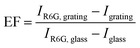
Fluorescence microscopy. As mentioned in the introduction, fluorophores can non-radiatively transfer energy to metal if the fluorophore is in close enough proximity to the metal surface. The spacing between the fluorophore and metal determines if the charge oscillation formed on the metal as a result of the energy transfer will be a lossy surface plasmon or a radiative plasmon.17 If very close (<10 nm), the charge spacing is too small to form a radiative plasmon resulting in the formation of a lossy surface plasmon. However, if the fluorophore is located between 10 and 100 nm from the surface, a radiative plasmon will form and directionally emit a photon via SPCE. The SPCE wavelength corresponds to the fluorophore emission wavelength and is emitted at the SPR angle. Using the SPR dispersion curve in Fig. 6b, the emission angle of R6G dye is estimated to occur between 3.6° and 8°. For an objective to capture SPCE, estimated to emit from the grating from 10° to 17°, the emission angle must fall within the convergence angle of the objective. The SPR coupling and SPCE emission spectrum of R6G was overlaid with the angular illumination intensity of the 10×, 20×, and 40× objectives in Fig. 6c. It can clearly be seen that the 10× objective provides the highest intensity excitation in the SPR coupling region while still encompassing the angular range of SPCE. It was calculated that the 20× and 40× objectives excite the grating with 84% and 47%, respectively, of the illumination area provided by the 10× intensity. It was also calculated that 32.4% of the 10× illumination cone is within the SPR excitation angle range while only 28.2% and 24.4% of the 20× and 40× illumination cones, respectively, is within the SPR coupling range. Dye-coated gratings and glass samples were imaged with all with all three objectives at an exposure time of 20 milliseconds and processed in ImageJ to obtain the raw fluorescence intensity. Example fluorescence images from the 10× objective have been provided in ESI in Fig. S2.† Fluorescence enhancement factor (EF) of the gratings was calculated using eqn (3).| |
 | (3) |
where I represents the intensity reported by the CCD with and without R6G on gratings or glass substrates. The resulting fluorescence enhancement of the gratings in different microscope objectives compared to dye-coated glass samples has been provided in Fig. 6d. The enhancement factors corresponded well with the estimated objective excitation area for each of the objectives with the 10× objective providing the highest enhancement overall as was expected. The evaporated silver sample with a 55.8 nm mean grain diameter exhibited the highest mean enhancement factor of 116× while the sputtered germanium–silver sample exhibited a mean enhancement factor of 55× compared with dye-coated glass. The high fluorescence enhancement found on these plasmonic gratings is attributed to the combination of using low loss silver films, optimized grating profiles, and a wide angle excitation source.These fluorescence enhancements are also higher than previously observed values for similar fluorescent dyes on plasmonic grating systems. Table 2 has been provided to summarize several recent fluorescence enhancement results on silver and gold gratings with varied parameters. The lower fluorescent enhancement seen in previous studies is thought to arise from the small grain sizes obtained through sputter coating, exciting the platform at a narrow angle range or too far away from the optimal objective illumination range, and incorporation of overly thick capping layers between the silver and the fluorophore. Previously published literature also rarely studied more than two grating parameters and even fewer characterized the metal film properties where, as this article has demonstrated, several parameters must be properly tuned to obtain high fluorescence enhancements.26,29,30
Table 2 Grating-based fluorescence enhancement literature summary
| Grating pitch (nm) |
Height (nm) |
Duty cycle |
Metal, thickness, deposition method, capping layer |
Fluorescent dye (Ex. λ/Em. λ, nm) and thickness |
Enhancement factor |
Source |
| 400–1000 |
40 |
∼0.5 |
Gold, 50 nm, not provided, no cap |
R6G (530/550), not provided |
1.7–36× |
28 |
| 480 |
31 |
0.40 |
Silver, 200 nm, RF sputter, 20 nm SiO2 cap |
Cy5 (630/650), surface conjugated |
24× |
29 |
| 480 |
20–50 |
0.40 |
10× |
30 |
| 400 |
10–30 |
0.33–0.72 |
10–40× |
26 |
| 300 |
65 |
∼0.50 |
Silver, 50 nm, evaporation, no cap |
R6G (530/550), 70 nm film |
9–10× |
9 |
| 375 |
65 |
30–60× |
| 400 |
65 |
∼0.5 |
Silver, 100 nm, RF sputter, no cap |
R6G (530/550), 35 nm film |
26–36× |
12 |
| 400 |
55 |
∼0.5 |
Gold, 100 nm, evaporation, no cap |
Cy5 (630/650), surface conjugated |
13.6× |
31 |
| 434 |
20–80 |
∼0.5 |
Gold, 100 nm, evaporation, no cap |
AF647 (633/670), 6 nm film |
∼100× |
16 |
| 400 |
52–55 |
0.51–0.55 |
Silver, 100 nm, RF sputter, no cap |
R6G (530/550), 35 nm film |
55–90× |
This article |
| 400 |
42–44 |
0.57 |
Silver, 100 nm, evaporation, no cap |
100–116× |
Influence of grating properties on SPR
Metal grain size. To an extent, grain size has a critical role in determining the complex permittivity of a metal film and ultimately the SPR field strength.32 To further study the grain-based effects on the fluorescence enhancement, dye coated samples were imaged using a 60× oil immersion objective (1.35 NA) in brightfield and through a R6G fluorescence filter. The resulting images can be found in Fig. 7. From these images, the sputter coated silver samples (Ge and Ti adhesion layers) had more uniform fluorescence intensity along the grating ridges while the thermally evaporated silver grating was populated by high intensity spots located on the top of the grating ridges. These spots correspond to large, sharp silver grains that concentrate the surrounding SPR field and further enhance the fluorescence intensity. The population of large grains is large enough that when observed on a larger scale, such as using a 10× objective, it is observed as having high intensity, uniform fluorescence. The 60× objective used required that the samples be placed in immersion oil with a refractive index of 1.5. The increase in refractive index caused a large red-shift, much more than the addition of a PMSSQ layer, in the SPR dispersion and moved the R6G excitation/emission coupling range to higher angles. This resulted in less than optimal fluorescence enhancement; however, these imaging conditions were necessary to obtain the resolution to observe the individual grating ridges. Bright field images were taken with a 455 nm high power LED light source to improve the resolution which is estimated to be 166 nm based on diffraction limit theory.33
 |
| | Fig. 7 Brightfield images and false-colored fluorescence images using a R6G filter taken with a 60× oil immersion objective (NA: 1.35) of R6G dye coated, plasma-treated silver gratings composed of (a and d) sputtered Ge/Ag, (b and e) sputtered Ti/Ag, (c and f) and thermally evaporated Cr/Ag. Bright field images were taken with an exposure time of 200 milliseconds and an Ocean Optics high power 455 nm LED light source. Fluorescence images were taken with a xenon arc lamp and ORCAflash 2.8 CCD camera at different exposure times to capture the much lower fluorescence intensity of the sputtered gratings compared to the evaporated gratings: (d) 150 ms, (e) 90 ms, and (f) 50 ms. The fluorescence intensity range for each images has been provided in the top right corner of each image. | |
It is important to note that the wide distribution of grain sizes present on the various samples encompassed the estimated 30 nm penetration depth of a photon into silver.17 As each photon has a high probability of interacting with grain boundaries for all samples, the boundaries play an important role in the losses associated with each silver film and could be studied using the complex dielectric function. In Fig. 4h, it can be seen that increasing grain size had little effect on the real component of permittivity which is often associated with the energy storage of the metal. However, the imaginary component which is related to the loss properties of a metal film shown in Fig. 4i decreased with increasing grain size. The reduction on the imaginary component primarily arises from the reduction of grain boundary density found on larger grain films.34 Grain boundaries near the metal/dielectric interface can also cause greater internal dampening and increased elastic scattering of SPPs.35 This can have a detrimental effect on SPR propagation length, for example, on copper films and gold nanorods.3,36 In both examples, a reduction in grain boundary density, resulted in higher intensity SPR fields, longer propagation lengths, and higher fluorescent enhancements which is consistent with the results seen in Fig. 6d and 7.
Roughness. The adverse effect of roughness including the resulting scattering on SPR strength on flat silver films has been a topic of great interest for many years.3,37–40 Despite this attention, little work has been performed to examine the effect of roughness on grating structures. In the few articles that have discussed its effect on gratings, it was concluded that roughness has a much smaller effect on gratings than on flat films.40–42 Raether observed that grating RMS roughness had to be 12–25% of the grating height to obtain the same coupling angle shift as 1 nm RMS roughness on a flat film.41 While roughness can cause surface scattering and SPP loss, it commonly accepted that grain boundary scattering is the dominant scattering mechanism responsible for SPP loss in most cases.5,34 It is thought that the walls of the gratings provide an additional means of capturing scattered photons that can result in SPP formation.41 Sputtered silver gratings exhibited much lower RMS roughness values between 1.6 and 2.5 nm than thermally evaporated silver samples that exhibit much higher roughnesses between 4.0 and 5.1 nm. While these values would be considered too high if used in flat film SPR, the roughnesses are still at or below 10% of the grating height and do appear to have a noticeable effect on the enhancement factor of the various samples, especially in the thermally evaporated silver films.
Grating profile. The structural profile is possibly the most critical variable in obtaining high electric field strengths as, for example, the grating pitch is responsible for the shifted momentum curve seen in Fig. 1a and eqn (1). Pitch was fixed in these experiments as the HD DVD molding process didn't allow for this modification. Furthermore, all of the samples exhibited little variability in pitch (Table 1) and thus the effect of pitch size on enhancement between samples should be negligible. While grating height is not included in eqn (1), it has been observed in other literature to have a large effect on SPR field strength and grating height than the two thermally evaporated samples due largely to their growth kinetics and near vertical deposition angle in thermal evaporation. Despite the 10 nm decrease in height between the sputtered silver and untreated thermally evaporated samples, the coupling strength, Fig. 5a–e, did not exhibit much change indicating that height had less of an effect on this parameter. However, height can have much more of an impact on E-field strength and was examined using FDTD simulations in the next section.Duty cycle can also have a large effect on the field localization as well as the symmetricity of the electric field profile on the ridges or pits of the grating. The gratings deposited by thermal evaporation have a grating height of ∼43 nm and duty cycle of 0.56 while the samples prepared by sputtering have a grating height of ∼53 nm and duty cycle of 0.52. To better understand the effect that this variation in duty cycle and other grating profile parameters, finite difference time domain simulations were conducted to obtain reflectivity and electric field profiles in the following section.
Electric field simulations
Grain size. To test the effect of grain diameter on light coupling and EM field generation, FDTD simulated profiles for silver gratings with small and large grain sizes were built according to the geometric topography obtained by AFM for sputtered silver gratings and thermally evaporated samples. As seen in Fig. 5a and Table S1,† larger grain size samples have a smaller FWHM, similar coupling strength, larger gamma value, and larger quality factor. To compare the simulated and experimental reflectivity intensity for silver gratings with small and large grain sizes, measurement were taken at 15° angle of TM-polarized incidence in air (Table S2†). Notably, the simulated coupling strength (84.2%) of the large grain size gratings was close to the experimental value of 84.9% (see Fig. 5f); however, the experimental small grain size samples exhibited much smaller coupling strength, less than 40% (see Fig. 5a–c), than the simulated value (85.0%). This mismatch is attributed to the inability to incorporate grain boundaries into a two dimensional modeled profile that would introduce a significant loss source as described previously. The same trend of reducing FWHM with increasing grain sizes seen on experimental samples an also be observed in the simulated results in Fig. 8a. Due to the higher grain boundary density as well as the average grain diameter being near the photon penetration depth into the silver, the sputter coated samples had much more loss than the thermally evaporated samples.
 |
| | Fig. 8 Simulations of silver gratings: (a) reflectivity for silver gratings with small and large grain sizes at 15° angle of TM-polarized incidence in air, (b) simulated maximum electric field (Ez/Ez,0) vs. wavelength for 35 nm PMSSQ-coated silver gratings with small and large grain sizes at 5° angle of TM-polarized incidence in air, (c) simulated reflectivity plots for silver gratings with different grating heights from 10 nm to 60 nm (rectangular shape) at 15° angle of TM-polarized incidence in air.(d) SPR wavelength and maximum electric field varies with grating heights at 15° and 40° angle of incidence, (e) SPR wavelength and (f) maximum electric field at reflectivity dips for gratings with duty cycles from 0.25 to 0.85 with a grating height of 30 nm, 40 nm, or 60 nm. | |
Simulations were also conducted with the addition of a 35 nm thick conformal PMSSQ film to determine the electric field strength experienced by the dye molecules. In these simulated structures, the maximum electric field (Fig. 8b) developed at θ = 5° was more intense over a larger range of coupling wavelengths on the large grain size gratings than the small grain size grating. This is primarily due to the localized field enhancement on the sharp asperities and peaks of the larger grains. Similar electric field localization was also observed experimentally as higher fluorescence intensity of the thermally evaporated silver sample seen in Fig. 7e.
PMSSQ layers on top of silver gratings result in red-shift of the SPR wavelength (Fig. S3†), which makes the plasmonic gratings platforms match better with the excitation and emission of a fluorophore in the range of 530–550 nm as indicated in dispersion curve (Fig. 6b). These grating-based SPR systems also have broad reflectivity coupling peaks, leading to less angle-dependency in electric field strength (Fig. S3 and S4†) as compared with prism-based SPR systems. This especially beneficial for fully utilizing the broad excitation and emission peaks of fluorescent dyes for enhancement.
Grating profile. The influence of grating height on reflectivity and SPR field strength was evaluated for silver gratings with heights between 10 and 60 nm with the pitch and duty cycle maintained at 400 nm and 0.5, respectively. The reflectivity results from varying height samples in Fig. 8c demonstrate that grating height has a substantial effect on the SPR wavelength, FWHM and coupling strength. The simulated results showed that as grating height increased from 10 to 60 nm, the SPR wavelength red-shifted from 530 to 575 nm and the maximum electric field strength intensity decreased from 17 to 9 at θ = 15° as seen in Fig. 8d. The SPR wavelength at θ = 40° was also red shifted with increasing height and exhibited lower intensity electric fields than at θ = 15° at every height tested. The presence of stronger electric fields at lower angle of incidence further demonstrates that lower angle illumination should be utilized for higher fluorescence enhancement. The sensitivity of the electric field generation to mismatched coupling wavelength was further evaluated by illuminating the simulated gratings at θ = 15° and 40° but at a wavelength 10 nm and 5 nm blue shifted from the peak coupling wavelength, respectively. The simulated electric field strengths have been provided in Fig. S5 and S6 as well as Table S3.† Despite an increase in coupling sensitivity at lower incident angles the maximum electric field strength was achieved with a 40 nm grating height. This grating height is closest to the thermally evaporated silver gratings which also exhibited the highest fluorescence enhancement of any of the gratings further supports the simulated result.As shown in Fig. 8e and f, duty cycle, in a similar manner as grating height, must be optimized at a particular wavelength range and grating height to obtain the highest enhancement factors. Reflectivity and electric field intensity plots were obtained on simulated silver gratings with duty cycles between 0.25 and 0.85. The ideal duty cycle to obtain the highest electric field intensity is 0.4 according to the simulation results but at the duty cycles found on the experimental gratings the electric field intensity should be stronger for the thermally evaporated samples than the sputtered silver samples. The reflectivity plots and electric field profiles provided in Fig. S7,† further suggest that gratings with 40 nm grating height exhibit higher electric field strengths at most duty cycles.
Experimental
HD DVD grating replication
HD DVDs are composed of a metal and light sensitive dye layer laminated between two 0.6 mm-thick polycarbonate (PC) sheets with imprinted gratings (Memorex HD DVDs: 400 nm pitch, 60 nm height). PC gratings were exposed by splitting the HD DVD in half followed by sequential rinses in isopropanol and DI water to remove the organic dye layer. Once exposed, the disc was cast in 5:1 base/cure agent polydimethylsiloxane (PDMS) (Sylgard® 184 silicone elastomer kit, Dow Corning, Inc.) and allowed to cured over 24 hours at 21 °C and 50% relative humidity. PDMS stamps were cut from the mold (Fig. 2a) and spin-coated at 3000 rpm for 30 seconds in a rapidly curing polymer “ink” made from a 3% wt/wt polymethylsilsesquioxane (PMSSQ, GR650F Techneglass, Inc.) and 0.05% vol 3-aminopropyltriethoxysilane (APTES) in 100% ethanol (Fig. 2b). APTES was added to further crosslink the stamped grating and obtain better adhesion to the substrate. The PDMS was immediately stamped onto a glass slide and removed (Fig. 2c). Post stamping, all gratings were heat treated at 60 °C for 30 min to further crosslink the PMSSQ/APTES grating. Half of the gratings were treated with oxygen plasma for 30 seconds at 7 watts using a plasma enhanced chemical vapor deposition (PECVD) system immediately before metal deposition.
RF sputtering of germanium/silver and titanium/silver films
An AJA International OTC Orion magnetron sputtering system was used to deposit titanium and silver films. Three inch titanium and silver targets (99.999% purity – Kurt J. Lesker) were mounted to two sputtering guns. Prior to deposition, the chamber was pumped down to 2.4 × 10⁻⁷ Torr and titanium and silver targets were pre-sputtered for 600 s at 100 W to clean the target and to remove any pre-existing oxide layer from the target surface. A 5 nm thick germanium or titanium adhesion layer followed by a 100 nm thick silver layer was deposited with a 100 W RF power at a working pressure of 4 mTorr, ambient temperature (∼300 K), six inch throw distance, and 20 rpm sample rotation. Germanium and titanium was deposited at 0.1 nm s−1 while silver was deposited at 0.17 nm s−1.
Thermal evaporation of chromium/silver films
Chromium and silver films were thermally depositing using a Nano 38 Thermal evaporator from Kurt J. Lesker. The chamber was first pumped down to 2.8 × 10⁻⁸ Torr. A 5 nm thick chromium adhesion layer and 100 nm silver layer were deposited sequentially. Chromium was deposited at the rate of 0.005 nm s−1 while silver, initially is deposited at the rate of 0.005–0.01 nm s−1 for the first 5 nm and then increased to 0.05 nm s−1 for the rest of silver deposition. Deposition thicknesses for the RF sputtering and thermal evaporator were calibrated prior to deposition and confirmed with an optical profilometer (Wyko NT 9100, Veeco Instruments, Inc.) and step profilometer (Alpha-Step 200, TENCOR Instruments, Inc.).
Surface and optical characterization
Surface structure was examined with a Bruker© Innova AFM equipped with an open-loop, small area scanner and AppNano ACTA silicon SPM tips (k: 40 N m−1, f: 295 kHz, tip radius: ∼6 nm). Reflectivity measurements at different wavelengths and incidence angles as well as spectroscopic scans to obtain the dielectric properties were acquired using a variable angle spectroscopic ellipsometer with a Xeon broadband source (VASE®/HS-190, J. A. Woollam Co, Inc.). Grating ridges were aligned vertically and scanned with transverse-magnetic (TM) light at wavelengths from 200–2000 nm and at angles of incidence from 15–60°.
Fluorescence enhancement
Silver grating samples were spin-coated at 3000 rpm for 30 seconds with a 1% wt PMSSQ solution with 10 μM Rhodamine 6G (excitation: 530 nm, emission: 550 nm) in pure ethanol. This produced a conformal, 30 nm-thick layer of fluorophore-laced PMSSQ on top of the gratings. The addition of this layer immediately after metal deposition is also thought to reduce the short term corrosion of the silver layer. The gratings were imaged with an Olympus BX51WI epifluorescence microscope equipped an ORCAflash 2.8 CCD camera, 10/20/40× objectives, 60× oil immersion objective, and illuminated with either a xenon broadband light source or high power 455 nm LED light source.
Electric field and reflectivity simulations
Electric field strengths and reflectivity at different wavelengths for different silver grain sizes, grating heights, and duty cycles were simulated using Finite Difference Time Domain (FDTD) software (FullWave by Synopsys). The configuration used for two-dimensional (2D) models was based on HD DVDs grating with a grating pitch of Λ = 400 nm with and without a conformal, 35 nm PMSSQ coating. A monitor located above the launch field was used to measure reflectivity while another monitor encompassing the computational window was used to measure the EM field strength. In the x-direction, a periodic boundary condition was selected due to the periodicity of gratings. In the z-direction, PML (perfectly matched layer) and PEC (perfect electric conductor) boundary conditions were used for the maximum and minimum z value boundary, respectively. A uniform grid size of 2 nm × 2 nm was used for the computational domain for reflectivity measurements and 5 nm × 5 nm for grain size, grating height, and duty cycle simulations, respectively. A computational stop time of 40 μm (in units of cT) was chosen to obtain stability and was excited with a continuous wave (CW) excitation source.
Conclusions
In summary, this paper offers an inexpensive method of fabricating gratings that are capable of enhancing fluorescence emission intensity using a simple epifluorescence microscope. It was found that the silver film properties, such as larger grain sizes, can substantially widen the range of coupled wavelengths, increase the coupling efficiency of light into the grating from 30.9% to 84.9%, and reduce the dielectric losses of the metal film. The sharpness and location of the silver grains also played an important role in concentrating the surrounding electric field formed during SPR. The grating structure, such as duty cycle and ridge height, also played a critical role in the formation of intense, symmetrical electric field profiles that were critical in exciting nearby fluorescent molecules. The wider range and more efficient coupling of light into the grating was better utilized for fluorescence enhancement by illumination the grating with the light cone of microscope objectives instead of single angle illumination techniques. The results of this paper also demonstrate the importance of characterizing the metal film properties of a plasmonic grating, properties that are often overlooked in many plasmonic grating design literature. By combining the low loss, field localizing properties of large silver grains with wide range, light coupling properties of plasmonic gratings can result in fluorescence enhancements up to 116× that of dye-coated glass samples. By developing a high fluorescence enhancement plasmonic grating for use in a conventional fluorescence microscope and reducing the expense of its manufacture, it enables the use of this platform in laboratories with little to no system modifications and can be used to replace glass slides and other generic substrates in fluorescence-based assays.
Acknowledgements
The authors would like to acknowledge support from the National Science Foundation grant number 1102070 and the Center for Micro/Nano Systems and Nanotechnology at the University of Missouri, Columbia.
References
- J. Chen, P. Albella, Z. Pirzadeh, P. Alonso-González, F. Huth, S. Bonetti, V. Bonanni, J. Åkerman, J. Nogués, P. Vavassori, A. Dmitriev, J. Aizpurua and R. Hillenbrand, Small, 2011, 7, 2341–2347 CrossRef CAS PubMed.
- D. K. Gramotnev and S. I. Bozhevolnyi, Nat. Photonics, 2010, 4, 83–91 CrossRef CAS PubMed.
- M. Bosman, L. Zhang, H. Duan, S. F. Tan, C. A. Nijhuis, C. W. Qiu and J. K. W. Yang, Sci. Rep., 2014, 4, 5537 CAS.
- T. Ming, L. Zhao, M. Xiao and J. Wang, Small, 2010, 6, 2514–2519 CrossRef CAS PubMed.
- M. Kuttge, E. J. R. Vesseur, J. Verhoeven, H. J. Lezec, H. A. Atwater and A. Polman, Appl. Phys. Lett., 2008, 93, 113110 CrossRef PubMed.
- W. L. Barnes, D. AlainEbbesen and W. Thomas, Nature, 2003, 424, 824 CrossRef CAS PubMed.
- E. Kretschmann and H. Raether, Z. Naturforsch., A: Phys. Sci., 1968, 23, 2135 CAS.
- A. Otto, Z. Phys., 1968, 216, 398–410 CrossRef CAS.
- Y. Jiang, H.-Y. Wang, H. Wang, B.-R. Gao, Y.-w. Hao, Y. Jin, Q.-D. Chen and H.-B. Sun, J. Phys. Chem. C, 2011, 115, 12636–12642 CAS.
- H. Hori, K. Tawa, K. Kintaka, J. Nishii and Y. Tatsu, J. Appl. Phys., 2010, 107, 114702 CrossRef PubMed.
- X. D. Hoa, A. G. Kirk and M. Tabrizian, Biosens. Bioelectron., 2009, 24, 3043–3048 CrossRef CAS PubMed.
- K. Bhatnagar, A. Pathak, D. Menke, P. V. Cornish, K. Gangopadhyay, V. Korampally and S. Gangopadhyay, Nanotehnology, 2012, 23, 12 Search PubMed.
- P. R. West, S. Ishii, G. V. Naik, N. K. Emani, V. M. Shalaev and A. Boltasseva, Laser Photonics Rev., 2010, 4, 795–808 CrossRef CAS PubMed.
- H. Shinji and O. Takayuki, J. Phys. D: Appl. Phys., 2012, 45, 433001 CrossRef.
- W. Knoll, Annu. Rev. Phys. Chem., 1998, 49, 569–638 CrossRef CAS PubMed.
- M. Bauch, S. Hageneder and J. Dostalek, Opt. Express, 2014, 22, 32026–32038 CrossRef CAS PubMed.
- J. R. Lakowicz, Anal. Biochem., 2005, 337, 171–194 CrossRef CAS PubMed.
- J. R. Lakowicz, Anal. Biochem., 2004, 324, 153–169 CrossRef CAS PubMed.
- J. A. Venables, G. D. T. Spiller and M. Hanbucken, Rep. Prog. Phys., 1984, 47, 399 CrossRef.
- J. E. Greene, in Handbook of Deposition Technologies for Films and Coatings, ed. P. M. Martin, William Andrew Publishing, Boston, 3rd edn, 2010, pp. 554–620 Search PubMed.
- K.-H. Müller, Surf. Sci., 1987, 184, L375–L382 CrossRef.
- Y.-R. Luo, in CRC Handbook of Chemistry and Physics, ed. W. M. Haynes, CRC Press, 96 edn, 2015, ch. 9 Search PubMed.
- W. Chen, M. D. Thoreson, S. Ishii, A. V. Kildishev and V. M. Shalaev, Opt. Express, 2010, 18, 5124–5134 CrossRef CAS PubMed.
- R. Lazzari and J. Jupille, Surf. Sci., 2001, 482–485(2), 823–828 CrossRef CAS.
- P. B. Johnson and R. W. Christy, Phys. Rev. B: Solid State, 1972, 6, 4370–4379 CrossRef CAS.
- X. Cui, K. Tawa, H. Hori and J. Nishii, Adv. Funct. Mater., 2010, 20, 546–553 CrossRef CAS PubMed.
- J.-Y. Laluet, A. Drezet, C. Genet and T. W. Ebbesen, New J. Phys., 2008, 10, 105014 CrossRef.
- Y.-J. Hung, I. I. Smolyaninov, C. C. Davis and H.-C. Wu, Opt. Express, 2006, 14, 10825–10830 CrossRef CAS.
- K. Tawa, H. Hori, K. Kintaka, K. Kiyosue, Y. Tatsu and J. Nishii, Opt. Express, 2008, 16, 9781–9790 CrossRef CAS.
- A. Naoko, T. Keiko, T. Yoshiro, K. Kenji and N. Junji, Jpn. J. Appl. Phys., 2009, 48, 06FH17 Search PubMed.
- A. Wood, S. Grant, S. Basuray, A. Pathak, S. Bok, C. Mathai, K. Gangopadhyay and S. Gangopadhyay, Sensors, 2014 IEEE, 2014, pp. 1479–1482, DOI:10.1109/ICSENS.2014.6985294.
- V. Lozanova, J. Tasseva and R. Todorov, Bulg. Chem. Commun., 2013, 45, 43–46 Search PubMed.
- Z. Liu, S. Durant, H. Lee, Y. Pikus, Y. Xiong, C. Sun and X. Zhang, Opt. Express, 2007, 15, 6947–6954 CrossRef.
- J. R. Sambles, Solid State Commun., 1984, 49, 343–345 CrossRef CAS.
- P. Dawson, K. B. Alexander, J. R. Thompson, J. W. Haas and T. L. Ferrell, Phys. Rev. B: Condens. Matter Mater. Phys., 1991, 44, 6372–6381 CrossRef CAS.
- H. S. Lee, C. Awada, S. Boutami, F. Charra, L. Douillard and R. E. de Lamaestre, Opt. Express, 2012, 20, 8974–8981 CrossRef CAS PubMed.
- P. Berini, Adv. Opt. Photonics, 2009, 1, 484–588 CrossRef CAS.
- D. Sarid, R. T. Deck, A. E. Craig, R. K. Hickernell, R. S. Jameson and J. J. Fasano, Appl. Opt., 1982, 21, 3993–3995 CrossRef CAS PubMed.
- J. Jaewook, S. Kim, C. Junhee and H. Yongtaek, IEEE Electron Device Lett., 2009, 30, 1284–1286 CrossRef.
- H. Raether, Surf. Sci., 1983, 125, 624–634 CrossRef CAS.
- H. Raether, Surface Plasmons on Smooth and Rough Surfaces and on Gratings, Springer, 1988 Search PubMed.
- T. Shibata, H. Ikeda, H. Nishiyama, K. Tawa and J. Nishii, Phys. Procedia, 2013, 48, 179–183 CrossRef CAS PubMed.
Footnote |
| † Electronic supplementary information (ESI) available: Experimental details and data from characterization of gratings and FullWave Field Simulations. See DOI: 10.1039/c5ra17228d |
|
| This journal is © The Royal Society of Chemistry 2015 |
Click here to see how this site uses Cookies. View our privacy policy here. 


