Structural reliability evaluation of low-k nanoporous dielectric interlayers integrated into microelectronic devices

Kyuyoung Heo a, Brian J. Reea, Kyeung-Keun Choi*b and Moonhor Ree*a
aDepartment of Chemistry, Division of Advanced Materials Science, Pohang Accelerator Laboratory, Polymer Research Institute, BK School of Molecular Science, Pohang University of Science & Technology, Pohang 790-784, Republic of Korea. E-mail: ree@postech.edu; Fax: +82-54-279-3399; Tel: +82-54-279-2120
bNational Institute for Nanomaterials Technology, Pohang University of Science & Technology, Pohang 790-784, Republic of Korea. E-mail: choikk@postech.ac.kr; Tel: +82-54-279-54-0212

Received 22nd August 2015 , Accepted 8th October 2015

First published on 9th October 2015


Abstract

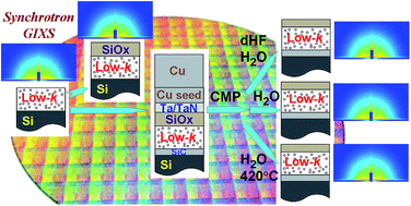
As integrated microelectronic circuit device dimensions continue to shrink, low dielectric constant (low-k) interlayer dielectrics are required for minimizing RC signal delay, capacitive coupling noise, and power consumption. The implementation of low-k materials in an interconnected structure, however, is known to be a very difficult task because of many criteria imposed by the structural functionality and the integration process. Here, we report structural reliability evaluation for the integration of low-k nanoporous organosillicate dielectrics into a multilayer structure, involving capping, chemical mechanical polishing (CMP), post-CMP cleaning, and thermal annealing processes. We have successfully investigated the structural reliability of the low-k dielectric layer subjected to such harsh processes using synchrotron grazing incidence X-ray scattering and reflectivity (GIXS and XR) analyses. This study additionally demonstrated that synchrotron GIXS and XR techniques are very powerful tools for providing valuable, accurate insight into the nanopore structure in low-k dielectric thin layers and the structural changes with the integration process conditions.


Introduction

Continuous improvements in device density and performance have been achieved by reducing feature size and scaling down device dimensions to the deep sub-micrometer level. The coupling of the inter-metal capacitance effect with line resistivity is now a limiting factor for the ultra-large-scale integration of electric circuits. To resolve this problem, it is necessary to have low dielectric constant (low-k) materials with insulation properties for the integration of copper (Cu) interconnects on high performance integrated circuits.1–4

One of the most critical challenges during the integration of low-k materials in damascene structure rises from the mechanical failures caused by scratching, peeling, and delamination during integration processes such as etching, resist stripping, chemical mechanical polishing (CMP), and post-CMP cleaning. During CMP and post-CMP cleaning, frictions associated with abrasive particles, polishing pressure and shear are known to cause mechanical damages, and chemical damages often occur due to the penetration of slurry residues (containing abrasive particles, slurry pH buffer, and electrolyte salts) and post-CMP cleaning chemicals into the pores of the dielectric layer.5–11 Such damages in the low-k dielectric layers are known to take place at the scales from micrometers to a few nanometers.12–16

Thus, damage-free processing and quantitative characterization of any possible damages of the complex interface system in damascene structure significantly dominate the reliability of multilevel interconnects and need to be clarified before practical implementations. In particular, the nanometer scale damages are quite difficult to analyze. Furthermore, evaluating the nanometer scale damages should be nondestructive and accurate, and involve simple yet non-invasive sample preparation.

In this study, we report the first structural reliability evaluation for the integration of low-k nanoporous polymethylsilsesquioxane (PMSSQ) dielectric layer into damascene structure using synchrotron grazing incidence X-ray scattering (GIXS) and X-ray reflectivity (XR), which are non-destructive analytical techniques. Low-k nanoporous PMSSQ film layers were prepared and then integrated into damascene structures with a bottom etching stop layer, a top capping layer, a diffusion barrier layer, a thin copper (Cu) seed layer and a thick Cu electroplating layer, followed by a series of damascene processes, namely CMP, post-CMP cleaning and annealing (Scheme 1). The synchrotron GIXS and XR analyses were successfully carried out on the low-k dielectric layers and the damascene-processed specimens, providing the structural details and changes at a subnanometer level. The non-destructive X-ray analyses confirmed that minor damages were caused by the damascene processes, particularly CMP and post-CMP cleaning with aqueous dilute hydrofluoric acid (dHF). The analyses further found the importance of the presence of a capping layer on the porous low-k materials as protection of the porous layer from CMP and post-CMP cleaning processes. In addition, this study demonstrated that synchrotron GIXS and XR are very powerful tools for evaluating the integration of low-k interdielectric layers into multilayer devices based on damascene processes.


image file: c5ra16983f-s1.tif
Scheme 1 Schematic cross-sections of the low-k nanoporous PMSSQ films (S1) and their stacks with other materials (S2; S3-a–c). The stacked specimens in a damascene structure were undergone CMP process and followed by post-CMP cleaning processes: S3-a, cleaned with dHF solution and subsequently with DI water; S3-b, cleaned with only DI water; S3-c, cleaned with only DI water and followed by thermal annealing at 400 °C for 3 h under vacuum. The cleaned S3-a and b stacks were further dried at 80 °C for 30 min.

Experimental part

A low-k precursor solution (HL02™, LG Chem. Ltd., Daejeon, Korea),17 which contained PMSSQ precursor and radially multi-branched porogen, was received from LG Chem; the porogen content was 30 wt% with respect to the PMSSQ precursor. The low-k precursor solution (5 wt% solid) was spin-coated on silicon (Si) wafers and followed by curing at 200 °C for 10 min and 420 °C for 1 h under nitrogen atmosphere. The resulting low-k nanoporous PMSSQ dielectric films (S1 in Scheme 1) were determined to have a refractive index of 1.28 at 633 nm, a dielectric constant of 2.25 at 1 MHz, and a modulus of 6.5 GPa.

In a previous study we found that silicate (SiOx) is a good protective capping layer material for low-k PMSSQ dielectric layer and, furthermore, its adhesion to the low-k dielectric layer can be improved significantly after a carbon dioxide (CO2) plasma treatment of the dielectric layer surface.18 Taking this fact into account, a 80 nm thick SiOx capping layer was deposited on the top of the CO2 plasma treated low-k dielectric layers by thermal deposition of tetraethoxysilane (TEOS) and put under subsequent curing at 400 °C for 2 h in nitrogen atmosphere (S2 in Scheme 1). To realize damascene low-k film stack, a multilayer stack structure, Si/SiC (30 nm thick)/low-k film (200 nm)/SiOx (80 nm)/tantalum (Ta, 5 nm)/tantalum nitride (TaN, 30 nm)/Cu seed (100 nm)/Cu (500 nm) was introduced. Here, SiC is a good candidate for an etch stop dielectric material in the damascene process. A Ta/TaN layer was deposited onto the SiOx layer as a barrier by consecutive physical vapour deposition (PVD) process. Cu seed layer was deposited onto the Ta/TaN barrier layer by PVD, followed by final Cu layer deposited via electrochemical deposition.

The Cu layer was removed out using a CMP polisher (Mirra, Applied Materials, Santa Clara, CA, USA) equipped with polyurethane pad (IC1000, Rodel-Nitta, Tokyo, Japan), and the SiOx layer was further over-polished in part at the same time for 30 nm-thick target. We used an orbital polishing tool with acidic slurry (SiO2 abrasive and H2O2 oxidant) for high-removal-rate under 1.5 psi. The Cu layer was removed in a three-step process: Cu removal with a high rate (200 nm min−1), Cu clearing with a medium rate (100 nm min−1), and barrier removal with a low rate (20 nm min−1).

The damascene-processed low-k dielectric film stacks were cleaned in three different ways to prevent Cu contamination and slurry residue. A set of the films stacks were cleaned with dHF solution (0.1 wt%) and followed by rinsing with dionized (DI) water and drying at 80 °C for 30 min (S3-a in Scheme 1). Another set of the film stacks were cleaned using only DI water and dried at 80 °C for 30 min (S3-b in Scheme 1). The other set of the film stacks were cleaned using only DI water and dried at 80 °C for 30 min, followed by thermal annealing at 400 °C for 3 h in a vacuum to completely remove all possible residual organics and absorbed water in the low-k layer (S3-c in Scheme 1).

Synchrotron GIXS measurements were performed at the 3C beamline19–22 of the Pohang Accelerator Laboratory (PAL), Pohang University of Science & technology. In the GIXS measurements, the sample-to-detector distance (SDD) was 1172 mm, and an X-ray source with a wavelength λ of 0.1608 nm and a two-dimensional (2D) charge-coupled detector (CCD: Mar USA, Evanston, IL, USA) were used. From the measured 2D GIXS patterns, one-dimensional (1D) scattering profiles were extracted at a vertical exit angle αf of 0.18° and a horizontal exit angle 2θf of 0.34° respectively. The obtained in-plane and out-of-plane GIXS profiles were quantitatively analyzed using GIXS formulas derived previously.19,23

Synchrotron XR measurements were carried out at the 3D beamline23–25 of PAL. An X-ray radiation source (λ = 0.154 nm) was used. The measured XR profiles were normalized to the intensity of the primary beam, which was monitored by an ionization chamber. The XR data were analyzed by a least square fitting procedure of parameterized model electron density profiles to the experimental data. In the XR data analysis we applied a recursive formula given by Parratt's dynamical theory,24,26 which properly incorporates absorption, refraction, and multiple scattering effects. Interfacial roughness was additionally determined by introducing Névot–Croce damping factors into the recursive formula, assuming Gaussian smearing functions.27

Results and discussion

The low-k dielectric films as well as the low-k stacks (Scheme 1) were examined using synchrotron GIXS technique to investigate their structures and structural changes after SiOx capping, CMP, post-CMP, cleaning and thermal annealing of which the details are described in Table 1. Fig. 1a shows a representative of the 2D GIXS patterns measured from the S1 film specimens (i.e., as-cured low-k nanoporous PMSSQ films). Similar 2D GIXS patterns were observed for the low-k dielectric film stacks. It features a weak structure factor around 2θf = 1° which is apparent in the in-plane scattering profiles shown in Fig. 1c. The weak but distinguishable structural interference originates not from ordering or random distribution but from the correlation between neighbouring pores in the films. The analysis of pore structure considered inter-pore structure factor with an approach using a hard sphere model and an approximation that the pores are locally monodispersed.19,28,29 As shown in Fig. 1c and d, the in-plane and out-of-plane scattering profiles could be satisfactorily fitted with the GIXS formula derived for spherical pore model; details of the GIXS formula and data analysis are given in ESI. The obtained pore size distributions are displayed in Fig. 1b. The analysis results collectively indicate that the pores generated in the low-k film layers were spherical and had a sharp interface with the PMSSQ matrix. The obtained structural parameters are summarized in Table 2.
Table 1 Process conditions after the integration for low-k films
Sample Process
CMP Post-CMP cleaning Post-CMP annealing
a Dilute hydrofluoric acid (0.1 wt%).b Deionized water.
S1
S2
S3-a Done dHFa + DI waterb
S3-b Done DI water
S3-c Done DI water 400 °C/30 min


image file: c5ra16983f-f1.tif
Fig. 1 (a) A representative of the measured 2D GIXS patterns, which was obtained at an incidence angle αi of 0.18° for a 200 nm thick nanoporous low-k film (S1 in Scheme 1); (b) pore radius r and distribution determined from the analysis of the GIXS data in (c) and (d); (c) in-plane GIXS profiles extracted along the qy direction (i.e., 2θf direction) at αf = 0.18° from the 2D GIXS patterns measured for the low-k film and the dielectric stacks in Scheme 1; (d) out-of-plane GIXS profiles extracted along the qz direction (i.e., αf direction) at 2θf = 0.34° from the 2D GIXS patterns of the low-k film and dielectric stacks. The symbols are the measured data and the solid lines represent fits to the data.
Table 2 GIXS and XR analysis results for low-k nanoporous PMSSQ dielectric layers and their integrated stack specimens
Specimen Pore size and size distribution Thickness (nm) Roughness (nm) Electron density (nm−3) Pk (%)
r0a (nm) σb [r with combining macron]c(nm) SiOx Low-k σsurff σinterfg SiOx Low-k
tsd tie ts ti ρe,sh ρe,ii ρe,avj ρe,s ρe,i ρe,av
a Pore radius determined from the peak maximum of the radius r and the size distribution σ of pores.b Width of the radius r and the size distribution of primary pores.c Average pore radius determined from the radius r and the size distribution of pores.d Thickness of skin layer.e Thickness of bulk layer.f Surface roughness.g Interfacial roughness between SiOx and low-k layer.h Electron density of skin layer.i Electron density of inner part.j Average electron density of film including both skin and bulk layer.k Relative porosity estimated from the electron density of the film with respect to the electron density (419 nm−3) of the PMSSQ film itself prepared without porogen loading.
S1 0.80 0.415 1.04 2.2 169.0 0.73   353 323 323 22.8
S2 0.80 0.415 1.04 1.7 77.4 2.7 167.4 0.50 1.60 619 593 594 476 323 325 22.3
S3-a 1.03 0.419 1.34 2.9 28.7 10.2 160.3 2.01 3.84 628 605 607 518 335 346 17.4
S3-b 0.90 0.415 1.17 3.1 30.0 11.0 161.7 1.03 3.82 626 599 593 516 326 338 19.3
S3-c 0.89 0.415 1.15 3.0 29.6 10.5 161.3 1.16 2.25 623 594 596 493 326 336 19.8


The low-k dielectric stack specimens were further subjected to XR analysis. As shown in Fig. 2a and b, the measured XR profiles present high frequency Kiessig fringes over the whole range of qz (= (4π/λ)sin[thin space (1/6-em)]θi, where θi is the grazing incidence angle of incoming X-ray beam with respect to the film plane) and additionally display the critical angles of the individual layers and the substrate at qz = 0.20 to 0.35 nm−1. The XR profiles were satisfactorily analyzed, using the Parratt algorithm.24,26 The XR analysis results are given in Table 2 and Fig. 2c and d.


image file: c5ra16983f-f2.tif
Fig. 2 X-ray reflectivity profiles measured for the low-k nanoporous PMSSQ film (S1) and dielectric stacks (S2, S3-a, S3-b and S3-c): (a) entire reflectivity profiles; (b) magnifications of the region of qz = 0.15° to 0.18° in (a). The symbols are the measured data and the solid lines represent fits to the data. Electron density profiles of entire range along the film thickness direction of the low-k film and the dielectric stacks, which were determined from the analysis of the data in (a) and (b): (c) entire profiles from Si substrate to air; (d) magnifications of the region around the low-k/SiOx interface and SiOx surface.

The as-cured low-k porous PMSSQ film was characterized by [r with combining macron] = 1.04 nm (average pore radius), ρe,av = 323 nm−3 (average electron density) and P = 22.8% (porosity with respect to the PMSSQ film itself as-cured without porogen loading) (S1 in Table 2). In addition, the presence of a very thin but relatively dense skin layer was confirmed; ts = 2.2 nm (thickness), ρe,s = 353 nm−3, σsurf = 0.73 nm (surface roughness). This skin layer might be formed by thermal curing of a portion of PMSSQ precursor itself, which was segregated toward the free surface from the PMSSQ precursor/porogen mixture. The ρe,s value of the skin layer, however, is still lower than that of the as-cured PMSSQ film (419 nm−3) without porogens.

The nanopores formed in the low-k dielectric layer were found to be preserved throughout the CO2 plasma treatment and SiOx capping layer deposition process (S2 in Table 2). A denser skin layer (ρe,s = 476 nm−3 and ts = 2.7 nm) was found to form in the low-k dielectric layer, however. Moreover, the skin layer in contact with the SiOx layer had an interfacial roughness σinterf of 1.60 nm, which was larger than the surface roughness before the CO2 plasma treatment and SiOx layer deposition. This denser skin layer with high interfacial roughness might originate from the CO2 plasma treatment, rather than the SiOx capping layer formation process.

The SiOx capping layer was characterized to have ρe,av of 594 nm−3, which was much higher than that of the low-k layer. A dense skin layer (ρe,s = 619 nm−3 and ts = 1.7 nm) was also confirmed to be present in the SiOx capping layer. The skin layer had σsurf = 0.50 nm, which was relatively smaller (i.e., smoother) than that of the low-k layer before the CO2 plasma treatment and SiOx deposition. In the S2 specimen, the SiC etching stop layer was additionally characterized to have an electron density ρe of 578 nm−3.

In the S3-a specimen, the SiOx capping layer revealed some changes in the skin layer. In fact, this skin layer was newly formed by the CMP and subsequent cleaning process after the damascene structure formation as shown in Scheme 1. The new skin layer was characterized to have ts = 2.9 nm, ρe,s = 628 nm−3 and σsurf = 2.01 nm. Overall, this skin layer was thicker, denser and rougher, compared to that formed in the as-prepared SiOx capping layer. Different from the skin layer, the inner part exhibited structural characteristics identical with those in the as-prepared SiOx capping layer. These results indicate that the CMP and subsequent cleaning process, including dHF cleaning, DI water rinsing and drying, inevitably generated a new skin layer but could not cause any changes in the main part of SiOx capping layer.

Similar new skin layer formations were observed in the S3-b and c specimens. The inner part of the SiOx layer was also confirmed to be unchanged but the ts values were slightly larger and the σsurf values were almost a half of that in the SiOx layer of the S3-a specimen. These different characteristics in the skin layers might be caused by the differences in the cleaning processes after the same CMP process. In fact, there were two differences in the cleaning processes: the usage of dHF solution for S3-a specimen and the thermal annealing at 400 °C for 3 h for S3-c specimen. The SiOx layers in the S3-b and c specimens showed similar skin layer features. These results collectively suggest that the skin layer formed in the SiOx capping layer of the S3-a specimen have experienced a certain level of chemical etching by the dHF solution used in the post-CMP cleaning process.

The results above collectively inform that the SiOx capping layer made an important role as the protection layer for the low-k nanoporous dielectric layer from the very harsh CMP process and the post-CMP cleaning processes.

Different from the SiOx layer, the low-k nanoporous dielectric layer in the damascene structures was found to have some discernible structural changes brought by the CMP and post-CMP cleaning processes, as shown in Fig. 1b–d and 2d and Table 2. In the S3-b specimen, the nanopores in the low-k layer experienced 12.5% increase in size and slightly broader size distribution. The skin layer was thickened by 307.4% and densified by 8.4%. σinterf, the roughness of the interface in contact with the SiOx capping layer, was also increased by 138.8%. Nevertheless, the main part of low-k layer revealed an electron density ρe,i of 326 nm−3, which is comparable to that of the unprocessed sample (323 nm−3). These results collectively indicate that the low-k layer in the damascene structure was intact under protection by the SiOx capping layer from the harsh CMP process but went under some sacrificial damages in a depth of 11 nm from the interface in contact with the SiOx layer by the CMP process. The damage with 11 nm depth might be attributed to the collapse of the nanopores under the downward and shear stresses generated during the CMP process. Due to the mechanically densified skin layer, the overall porosity P of the low-k layer was reduced to 19.3% from 22.8%.

The degree of damages was slightly more pronounced in the post-CMP cleaning process including dHF treatment (S3-a specimen). Furthermore, the main part of low-k layer became slightly dense after the cleaning process. These results suggest the usage of dHF solution in the post-CMP cleaning process causes a minor negative effect on the low-k layer. As a result, the P value of the low-k layer was further reduced to 17.4%.

Both the σinterf and ρe,s values were reduced and the ρe,i value remained unchanged in the S3-c specimen compared to those in the S3-b specimen. These values inform that the thermal-annealing after the DI water cleaning makes a positive contribution of reducing any damaged parts in the low-k layer in a certain level. Therefore, the P value of the low-k layer was slightly increased to 19.8%.

Overall, the GIXS and XR analysis results provide important features about the integration process of low-k nanoporous interdielectric layers into the multilayer microelectric devices fabricated by damascene process including very harsh CMP process and subsequent cleaning process as follows.

First, the SiOx layer, which can be fabricated from TEOS or any other sources, demonstrated excellent structural and chemical stability and further very good process compatibility to CMP process.

Second, the SiOx layer has proven its role and performance level as an excellent protection layer for low-k nanoporous dielectric layer. Despite the aid of SiOx protection layer, the CMP process caused the nanopores to collapse in the low-k layer with a depth of ca. 11 nm from the interface in contact with the SiOx protection layer. The results suggest that during the CMP process, the downward and shear stresses generated by the CMP were strong enough to penetrate with depth of 11 nm into the low-k layer through the SiOx protection layer. Thus, damage minimization in the low-k layer needs optimized CMP process with lesser downward and shear stresses, which may require longer processing time.

Third, the SiOx layer is a dielectric material and has a dielectric constant higher than that of the low-k layer. Therefore, SiOx layer with minimal thickness throughout the CMP process would bring improvements. It also may be eliminated via etching process as a post-CMP treatment if necessary.

Fourth, the usage of dHF in the post-CMP cleaning process was found to bring negative contribution to the low-k layer. DI water, however, was enough to clean out the undesired materials after the CMP process. Therefore, the usage of dHF is not recommended for the post-CMP cleaning process. Otherwise, dHF needs to be used sparingly or more dilute solution of HF may be used.

Fifth, the 400 °C thermal-annealing in vacuum in the post-CMP cleaning process was confirmed to bring positive contribution via eliminating any damages in the low-k layer caused by the harsh CMP process. Thus, thermal-annealing step is recommended as the final step of post-CMP cleaning process.

Finally, with the aid of SiOx capping layer the nanoporous PMSSQ dielectric material demonstrated an excellent feasibility as a low-k interdielectric layer candidate for the fabrication of advanced multilayer-structure microelectronic devices.

Conclusions

In this study, a low-k nanoporous PMSSQ dielectric material was successfully fabricated on Si substrates as damascene-structured multilayer stacks through the formations of a SiC etching barrier layer, a SiOx capping layer, a Ta/TaN barrier layer, a Cu seed layer and an electroplated Cu layer. The multilayer stacks were subjected to a damascene process, including very harsh CMP process and subsequent cleaning processes. The damascene-processed stack specimens were quantitatively characterized for the first time by using synchrotron GIXS and XR. These GIXS and XR analyses provided structural details on the damascene-processed dielectric stacks, which are essential for the structural reliability assessment of low-k nanoporous PMSSQ dielectric layer integration into advanced multilayer-structure microelectronic devices fabricated via a damascene-process based on CMP.

Overall, the low-k nanoporous PMSSQ dielectric with the aid of SiOx capping layer demonstrated excellent compatibility to the CMP, which is the mainly harsh step in the damascene process required in the production of advanced multilayer-structure microelectronic devices. Moreover, the PMSSQ dielectric retained its nanoporous structure throughout the CMP processes, providing advantageous low-k property essential for the reduced feature size and the scaled down device dimensions.

In addition, the strategy of combining the GIXS and the XR techniques was succeeded as a very powerful, nondestructive tool to assess low-k dielectric layer and its integration into microelectronic circuits in complex multilayer-structures.

Acknowledgements

This study was supported by the National Research Foundation (NRF) of Korea (Doyak Program 2011-0028678) and the Ministry of Science, ICT & Future Planning (MSIP) and the Ministry of Education (BK21 Plus Program and Global Excel Program). The synchrotron X-ray scattering and reflectivity measurements were supported by MSIP, POSTECH Foundation, and POSCO Company.

Notes and references

  1. The International Technology Roadmap for Semiconductors, Semiconductor Industry Association, San Jose, 2014 Search PubMed.
  2. S. Ma, Y. Wang, Z. Min and L. Zhong, Adv. Polym. Technol., 2013, 32, 21358 CrossRef PubMed.
  3. M. Morgen, E. T. Ryan, J.-H. Zhao, C. Hu, T. Cho and P. S. Ho, Annu. Rev. Mater. Sci., 2000, 30, 645–680 CrossRef CAS.
  4. K. Maex, M. R. Baklanov, D. Shamiryan, F. lacopi, S. H. Brongersma and Z. S. Yanovitskaya, J. Appl. Phys., 2003, 93, 8793–8841 CrossRef CAS PubMed.
  5. S. R. Roy, I. Ali, G. Shinn, N. Furusawa, R. Shah, S. Peterman, K. Witt, S. Eastman and P. Kumar, J. Electrochem. Soc., 1995, 142, 216–226 CrossRef CAS PubMed.
  6. L. Zhang, S. Raghavan and M. Weling, J. Vac. Sci. Technol., B: Microelectron. Nanometer Struct.–Process., Meas., Phenom., 1999, 17, 2248–2255 CrossRef CAS.
  7. K. Mosig, T. Jacobs, K. Brennan, M. Rasco, J. Wolf and R. Augur, Microelectron. Eng., 2002, 64, 11–24 CrossRef CAS.
  8. P. Leduc, T. Farjot, M. Savoye, A.-C. Demas, S. Maitrejean and G. Passemard, Microelectron. Eng., 2006, 83, 2072–2076 CrossRef CAS PubMed.
  9. M. Lépinay, N. Djourelov, H. Marinov, L. Broussous, K. Courouble, C. Licitra, F. Bertin, V. Rouessac and A. Ayral, J. Porous Mater., 2014, 21, 475–484 CrossRef.
  10. T.-S. Kim and R. H. Dauskardt, IEEE Trans. Device Mater. Reliab., 2009, 9, 509–515 CrossRef CAS.
  11. K. K. Lionti, W. Volksen, T. Magbitang, M. Darnon and G. Dubois, ECS J. Solid State Sci. Technol., 2015, 4, N3071–N3083 CrossRef CAS PubMed.
  12. T. Gross, S. Yao and S. Satyanarayana, Microelectron. Eng., 2008, 85, 401–407 CrossRef CAS PubMed.
  13. T.-S. Kim, T. Konno and R. H. Dauskardt, Acta Mater., 2009, 57, 4687–4696 CrossRef CAS PubMed.
  14. A. M. Lomonosov, A. Ayouch, P. Ruello, G. Vaudel, M. R. Baklanov, P. Verdonck, L. Zhao and V. E. Gusev, ACS Nano, 2012, 6, 1410–1415 CrossRef CAS PubMed.
  15. K. Vanstreels, C. Wu, P. Verdonck and M. R. Baklanov, Appl. Phys. Lett., 2012, 101, 123109 CrossRef PubMed.
  16. A. Uedono, P. Verdonck, A. Delabie, J. Swerts, T. Witters, T. Conard, M. R. Baklanov, S. V. Elshocht, N. Oshima and R. Suzuki, Jpn. J. Appl. Phys., 2013, 52, 106501 CrossRef.
  17. J. H. Cheong, G. G. Kang, M. J. Ko, J. W. Kang, M. S. Moon, B. R. Kim, B. G. Choi, D. H. Kang and J. M. Son, US Pat., 7,297,722 B2, 22 March 2011.
  18. K.-K. Choi, I. H. Cho, S. J. Park, J. E. Lim, O. J. Jung, J. H. Park, B. S. Min, S. B. Hwang, M. J. Ko and J. G. Lee, Thin Solid Films, 2007, 515, 5025–5030 CrossRef CAS PubMed.
  19. Y. Rho, B. Ahn, J. Yoon and M. Ree, J. Appl. Crystallogr., 2013, 46, 466–475 CrossRef CAS.
  20. B. Lee, Y.-H. Park, Y.-T. Hwang, W. Oh, J. Yoon and M. Ree, Nat. Mater., 2005, 4, 147–150 CrossRef CAS PubMed.
  21. B. Lee, W. Oh, Y. Hwang, Y.-H. Park, J. Yoon, K. S. Jin, K. Heo, J. Kim, K.-W. Kim and M. Ree, Adv. Mater., 2005, 17, 696–701 CrossRef CAS PubMed.
  22. B. Lee, J. Yoon, W. Oh, Y. Hwang, K. Heo, K. S. Jin, J. Kim, K.-W. Kim and M. Ree, Macromolecules, 2005, 38, 3395–3405 CrossRef CAS.
  23. K. Heo, S.-G. Park, J. Yoon, K. S. Jin, S. Jin, S.-W. Rhee and M. Ree, J. Phys. Chem. C, 2007, 111, 10848–10854 CAS.
  24. J. Bolze, M. Ree, H. S. Youn, S.-H. Chu and K. Char, Langmuir, 2001, 17, 6683–6691 CrossRef CAS.
  25. Y.-G. Ko, W. Kwon, H.-J. Yen, C.-W. Chang, D. M. Kim, K. Kim, S. G. Hahm, T. J. Lee, G.-S. Liou and M. Ree, Macromolecules, 2012, 45, 3749–3758 CrossRef CAS.
  26. L. G. Parratt, Phys. Rev., 1954, 95, 359–369 CrossRef.
  27. L. Névot and P. Croce, Rev. Phys. Appl., 1980, 15, 761–779 CrossRef.
  28. D. J. Kinning and E. L. Thomas, Macromolecules, 1984, 17, 1712–1718 CrossRef CAS.
  29. J. S. Pedersen, J. Appl. Crystallogr., 1994, 27, 595–608 CrossRef.

Footnotes

Electronic supplementary information (ESI) available: This article contains details of GIXS formula and data analysis. See DOI: 10.1039/c5ra16983f
K. Heo and B. J. Ree contributed equally to this study.

This journal is © The Royal Society of Chemistry 2015
Click here to see how this site uses Cookies. View our privacy policy here.