
Heterojunction photoanodes for solar water splitting using chemical-bath-deposited In2O3 micro-cubes and electro-sprayed Bi2WO6 textured nanopillars†
Bhavana Joshi‡
a,
Hyun Yoon‡a,
Hayong Kima,
Min-woo Kimab,
Mukund G. Malia,
Salem S. Al-Deyabc and
Sam S. Yoon*a
aSchool of Mechanical Engineering, Korea University, Seoul 136-713, Republic of Korea. E-mail: skyoon@korea.ac.kr
bGreen School, Korea University, Seoul, 136-713, Republic of Korea
cPetrochemicals Research Chair, Department of Chemistry, King Saud University, Riyadh 11451, Saudi Arabia
First published on 30th September 2015
Abstract
In2O3 micro-cubes were fabricated via chemical bath deposition (CDB) on an indium tin oxide (ITO) substrate, over which highly textured Bi2WO6 nanopillars were grown via a diffusion-and-aggregation phenomenon by electrostatic spraying deposition (ESD). The resulting heterojunction bilayer exhibited a photocurrent density value of 1.03 mA cm−2 under visible light of 100 mW cm−2 intensity. Widening the light absorptivity spectrum and reducing the charge recombination enhanced the performance of the heterojunction bilayer films for solar water splitting.
Introduction
Photoelectrochemical (PEC) cells are widely used for hydrogen production via solar water splitting. In order to improve the performance of PEC cells, various semiconductor-based photoelectrodes1,2 have been developed with high activities in the visible light spectrum. Bi-based compounds, which are photoactive in the visible light range, have been widely used because they are chemically stable and non-toxic.3,4 Bi is a p-block metal with d10 electronic configuration; hence, the Bi 6s orbital can hybridize with O 2p levels to form a hybrid valance band that enhances the mobility of photogenerated carriers and increases the photocatalytic activity of the material.5 Among various Bi oxides, Bi2WO6 has recently attracted attention for the relatively narrow bandgap (2.6–2.8 eV) and unique layered Aurivillius oxide structure,6 which efficiently uses visible light for photocatalysis. However, the actual utilization of this material is limited because of the propensity for recombination of charge carriers in devices made with it.7Various approaches have been attempted to overcome the problem of carrier recombination, such as doping,7 porous films,8 and bilayer structures.9 In particular, the use of heterojunction structures can promote the separation of electrons and holes and the absorption of photons, while further reducing the width of the bandgap. Heterojunction bilayer films using Bi2WO6 with Bi2O3,9 TiO2,10 WO3,11 and ZnWO4 (ref. 12) have been studied for use in the photodegradation of organic dyes and pollutants. However, to the best of our knowledge, the use of these bilayer films for solar water splitting has not yet been studied.
In2O3 is also an important p-block d10 metal oxide,13 suitable for photocatalysis and water splitting.14 In2O3 has a bandgap value of Eg ∼ 3.5 eV and has been used in solar cells, photovoltaics, optoelectronic devices, liquid crystal displays, and gas sensors.15 Recently, some studies regarding the nanostructure of In2O3 reported that the bandgap of the material could be lowered to 2.8 eV,16,17 which widens the absorption range of visible light for maximal water splitting and photocatalysis.
However, the water splitting performance of pure In2O3 is not very competitive, yielding a photocurrent density below 1 mA cm−2 in most cases. For this reason, the heterojunction structure with additional layers of other metal oxides has been commonly studied.18,19 There are two major advantages accompanying the introduction of the heterojunction bilayer structure. First, the heterojunction can widen the light absorption range by tuning the bandgap of the base material. Second, charge carrier recombination can be reduced by tuning the alignment of the bands. These synergetic effects can enhance the water splitting performance and hence the photoconversion efficiency.20 Liu et al.21 fabricated a bilayer film of In2O3/Bi2WO6 using electrospinning, but the application of the film was limited to the photodegradation of methyl-orange dye.
Herein, we demonstrate the fabrication of In2O3 micro-cubes via chemical bath deposition (CBD) on an indium tin oxide (ITO) substrate. Highly textured Bi2WO6 nano-pillars were grown on the surfaces of the In2O3 micro-cubes, creating an In2O3/Bi2WO6 heterojunction film. The process parameters were optimized to yield a heterojunction film with the best performance for water splitting.
Experimental methods
Precursors
Indium(III) nitrate (In(NO3)3, 98%, Sigma-Aldrich), urea (NH2CONH2, 99%, Samchun Chemical), bismuth(III) nitrate pentahydrate (BiN3O9·5H2O, ≥98%, Sigma-Aldrich), and tungsten(VI) ethoxide (C12H30O6W, 99.8%, 5% w/v in ethanol, Alfa Aesar), were used as precursors. Deionized (DI) water and propylene glycol (PG, C3H8O2, 99.0%, Duksan Chemical) were used as solvents for the deposition of In2O3 and Bi2WO6 films, respectively. All chemicals were used without further purification.Deposition of In2O3
The In2O3 films were formed by chemical bath deposition (CBD). Fifty mL of solution was prepared by mixing aqueous solutions of 0.05 M In(NO3)3 and 0.15 M urea in equal volumes. This solution was placed in a falcon tube; ITO-coated glass of size 2.5 × 2.5 cm2 was immersed in this tube and the tube was sealed. Thereafter, the tube was kept in a water bath maintained at 80 °C. Prior to the deposition of the films, the ITO-coated glass substrates were cleaned by ultrasonication in an ethanol bath and then dried. A schematic of the CBD process is shown in Fig. 1. The deposition of In2O3 films was performed for different deposition times as listed in Table 1. The films were air-annealed at 450 °C for 30 min to obtain crystallized and impurity-free In2O3 films.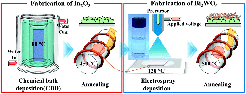 | ||
| Fig. 1 Schematics of CBD and ESD used for deposition of In2O3 and Bi2WO6, respectively. | ||
| Parameters | Conditions | |
|---|---|---|
| CBD | ESD | |
| Substrate | ITO | In2O3 films on ITO |
| Nozzle to substrate distance [cm] | — | 4.5 |
| Bath temperature [°C] | 80 | — |
| Substrate temperature [°C] | — | 120 |
| Flow rate [μl h−1] | — | 40 |
| Deposition time | 8, 12, 24, 36 [h] | 20, 40, 60, 80, 100, 120 [min] |
| Annealing temperature [°C] | 450 | 500 |
| Annealing time [min] | 30 | 10 |
Deposition of Bi2WO6
The Bi2WO6 films were formed by electrostatic spray deposition (ESD). The spray solution was prepared by mixing 0.1 M BiN3O9·5H2O in PG and adding an amount of C12H30O6W necessary to maintain a 2![[thin space (1/6-em)]](https://www.rsc.org/images/entities/char_2009.gif) :1 Bi:W ratio. The solution was stirred at a room temperature of 25 °C and appeared to be transparent with no precipitation for one week. The solution was further atomized by electrical forces to deposit the Bi2WO6 films. A schematic of ESD is shown in Fig. 1; the operating conditions used for the deposition of the films are presented in Table 1. The other details of ESD were reported in earlier papers.22,23 The bilayers were formed by electro-spraying the Bi2WO6 films for 20, 40, 60, 80, 100, and 120 min (henceforth Bi20, Bi40, Bi60, Bi80, Bi100, and Bi120) on CBD In2O3 films synthesized for different times of 8, 12, 24, and 36 h (henceforth In8, In12, In24, and In36).
:1 Bi:W ratio. The solution was stirred at a room temperature of 25 °C and appeared to be transparent with no precipitation for one week. The solution was further atomized by electrical forces to deposit the Bi2WO6 films. A schematic of ESD is shown in Fig. 1; the operating conditions used for the deposition of the films are presented in Table 1. The other details of ESD were reported in earlier papers.22,23 The bilayers were formed by electro-spraying the Bi2WO6 films for 20, 40, 60, 80, 100, and 120 min (henceforth Bi20, Bi40, Bi60, Bi80, Bi100, and Bi120) on CBD In2O3 films synthesized for different times of 8, 12, 24, and 36 h (henceforth In8, In12, In24, and In36).
The surface morphologies of the fabricated films were investigated using scanning electron microscopy (SEM, S-5000, Hitachi, Ltd). The crystalline structures of the films were characterized by X-ray diffraction (XRD, Rigaku Japan, D/MAX-2500, with Cu Kα X-rays). X-ray photoelectron spectroscopy (XPS, PHI5600, Physical Electronics) measurements were carried out to evaluate the chemical states of the films.
Photoelectrochemical measurements
Photocurrent measurements were performed under backside illumination and in a single-cell setup with a three-electrode configuration. In the setup, the bilayer film of the 0.5 × 0.5 cm2 irradiated area was the working negative electrode (anode), Ag/AgCl was the reference electrode, and Pt wire was the counter positive electrode (cathode). All electrodes were positioned near each other; the distances between them were maintained for all measurements. The electrolyte was a solution of 1 M KOH. Artificial sunlight from a Xe arc lamp (Newport, Oriel Instruments, USA) was used to illuminate the photoelectrode at a light intensity of 100 mW cm−2. An AM 1.5 filter was used to provide light with an intensity equivalent to one sun.Results and discussion
The X-ray diffraction spectra of pristine In2O3, Bi2WO6, and a bilayer of In2O3/Bi2WO6 are presented in Fig. 2. The XRD pattern in Fig. 2(a) clearly corresponds to the cubic In2O3 crystal structure. The diffraction peaks appearing at 21.52, 30.61, 35.59, 51.08, and 60.5° correspond to the (221), (222), (400), (440), and (622) planes, respectively, in good agreement with the JCPDS file 06-0416 for cubic In2O3. The strong diffraction peaks in Fig. 2(b) at 2θ = 28.36, 32.84, 47.10, and 57.12° correlate to the orthorhombic crystal planes of Bi2WO6; the pattern matches well with the JCPDS file 39-0256. Fig. 2(c) of the bilayer film clearly shows that the In2O3/Bi2WO6 heterostructure is well-integrated, reflecting phases of both orthorhombic Bi2WO6 and cubic In2O3. No peaks corresponding to traces of metal compounds mixed with Bi, In, and O are detected in the XRD patterns. Thus, the spectrum confirms that the In2O3/Bi2WO6 heterostructure is composed of separate phases of Bi2WO6 and In2O3. The ITO substrate peaks overlap with the peaks of In2O3. | ||
| Fig. 2 X-ray diffraction patterns of (a) pristine In2O3, (b) pristine Bi2WO6, and (c) In2O3/Bi2WO6 bilayer. | ||
The SEM images of pristine In2O3 films deposited by CBD shows the cubic morphology of the material, as seen in Fig. 3(a) and (d). Pillar-like structures (Fig. 3(b)) are observed in the cross-sectional image of the pristine Bi2WO6 film deposited by ESD, whereas the surface image of the same material (Fig. 3(e)) has a porous appearance, as the pillar spacing is large.23,24 Such pillar formation is unique to ESD fabrication, because of the simultaneous diffusive, thermophoretic, and electrophoretic transport of ESD particles. As the film grows, the electrostatic forces parallel to the substrate attract particles to the tips of pillars and repel particles in the valleys between pillars. Similar results were also observed in an earlier examination of BiVO4 films fabricated by ESD.24 Thus, it is clear that pillar formation by ESD is uniquely characteristic of Bi-based oxides. The cross-sectional SEM image of the bilayer film shows that the surface is composed of many uniform structures of pillars on cubes (Fig. 3(c)), similar to the pristine films. The surface-view SEM image shows the Bi2WO6 pillars coated over different cubes of In2O3. The image also shows an empty area resulting from repulsion between Bi2WO6 pillars, which excluded Bi2WO6 particles from filling the empty area, as mentioned above. This unique cube and pillar morphology allows light absorption deep in the In2O3 film and increases both the surface area and charge separation.
 | ||
| Fig. 3 Cross-sectional and surface SEM images of (a and d) pristine In2O3, (b and e) pristine Bi2WO6, (c and f) bilayer In24–Bi80. | ||
The chemical states of constituent elements for the bilayer, investigated by XPS, are presented in Fig. 4. The XPS survey spectrum of the bilayer film, presented in ESI Fig. S1,† confirms the coexistence of In2O3 and Bi2WO6 in the obtained sample. The binding energies for Bi 4f7/2 and Bi 4f5/2, shown in Fig. 4(a), are 159.1 and 164.4 eV, attributed to Bi3+ and Bi4+. The peaks centered at 35.4 and 37.54 eV (Fig. 4(b)) are assigned to W 4f5/2 and W 4f7/2 respectively.25 The presence of In3+ is confirmed by the peaks at 444.6 and 452.2 eV, corresponding to the 3d5/2 and 3d3/2 spin orbits of In shown in Fig. 4(c), which confirms the formation of In2O3.26 The peak located at 530.2 eV is assigned to O 1s in Fig. 4(d).
 | ||
| Fig. 4 XPS (a) Bi 4f, (b) W 4f, (c) Si 2p, and (d) C 1s spectra for bilayer In24–Bi80. | ||
The photocurrent value obtained in the bilayer electrode is positive, indicating the formation of an n-type photoanode. Thus, the generated photocurrent correlates directly to the oxygen evolution. To investigate the influence of individual layer thicknesses on the photocurrent generated by In2O3/Bi2WO6 heterojunction films, linear scan voltammograms were recorded of the different samples. Fig. 5 shows a plot of photocurrent density versus the applied potential for various Bi2WO6 thicknesses coated on 24 h CBD-coated In2O3. The samples were illuminated with one sun (100 mW cm−2) intensity of light. The plot clearly reveals that the photocurrent increases as the Bi2WO6 deposition time increases, reaching a maximum at 80 min and thereafter decreases for further increases in coating time. The value of photocurrent density (PCD) measured for the maximum case of In24–Bi80 is 1.03 mA cm−2, which is almost double than that of pristine In2O3 and 20 times greater than that of pristine Bi2WO6, as shown in ESI Fig. S2.† The higher photocurrent density of the In24–Bi80 film relative to those of the pristine materials results from the lower-energy bandgap of the bilayer film, which increases the light absorption. In addition, the formation of the In2O3/Bi2WO6 heterojunction increases the effective electron/hole separation. However, further increase in Bi2WO6 spray time above 80 min lowers the photocurrent generated from the bilayer. The increased height of the Bi2WO6 pillars increases the transport length of the charge carriers. The electric field also decreases in the bulk and the interface of the bilayers with increasing pillar length, which leads to the recombination of charge carriers. Thus, for higher Bi2WO6 deposition times of 100 or 120 min, the photocurrent falls to 0.8 mA cm−2 and 0.6 mA cm−2, respectively. The onset potential for all bilayer films is observed to be −0.1 V, which is much lower than that of pristine Bi2WO6 (shown in ESI Fig. S2†). The inset image shows the photocurrent at 0.7 V (vs. Ag/AgCl) for different Bi2WO6 spray times.
 | ||
| Fig. 5 Current–voltage curve of 24 h-coated In2O3 layered with various Bi2WO6 thicknesses. | ||
The photocurrent density (PCD) of bilayer films with variation in the thickness of the In2O3 base layer is shown in Fig. 6. In all cases, the Bi2WO6 was sprayed for 80 min. The PCD value is observed to increase from 8 h to 24 h of In2O3 deposition. The maximum PCD achieved is 1.03 mA cm−2 from the In24–Bi80 bilayer film. However, further increase in the In2O3 thickness results in a decrease in the PCD. This decrease results from the recombination process, which becomes dominant after the optimal thickness is exceeded. Thus, films deposited for 36 h have higher thicknesses, which increase the transport path lengths of the photogenerated charge carriers; simultaneously, the applied electric field becomes weak in the bulk material, driving the recombination of electron/hole pairs and reducing the PCD.
 | ||
| Fig. 6 Photocurrent density curve of bilayer with 80 min deposited Bi2WO6 on varied thicknesses of In2O3. | ||
As shown, the bilayer films exhibit higher photocurrents as compared to the pristine materials. In the pristine films, In2O3 and Bi2WO6 are limited in light absorption capacity; additionally, photogenerated hole/electron pairs recombine quickly. However, in the bilayer films, better results are observed because of the relative energy band positions of the component semiconductor materials. The bandgap energy values of the pristine Bi2WO6 and In2O3 films were extrapolated from the Tauc plot, which yielded 2.7 and 2.5 eV, respectively.27,28 The bandgap energy of the In24–Bi80 bilayer film was 2.4 eV, which is in agreement with the value reported by Liu et al.21 This reduced bandgap is favorable to absorb the increased range of the light spectrum. Note that the conduction band (Ecb) and valance band (Evb) edge positions can be determined by using the empirical formula such as, Ecb = Evb − Eg and Evb = X − 4.5 + 0.5Eg, where X is the absolute electronegativity, 4.5 eV is the energy of free electrons on a hydrogen scale.29,30 As shown in Fig. 7, under the illuminated condition both oxides absorb light to generate electron/hole pairs in the different layers. The conduction band edge potential of In2O3 is more negative than that of Bi2WO6, which forbids the direct transport of photogenerated electrons from Bi2WO6 to In2O3. Meanwhile, the valance band maximum of In2O3 is close to the conduction band minimum of Bi2WO6; thus, the photogenerated holes in In2O3 and electrons in Bi2WO6 are recombined. Hence, all holes generated in Bi2WO6 are used for water oxidation, while the electrons in In2O3 are transferred to the counter electrode. In2O3/Bi2WO6 bilayer films such as those synthesized in this study may provide improved energetics for the reduction of electrons on the counter electrode. Thus, the overall electron/hole separation efficiency is enhanced. Introducing the heterojunction film structure also decreases the onset potential of the photocurrent and increases the degree of charge separation. A similar mechanism is observed in the case of BiVO4 deposited on an n-type Si substrate.31 Thus, the deposited n/n heterojunction bilayer film shows enhancement in photocurrents at the optimized film layer thicknesses.
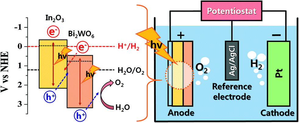 | ||
| Fig. 7 Mechanism of charge separation in bilayer film. | ||
The stability of the In24–Bi80 bilayer film was tested using the chronoamperometry technique where the photocurrent was measured at a potential of 0.2 V (vs. Ag/AgCl). In Fig. 8, the photocurrent value of 0.5 mA cm−2 remains constant for 60 min under one-sun illumination of 100 mW cm−2. This constant photocurrent value confirms the photostability of the bilayer film. This result is also consistent with the photocurrent obtained using the linear voltammetry scan for the In24–Bi80 film shown in Fig. 6. This consistent and stable photocurrent confirms that Bi2WO6 nanopillars on top remains intact with the In2O3 layer below even after 1 h light illumination.
 | ||
| Fig. 8 Photocurrent stability curve of bilayer film at a potential of 0.2 V (vs. Ag/AgCl). | ||
Conclusions
In2O3/Bi2WO6 bilayer films were prepared successfully by utilizing CBD and ESD methods. The deposited films showed unique pillar-coated cubic morphologies with increased surface area. The XRD and XPS spectra confirmed the presence of the individual component phases in the heterojunction film; no other intermetallic phases were observed. The optimized thickness of both films was reflected in the highest photocurrent of 1.03 mA cm−2 at 0.7 V. The mechanism described for n/n bilayer heterojunction films clarifies the reason that better electron/hole separation occurs in films that are narrow in the pristine state.Acknowledgements
This research was supported by NRF-2013R1A2A2A05005589, Special International Collaboration and Post-Doctoral Fellowship funded by Korea University. This research was also supported by the Commercializations Promotion Agency for R&D Outcomes (COMPA) funded by the Ministry of Science, ICT and Future Planning (MISP). The authors extend their appreciation to the Deanship of Scientific Research at King Saud University for its funding this Prolific Research group (PRG-1436-03).References
- J. Luo, S. D. Tilley, L. Steier, M. Schreier, M. T. Mayer, H. J. Fan and M. Grätzel, Nano Lett., 2015, 15, 1395–1402 CrossRef CAS PubMed.
- W. Sheng, B. Sun, T. Shi, X. Tan, Z. Peng and G. Liao, ACS Nano, 2014, 8, 7163–7169 CrossRef CAS PubMed.
- Y. Wang, Y. Wang, Y. Meng, H. Ding, Y. Shan, X. Zhao and X. Tang, J. Phys. Chem. C, 2008, 112, 6620–6626 CAS.
- S.-J. Liu, Y.-F. Hou, S.-L. Zheng, Y. Zhang and Y. Wang, CrystEngComm, 2013, 15, 4124–4130 RSC.
- C. Liao, Z. Ma, G. Dong, J. Qiu and R. J. Xie, J. Am. Ceram. Soc., 2015, 98, 957–964 CrossRef CAS PubMed.
- Y. F. Hou, S. J. Liu, J. H. Zhang, X. Cheng and Y. Wang, Dalton Trans., 2014, 43, 1025–1031 RSC.
- R. Cao, H. Huang, N. Tian, Y. Zhang, Y. Guo and T. Zhang, Mater. Charact., 2015, 101, 166–172 CrossRef CAS PubMed.
- L.-W. Zhang, Y.-J. Wang, H.-Y. Cheng, W.-Q. Yao and Y.-F. Zhu, Adv. Mater., 2009, 21, 1286–1290 CrossRef CAS PubMed.
- Y. Peng, M. Yan, Q.-G. Chen, C.-M. Fan, H.-Y. Zhou and A.-W. Xu, J. Mater. Chem. A, 2014, 2, 8517–8524 CAS.
- G. Colon, S. Murcia Lopez, M. C. Hidalgo and J. A. Navio, Chem. Commun., 2010, 46, 4809–4811 RSC.
- M.-S. Gui, W.-D. Zhang, Y.-Q. Chang and Y.-X. Yu, Chem. Eng. J., 2012, 197, 283–288 CrossRef CAS PubMed.
- D. He, L. Wang, D. Xu, J. Zhai, D. Wang and T. Xie, ACS Appl. Mater. Interfaces, 2011, 3, 3167–3171 CAS.
- N. Arai, N. Saito, H. Nishiyama, Y. Shimodaira, H. Kobayashi, Y. Inoue and K. Sato, J. Phys. Chem. C, 2008, 112, 5000–5005 CAS.
- Y. Sun, C. Murphy, K. Reyesgil, E. Reyesgarcia, J. Lilly and D. Raftery, Int. J. Hydrogen Energy, 2008, 33, 5967–5974 CrossRef CAS PubMed.
- A. K. Chakraborty and M. A. Kebede, J. Cluster Sci., 2011, 23, 247–257 CrossRef.
- A. Walsh, J. L. F. Da Silva, S.-H. Wei, C. Körber, A. Klein, L. F. J. Piper, A. DeMasi, K. E. Smith, G. Panaccione, P. Torelli, D. J. Payne, A. Bourlange and R. G. Egdell, Phys. Rev. Lett., 2008, 100, 167402 CrossRef.
- D. V. Shinde, D. Y. Ahn, V. V. Jadhav, D. Y. Lee, N. K. Shrestha, J. K. Lee, H. Y. Lee, R. S. Mane and S.-H. Han, J. Mater. Chem. A, 2014, 2, 5490–5498 CAS.
- J. Mu, B. Chen, M. Zhang, Z. Guo, P. Zhang, Z. Zhang, Y. Sun, C. Shao and Y. Liu, ACS Appl. Mater. Interfaces, 2012, 4, 424–430 CAS.
- Z. Wang, B. Huang, Y. Dai, X. Qin, X. Zhang, P. Wang, H. Liu and J. Yu, J. Phys. Chem. C, 2009, 113, 4612–4617 CAS.
- S. Choudhary, S. Upadhyay, P. Kumar, N. Singh, V. R. Satsangi, R. Shrivastav and S. Dass, Int. J. Hydrogen Energy, 2012, 37, 18713–18730 CrossRef CAS PubMed.
- X. Liu, Q. Lu, C. Wang, C. Zhu and S. Liu, J. Sol-Gel Sci. Technol., 2014, 73, 358–364 CrossRef.
- H. Yoon, J. H. Woo, Y. M. Ra, S. S. Yoon, H. Y. Kim, S. Ahn, J. H. Yun, J. Gwak, K. Yoon and S. C. James, Aerosol Sci. Technol., 2011, 45, 1448–1455 CrossRef CAS PubMed.
- H. Yoon, M. G. Mali, J.-Y. Choi, M.-W. Kim, S. K. Choi, H. Park, S. S. Al-Deyab, M. T. Swihart, A. L. Yarin and S. S. Yoon, Langmuir, 2015, 31, 3727–3737 CrossRef CAS PubMed.
- M. G. Mali, H. Yoon, M.-W. Kim, M. T. Swihart, S. S. Al-Deyab and S. S. Yoon, Appl. Phys. Lett., 2015, 106, 151603 CrossRef PubMed.
- M. Ge, Y. Li, L. Liu, Z. Zhou and W. Chen, J. Phys. Chem. C, 2011, 115, 5220–5225 CAS.
- D. V. Shinde, V. V. Jadhav, D. Y. Lee, N. K. Shrestha, J. K. Lee, H. Y. Lee, R. S. Mane and S.-H. Han, J. Mater. Chem. A, 2014, 2, 5490–5498 CAS.
- G. Zhang, Z. Hu, M. Sun, Y. Liu, L. Liu, H. Liu, C.-P. Huang, J. Qu and J. Li, Adv. Funct. Mater., 2015, 25, 3726–3734 CrossRef CAS PubMed.
- M. G. Mali, H. Yoon, H. Kim, B. N. Joshi, S. S. Al-Deyab and S. S. Yoon, ChemPhysChem, 2015 DOI:10.1002/cphc.201500636.
- Y. Xu and M. A. Schoonen, Am. Mineral., 2000, 85, 543–556 CrossRef CAS.
- H. Cheng, B. Huang, P. Wang, Z. Wang, Z. Lou, J. Wang, X. Qin, X. Zhang and Y. Dai, Chem. Commun., 2011, 47, 7054–7056 RSC.
- H. Jung, S. Y. Chae, C. Shin, B. K. Min, O.-S. Joo and Y. J. Hwang, ACS Appl. Mater. Interfaces, 2015, 7, 5788–5796 CAS.
Footnotes |
| † Electronic supplementary information (ESI) available. See DOI: 10.1039/c5ra16833c |
| ‡ Equal contribution. |
| This journal is © The Royal Society of Chemistry 2015 |