Reduced surface defects of organometallic perovskite by thermal annealing for highly efficient perovskite solar cells

Peng Cuia, Pengfei Fua, Dong Weia, Meicheng Li*ab, Dandan Songa, Xiaopeng Yuea, Yaoyao Lia, Zhirong Zhanga, Yingfeng Lia and Joseph Michel Mbenguea
aState Key Laboratory of Alternate Electrical Power System with Renewable Energy Sources, School of Renewable Energy, North China Electric Power University, Beijing 102206, China. E-mail: mcli@ncepu.edu.cn; Fax: +86 10 6177 2951; Tel: +86 10 6177 2951
bChongqing Materials Research Institute, Chongqing 400707, China

Received 18th August 2015 , Accepted 1st September 2015

First published on 1st September 2015


Abstract

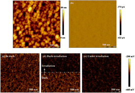
The surface defects of the organometallic perovskite play an important role in the photovoltaic performance of solar cells, which depress the conversion efficiency and cause photocurrent hysteresis. As a key step in fabricating perovskite solar cells, the heating step possibly modifies the surface defects, which in turn leads to the modified device performance. In this context, the surface defects of the organometallic perovskite (CH3NH3PbI3) and their modification by thermal annealing are investigated. It is revealed that the surface defects create electron traps which can be reduced by thermal annealing. Consequently, the perovskite solar cells exhibit improved conversion efficiency from 10.9% to 17.1% with the thermal annealing temperature of the perovskite increasing from 60 °C to 130 °C. The photocurrent hysteresis of the solar cells is also subdued. This work provides further insights into the function of thermal annealing by modifying surface defects, which also favors the exploration of the perovskite solar cells with high-efficiency and eliminated photocurrent hysteresis.


Introduction

Thin film solar cells are a kind of promising photovoltaic technology for energy conversion due to their unique properties including low material-consumption, mechanical flexibility and the potential for various applications. However, most thin film solar cell techniques face either low energy conversion efficiencies or higher processing/material costs.1,2 Recently, perovskite solar cells, with mixed organic–inorganic halide perovskites (MAPbX3, MA = CH3NH3, X = I, Cl, Br) as absorbers, offer tempting prospects on both energy conversion efficiency and processing/material costs.2–8 The conversion efficiency of the perovskite solar cells has achieved over 20% from less than 5% since 2009.3–8

The solution-processing ability of the perovskite material, as one of its main advantages, makes its deposition much simple requiring only a simple heating step to convert the deposited precursor solution to the polycrystalline perovskite form.6–9 The heating step in preparing the perovskite film is crucial in improving the film quality for efficient solar cells, which can improve the coverage, the grain size and the doping property of the perovskite films.10–13 Meanwhile, correlating with the polycrystalline nature of the solution-processed perovskite, the surface defects present at the perovskite surface, which are found to act as trap states for carrier trapping and are one important origin for the trap states in the perovskite films,14 leading to the depressed conversion efficiency and the deteriorated photocurrent hysteresis.15–17 As the heating step can modify the doping profile of the perovskite, i.e., the defects inner the perovskite film,12,13 it is also possibly able to modify the surface defects of the perovskite. Though many studies investigate in the heating step and its effect on the photovoltaic performance of the solar cells, which focus on the bulk evolution and are of crucial importance for highly efficient solar cells,10–13 the exploration of the influence of heating step on the surface defects and the resultant performance of the related solar cells is still lacked.

In this context, the effect of the heating step, i.e., the thermal annealing temperature and time, on the surface defects of the perovskite (MAPbI3) is investigated with kelvin probe microscope (KPFM) and conductive atomic force scope (C-AFM). It is found that the surface defects create electron traps at the MAPbI3 surface, which can be suppressed by the heating step. Consequently, the solar cell with MAPbI3 film annealed at high temperature possesses high power conversion efficiency and subdued photocurrent hysteresis.

Experimental

Fabrication of MAPbI3 film

MAPbI3 films were fabricated using a sequential deposition process.7,9 PbI2 was first dissolved in dimethylsulfoxide (DMSO) or dimethyl formamide (DMF) solutions (1 mol ml−1) and then kept at 70 °C for one day to achieve intensive dissolution. Then PbI2 solution was filtered with a 0.45 μm filter and loaded on compact TiO2 layer (for solar cells) or FTO/glass substrates (KPFM and C-AFM measurements) by spin-coating at a speed of 3000 rpm for 30 s repeated for 3 times. After that, yellow PbI2 films, without additional thermal annealing, were dipped into the solution of MAI (40 mg ml−1) in ultra-dry isopropanol for 10 min, which leads to the formation of MAPbI3 films. Consequently, MAPbI3 films were rinsed with neat ultra-dry isopropanol to remove excess MAI and post-annealed at different temperatures and time. All of the procedures were carried out in the glove box filled with high purity N2.

Solar cell fabrication

The solar cells employ the planar architecture of FTO/compact TiO2/MAPbI3 (∼300 nm)/hole transport material (HTM)/Au electrode. FTO/glass substrates were pre-cleaned and treated by UV-ozone for 15 min before solar cell fabrication. Compact TiO2 layer with a thickness of approximately 25 nm was fabricated on FTO by TiCl4 treatment (22 μl in 1 ml deionized water) at 70 °C for 60 min.18 HTM layer (150 nm) was obtained by spin-coating the 2,2′,7,7′-tetrakis[N,N-di(4-methoxyphenyl)amino]-9,9′-spirobifluorene (spiro-MeOTAD) solution (80 mg ml−1 dissolved in chlorobenzene) with the standard additives tert-butylpyridine (28.5 μl in 1 ml chlorobenzene) and lithiumbis(trifluoromethanesulfonyl)imide (8.75 mg ml−1) at a speed of 5000 rpm for 30 s repeated for 2 times in the glove box, followed by degradation in clean air for 6 h. After that, Au electrode with a thickness of 120 nm was prepared by magnetron sputtering.

Characterization

KPFM and C-AFM were carried out using Agilent SPM 5500 with the sample chamber filled with high purity N2. The MAPbI3 samples were immediately transferred to the chamber after taking out from glove box and hold for 10 min in N2 atmosphere before the measurement to avoid the effects of oxygen and moisture. KPFM was measured in the tapping mode. C-AFM was conducted in the contact mode with the sample grounded. No voltage was applied between the sample and the tip. The irradiation of the samples was conducted using a Xe lamp with the light output coupled by a fiber inserted in the sample chamber. Current density–voltage curves of the solar cells were measured using a source meter (Keithley 2400) under AM 1.5G irradiation with a power density of 100 mW cm−2 from a solar simulator (XES-301S+EL-100).

Results and discussion

The topographic image of the MAPbI3 film without thermal annealing characterized by atomic force microscope (AFM) is shown in Fig. 1a, which exhibits the typical polycrystalline structure with multiple small grains. To study the electronic property of the surface defects at the MAPbI3 surface, C-AFM which measures the current flowing between the tip and the sample was employed. The photogenerated holes and/or electrons under irradiation from Xe lamp lead to the measured photocurrent by the tip. During the measurements, the sample was grounded and the detection of a negative current indicates the presence of photo-induced current.19 Fig. 1b shows the corresponding current spatial map of the as-prepared MAPbI3 film. A negative current flow is obtained, proving the generation of photo-induced current as no electric field was added. The photogenerated current is collected from MAPbI3 surface, hence, the variation in the photogenerated current indicate the difference in the efficacy of the carrier collection from MAPbI3 surface, which can reflects the amount of the surface defects.
image file: c5ra16669a-f1.tif
Fig. 1 (a) The topography map and (b) the current map of MAPbI3 films without thermal annealing; (c–e) the surface potential maps of MAPbI3 films under different irradiation conditions.

To investigate the role of the surface defects at MAPbI3 surface, KPFM, as one efficient tool to characterize the surface defects,20–22 is employed. KPFM measures the local contact potential difference (LCPD) between the sample and the tip, which is defined as:

image file: c5ra16669a-t1.tif
where φtip and φsample are the work function of the tip and the surface potential of the sample, respectively, and e is the electronic charge. The surface potential of MAPbI3 is varied in presence of surface defects, which shift up or down the surface potential according to trapping electrons or holes. The potential image of neat MAPbI3 film without annealing measured in dark is shown in Fig. 1c. The potential is spatially different, corresponding to the different distributions of the surface defects. Under irradiation, as presented in Fig. 1d and e, the overall potential is lowered, which indicates the accumulation of photogenerated holes at the surface. Hereby, the photogenerated current measured by C-AFM is caused by the hole current.

MAPbI3 films annealed at different temperatures and different time were prepared and their topographic images are shown in Fig. 2a–c. It is clear that the grain size increases with increasing annealing temperature and time, due to the inter-diffusion of the grains. This observation is similar to the previous reports on the evolution of the MAPbI3 film morphology on the annealing parameters.10–12 KPFM images are shown in Fig. 2d–f. The potential increases with the annealing temperature and time, which increases more than 100 mV from the film without annealing (Fig. 1c) to the film annealed at 130 °C (Fig. 2f). The current maps from C-AFM shown in Fig. 2g–i reveal that the photogenerated current also increases (corresponding to a deep color) with the annealing temperature and time.


image file: c5ra16669a-f2.tif
Fig. 2 (a–c) Topographic images, (d–f) potential images and (g–i) current maps of MAPbI3 films fabricated at different annealing parameters, (a, d and g) annealed at 100 °C for 30 min; (b, e and h) annealed at 100 °C for 60 min; (c, f and i) annealed at 130 °C for 30 min.

From Fig. 1, it is proved that the photocurrent collected by C-AFM is caused by photogenerated holes. So the increased photocurrent with increasing annealing temperature and time shown in Fig. 2 implies a large number of photogenerated holes collected from MAPbI3 surface at high annealing temperature and long annealing time. According to potential images measured by KPFM shown in Fig. 2, the enhanced hole collection is accompanied by the increase of the surface potential, suggesting that the surface defects act as the electron traps at the surface instead of hole traps which cause the decreased potential. The identification of the trap states to electron traps here is in accordance with the evidences from the calculation result using density functional theory23 and the deduction from the experimental current–voltage behaviors of the perovskites24 in previous reports. Hence, from KPFM and C-AFM measurements, it can be deduced that the surface defects are diminished with increasing annealing temperature and time, which reduces the number of the trap levels lying in the bandgap and suppresses the recombination between the trapped electrons and free holes, leading to the increased potential and the enhanced hole collection.

To further reveal the reduced trap states at the surface by thermal annealing, photoluminescence (PL) spectra of the MAPbI3 films without and with annealing were measured. As shown in Fig. 3a, the MAPbI3 film without annealing shows an obvious emission peak located around 778 nm, whereas the annealed MAPbI3 film exhibits one main peak located at 753 nm. The emission peak located at the long wavelength of 778 nm corresponds to the emission from the spontaneous radiative recombination between the trap states,15 which shows a red-shifted emission peak compared with that from the band edge transition (753 nm), as depicted in Fig. 3b. The decreased emission intensity of the trap-involved luminescence of the annealed MAPbI3 again proves the reduced trap states by thermal annealing.


image file: c5ra16669a-f3.tif
Fig. 3 (a) Photoluminescence (PL) spectra of MAPbI3 films without and with annealing at 130 °C for 30 min. Inset shows the peak from the trap-involved luminescence extracted from the PL spectra by Gaussian Fitting. (b) Schematic illustration of the band energy level and the PL from MAPbI3 films.

The increases of the LCPD from KPFM and the photocurrent from C-AFM are accompanied with the increased grain size of MAPbI3 film, as depicted in the top view images measured by AFM (Fig. 2) and scanning electron microscope (SEM) (Fig. 4). MAPbI3 film without thermal annealing (Fig. 4a) shows small grains, which are uncompacted on the substrate as in accordance with the AFM image in Fig. 1a. With increasing annealing temperature from 60 °C to 130 °C (Fig. 4b–d), the grain size gradually increases from several tens of nanometers to hundreds of nanometers, which is consistent with the trend characterized by AFM. The increased grain size with increasing annealing temperature can be ascribed to the Ostwald ripening during the thermal annealing, which leads to the growth of the large grains and the vanishing of the small grains through the inter-diffusion among the grains. As MAPbI3 film with a large grain size yields less grain boundaries, it may be speculated that the variations of the LCPD from KPFM and the photocurrent from C-AFM are caused by the increased grain size other than the reduced surface defects.


image file: c5ra16669a-f4.tif
Fig. 4 Top view SEM images of MAPbI3 films fabricated from different solvent (DMSO, DMF) and annealing temperature (none, 60–130 °C). (a)–(f) The different parameters as labeled on the images.

To investigate the role of the grain size, MAPbI3 films fabricated from PbI2 dissolved in different solvents (DMF in addition to DMSO) but annealed at same parameters are characterized and compared. SEM images of the MAPbI3 film with PbI2 fabricated from DMF solvent (DMF-MAPbI3) are shown in Fig. 4e and f, which clearly reveals the larger grain size of DMF-MAPbI3 than that of the MAPbI3 film with PbI2 fabricated from DMSO solvent (DMSO-MAPbI3), as is in accordance with the previous report.9 The topography maps characterized by AFM are shown in Fig. 5a and b, from which it is also clear that DMF-MAPbI3 film possesses a larger grain size. Fig. 5c and d show the corresponding KPFM images of the MAPbI3 films. The overall potential difference between the DMF-MAPbI3 and DMSO-MAPbI3 is less than 50 mV, which is much smaller than that among the films annealed at different annealing parameters (large than 100 mV) shown in Fig. 2, despite of the more obvious difference in the grain size in the former in the former. Meanwhile, the current difference is also much smaller between the DMF-MAPbI3 and DMSO-MAPbI3, as shown in Fig. 5e and f. Hence, the effect of the grain size on the variations of the potential and photocurrent with the annealing parameters is not the main origin for the varied LCPD and photocurrent.


image file: c5ra16669a-f5.tif
Fig. 5 Topography (a and b), potential (c and d) and current (e and f) images of the MAPbI3 films fabricated from PbI2 dissolved in DMF (a, c and e) and DMSO solvent (b, d and f), respectively.

Therefore, the increased potential and photocurrent detected by KPFM and C-AFM, respectively, are mainly caused by the reduced surface defects. The origin of the surface defects is probably the exposed I atoms with dangling bonds, due to low surface energy of I atoms in MAPbI3. In addition, the sequential deposition induces excess MAI in the film, especially near the surface, which also causes the richness of I atoms in MAPbI3. These dangling bonds tend to trap electrons to form the saturated bonds, followed by the recombination with the holes under irradiation. In condition of the high annealing temperature, the surface I atoms are thermal motivated, which can be released from the surface of MAPbI3 by combination with other I atoms due to the low sublimation temperature of I2 or MA+. Moreover, the thermal annealing also favours the reconstruction of the MAPbI3 surface, which also decreases the structural defects at the surface. Hence, at high temperature, the surface defects can be reduced, corresponding to the increased potential and photocurrent detected by KPFM and C-AFM, respectively. The increased photogenerated current indicates the improved carrier collection at MAPbI3 surface, which benefits for the harvesting of high photocurrent in the solar cells. Meanwhile, the reduced surface defects which act as electron traps also favour for the increased photocurrent and reduced hysteresis of the solar cells, because the surface trap states is proved to be one important origin of the photocurrent hysteresis.15

Photocurrent–voltage curves of the solar cells with DMSO-MAPbI3 film annealed at different temperatures for 30 min are shown in Fig. 6a. The average photovoltaic parameters including the short circuit current density (JSC), the open circuit voltage (VOC), the fill factor (FF) and the power conversion efficiency (PCE) are calculated from four identical devices and listed in Table 1. The performance of the solar cells is significant improved increasing the annealing temperature of MAPbI3 film, leading to the remarkable increased PCE from 10.9% to 17.1% for reverse scan and 4.1% to 7.1% for forward scan with increasing the annealing temperature from 60 °C to 130 °C. This observation is similar to previous report, which also observes the higher PCE with MAPbI3 annealed at high temperature (before the decomposition temperature of MAPbI3).11 The high PCE at high annealing temperature can be directly correlated to the reduced surface defects, causing the reduced carrier losses in MAPbI3 films and subsequently improved JSC/VOC of the solar cells. Moreover, the solar cells with MAPbI3 annealed at 130 °C show less hysteresis, with higher FF in the forward scan, than these of the solar cells with MAPbI3 annealed at 60 °C, indicating the reduced hysteresis in the former, which is in accordance with the reduced surface defects. As the photocurrent (Jphoto) at certain applied voltage is a subtraction of the photogenerated current (JSC) by the recombination current induced by the applied voltage (Jdark), the JphotoV and (Jdark + JSC)–V curves are also plotted and shown in Fig. 6b. In the region of the applied voltage less than 0.7 V at which the built-in potential blocks the injected carriers, (Jdark + JSC)–V curves are rather flat, which excludes the effect of the leakage current in both solar cells. Hence, the difference between the JphotoV curves of these solar cells is caused by the intrinsic processes. By comparing the JphotoV and (Jdark + JSC)–V curves, it can be found that the difference between Jphoto and (Jdark + JSC) is more obvious in solar cell with MAPbI3 film annealed at 60 °C, indicating more losses of the photogenerated carriers in MAPbI3 film annealed at 60 °C. This phenomenon is consistent with the C-AFM/KPFM results, which reveal the trapping of the photogenerated electrons by the surface defects. Moreover, the diode ideality factor calculated from the dark JV curves of the solar cells is also provided in Fig. 6b inset. The ideality factor is around 2 for the solar cell with MAPbI3 film annealed at 130 °C, whereas is a bit higher for the solar cell with MAPbI3 film annealed at 60 °C. The fact that the ideality factor is significantly larger than unity indicates that trap-assisted recombination plays a substantial role in the recombination process.24 As a result, it can be speculated that the higher ideality factor for the solar cell with MAPbI3 film annealed at 60 °C is an indicator of more serve trap-assisted recombination, which is in accordance with more surface defects in MAPbI3 film annealed at low temperature.


image file: c5ra16669a-f6.tif
Fig. 6 Current–voltage (JV) curves (a and b) and transient VOC/JSC decay curves (c) of the solar cells with DMSO-MAPbI3 films annealed at different temperatures for 30 min. Inset of (b) shows the calculated diode ideality factor from the dark JV curves.
Table 1 Photovoltaic parameters of the solar cells with MAPbI3 films processed under different temperatures
Annealing temperature Scan direction JSC (mA cm−2) VOC (V) FF (%) PCE (%)
60 °C Reverse 13.0 ± 1.7 1.07 ± 0.02 78.4 ± 5.4 10.9 ± 2.1
Forward 13.8 ± 2.4 1.04 ± 0.03 28.4 ± 3.0 4.1 ± 1.1
130 °C Reverse 20.8 ± 0.6 1.08 ± 0.01 76.3 ± 1.2 17.1 ± 0.8
Forward 21.9 ± 0.5 1.03 ± 0.01 33.3 ± 5.5 7.5 ± 1.4


To further investigate the hysteresis, transient VOC/JSC decay curves of the solar cells with MAPbI3 films annealed at different temperatures were also carried out and are shown in Fig. 6c. The climbing of JSC is more quickly in the solar cell annealed at higher temperature (130 °C) than that annealed at low temperature (60 °C), proving the fast photocurrent response which causes the reduced hysteresis in the former. After the incident light turn off, VOC decreases with the time elapsing, which is governed by two processes with different time domains. The fast decay can be associated with the trap-induced recombination, which consumes the photogenerated carriers immediately with light off, leading to the decreased VOC. The slow decay is probably caused by the ions in MAPbI3, which can migrate under irradiation and slowly migrate to their initial locations after the light turn off. It is clear that the decay of VOC is obviously slower in the solar cell annealed at higher temperature (130 °C) than that annealed at low temperature (60 °C), implying less recombination of the photogenerated carriers in the former. Hence, the transient VOC decay behaviours correspond well to the reduced surface defects in MAPbI3 annealed at higher temperature (130 °C).

Based on the above results, it can be concluded that the reduced surface defects by the thermal annealing has improved the device photovoltaic performance. The schematic mechanisms for the improvements are shown in Fig. 7. Fig. 7a shows the schematic energy level diagram of the MAPbI3 surface with surface defects. The surface defects create the trap energy level in the bandgap and trap the electrons, which will enhance the opportunity of the recombination with the holes in the valence band. KPFM detects the statistic energy level of the surface defects, and C-AFM detects the current flow of the photogenerated holes in the valence band across the sample and the tip. Hence, in MAPbI3 films annealed at high temperature and long time, the reduced surface defects increase the potential detected by KPFM and reduce the opportunity of the recombination between the trapped electrons and photogenerated holes, leading to the increased photocurrent detected by C-AFM. In solar cells, as shown in Fig. 7b and c, lots of electrons and holes are generated at the MAPbI3/HTM interface, which are not able to be separated due to the weak electric field induced by the lack of the free carriers in the organic HTM to establish the electric field. Hence, the existence of the surface defects causes the obvious surface recombination between the trapped electrons and free holes, whereas the reduction of the surface trap states by thermal annealing suppresses the recombination (Fig. 7b and c), leading to the high JSC in the solar cells with MAPbI3 film annealed at high temperature. In addition, the reduced hysteresis by the reduced surface defects in the solar cells with MAPbI3 film annealed at high temperature can also be explained. The surface defects can effectively trap the carriers, followed by the recombination with their counterparts. In condition of scanning the solar cell from JSC to VOC, the surface defects trap the photogenerated electrons followed by the recombination with the injected holes by the applied voltage, causing the decreased photocurrent with increasing the applied voltage, i.e. the hysteresis, even at which the built-in potential is still effective in blocking the recombination of the injected holes and electrons (<0.7 V). In the solar cell with MAPbI3 film annealed at higher temperature, the surface defects are reduced and as a result, the hysteresis induced by the surface defects is also reduced.


image file: c5ra16669a-f7.tif
Fig. 7 Schematic mechanisms for the effects of the surface defects on the film (a) and device performance (b and c).

Conclusions

In conclusion, the surface defects of the perovskite (CH3NH3PbI3) and their modification by the thermal annealing are investigated by KPFM and C-AFM. It is revealed that the surface defects create electron traps and can be reduced by thermal annealing, leading to the high conversion efficiency and subdued photocurrent hysteresis of the perovskite solar cells. These explorations provide new insights in the surface features of the perovskite, which also highlights the role of the surface defects in the photovoltaic performance of the solar cells.

Acknowledgements

This work was supported partially by National High-tech R&D Program of China (863 Program, No. 2015AA034601), National Natural Science Foundation of China (Grant no. 91333122, 51402106, 51372082, 51172069, 61204064 and 51202067), Ph.D. Programs Foundation of Ministry of Education of China (Grant no. 20120036120006, 20130036110012), Par-Eu Scholars Program, and the Fundamental Research Funds for the Central Universities.

Notes and references

  1. M. A. Green, K. Emery, Y. Hishikawa, W. Warta and E. D. Dunlop, Prog. Photovoltaics, 2015, 23, 1 Search PubMed .
  2. M. Grätzel, Nat. Mater., 2014, 13, 838 CrossRef PubMed .
  3. A. Kojima, K. Teshima, Y. Shirai and T. Miyasaka, J. Am. Chem. Soc., 2009, 131, 6050 CrossRef CAS PubMed .
  4. J.-H. Im, C.-R. Lee, J.-W. Lee, S.-W. Park and N.-G. Park, Nanoscale, 2011, 3, 4088 RSC .
  5. H.-S. Kim, C.-R. Lee, J.-H. Im, K.-B. Lee, T. Moehl, A. Marchioro, S.-J. Moon, R. Humphry-Baker, J.-H. Yum and J. E. Moser, Sci. Rep., 2012, 2, 591 Search PubMed .
  6. M. M. Lee, J. Teuscher, T. Miyasaka, T. N. Murakami and H. J. Snaith, Science, 2012, 338, 643 CrossRef CAS PubMed .
  7. J. Burschka, N. Pellet, S.-J. Moon, R. Humphry-Baker, P. Gao, M. K. Nazeeruddin and M. Grätzel, Nature, 2013, 499, 316 CrossRef CAS PubMed .
  8. W. S. Yang, J. H. Noh, N. J. Jeon, Y. C. Kim, S. Ryu, J. Seo and S. I. Seok, Science, 2015, 348, 1234 CrossRef CAS PubMed .
  9. Y. Wu, A. Islam, X. Yang, C. Qin, J. Liu, K. Zhang, W. Peng and L. Han, Energy Environ. Sci., 2014, 7, 2934 CAS .
  10. G. E. Eperon, V. M. Burlakov, P. Docampo, A. Goriely and H. J. Snaith, Adv. Funct. Mater., 2014, 24, 151 CrossRef CAS PubMed .
  11. A. Dualeh, N. Tétreault, T. Moehl, P. Gao, M. K. Nazeeruddin and M. Grätzel, Adv. Funct. Mater., 2014, 24, 3250 CrossRef CAS PubMed .
  12. C. Bi, Y. Shao, Y. Yuan, Z. Xiao, C. Wang, Y. Gao and J. Huang, J. Mater. Chem. A, 2014, 2, 18508 CAS .
  13. Q. Wang, Y. Shao, H. Xie, L. Lyu, X. Liu, Y. Gao and J. Huang, Appl. Phys. Lett., 2014, 105, 163508 CrossRef PubMed .
  14. X. Wu, M. T. Trinh, D. Niesner, H. Zhu, Z. Norman, J. S. Owen, O. Yaffe, B. J. Kudisch and X.-Y. Zhu, J. Am. Chem. Soc., 2015, 137, 2089 CrossRef CAS PubMed .
  15. Y. Shao, Z. Xiao, C. Bi, Y. Yuan and J. Huang, Nat. Commun., 2014, 5, 5784 CrossRef CAS PubMed .
  16. A. Abate, M. Saliba, D. J. Hollman, S. D. Stranks, K. Wojciechowski, R. Avolio, G. Grancini, A. Petrozza and H. J. Snaith, Nano Lett., 2014, 14, 3247 CrossRef CAS PubMed .
  17. N. K. Noel, A. Abate, S. D. Stranks, E. S. Parrott, V. M. Burlakov, A. Goriely and H. J. Snaith, ACS Nano, 2014, 8, 9815 CrossRef CAS PubMed .
  18. A. Yella, L. P. Heiniger and P. Gao, et al., Nano Lett., 2014, 14, 2591 CrossRef CAS PubMed .
  19. J. B. Li, V. Chawla and B. M. Clemens, Adv. Mater., 2012, 24, 720 CrossRef CAS PubMed .
  20. W. Melitz, J. Shen, A. C. Kummel and S. Lee, Surf. Sci. Rep., 2011, 66, 1 CrossRef CAS PubMed .
  21. E. Edri, S. Kirmayer, A. Henning, S. Mukhopadhyay, K. Gartsman, Y. Rosenwaks, G. Hodes and D. Cahen, Nano Lett., 2014, 14, 1000 CrossRef CAS PubMed .
  22. Q. Chen, H. Zhou, T.-B. Song, S. Luo, Z. Hong, H.-S. Duan, L. Dou, Y. Liu and Y. Yang, Nano Lett., 2014, 14, 4158 CrossRef CAS PubMed .
  23. J. Xu, A. Buin and A.-H. Ip, et al., Nat. Commun., 2015, 6, 7081 CrossRef CAS PubMed .
  24. G. J. A. H. Wetzelaer, M. Scheepers and A. M. Sempere, et al., Adv. Mater., 2015, 27, 1837 CrossRef CAS PubMed .

This journal is © The Royal Society of Chemistry 2015