GaN nanorod array as a precursor to enhance GaN:Mn ferromagnetism
Cheng Jia,
Shengxiang Jianga,
Yan Zhangb,
Haiyin Xingc,
Zhijian Yanga,
Cunda Wanga,
Tongjun Yu*a and
Guoyi Zhang*a
aResearch Center for Wide Gap Semiconductors, State Key Laboratory for Artificial Microstructure and Microscopic Physics, School of Physics, Peking University, 100871 Beijing, PR China. E-mail: tongjun@pku.edu.cn; gyzhang@pku.edu.cn
bInstitute of Condensed Matter Physics, School of Physics, Peking University, 100871 Beijing, PR China
cSchool of Electronics and Information Engineering, Tianjin Polytechnic University, Tianjin 300387, China
First published on 27th October 2015
Abstract
With a high surface-to-volume ratio, a Ga-polar GaN nanorod array was designed and obtained as a precursor for growing ferromagnetically enhanced GaN:Mn film by MOCVD. HRXRD and Raman scattering results might imply a correlation between the ferromagnetism in GaN:Mn and built-in defects in the intrinsic GaN lattice, which were produced when Mn doping was carried out.
A nanorod, as a one-dimensional nanostructure, has the unique qualities of large surface-to-volume ratio, reduced dislocation, and relieved strain, and it is commonly recognised that a nanorod array produced on a standard-sized substrate is applicable for industrial use. Therefore, many theoretical and applied studies have been carried out based on this type of material and its derivatives.1–3 Although considerable attention has been given to the aspects of high crystal quality or low dimension, many other interesting nanorod-induced features remain to be investigated.
Using the spintronics concept of simultaneously manipulating both the spin and charge of carriers in devices, diluted magnetic semiconductors (DMSs) have also attracted considerable attention as fundamental spin injection materials.4 DMSs, such as GaMnAs and InMnAs, have been made and applied in many spintronic studies.5 However, the industrial use of DMSs requires a high transition temperature and a distinct magnetic feature. Based on the promising high transition temperature of GaN:Mn from the point of view of spin and, moreover, the wide application of GaN from the point of view of charge, GaN:Mn has become appealing in the pursuit of practical spintronic devices.6,7 In addition, high-temperature ferromagnetic GaN:Mn has been reported in both films8–10 and nanostructures.11,12 Therefore, the idea of nanorod array-based ferromagnetic GaN:Mn has begun to attract the attention of researchers. Recently, Lin et al., for the first time, successfully produced a GaN:Mn nanorod array that is ferromagnetic above room temperature with MBE.13
On the other hand, the new features that are induced by nanostructures are themselves new subjects for DMS theory. As guidance for finding DMSs with a high transition temperature and strong ferromagnetism, a theoretical understanding of ferromagnetism in DMSs is in high demand. However, this problem, which has always been based on the conventional structure of DMS films in previous studies, has been the subject of lengthy debate.14,15 Against this background, a new structure may provide us with a new perspective on this problem.
In this study, we suggested that a GaN nanorod array has the potential to be a good precursor for producing GaN:Mn with enhanced ferromagnetism, and a Ga-polar GaN nanorod array was used to grow high-temperature ferromagnetic GaN:Mn film. As expected, the saturation magnetization and residual magnetization in this structure were distinctly enhanced compared to conventional GaN:Mn films. High-resolution X-ray diffraction (HRXRD) and Raman scattering excluded the possibility of microprecipitates or clusters. They also implied a correlation between the ferromagnetism in GaN:Mn films and built-in defects in the intrinsic GaN lattice that were produced by Mn doping.
The strategy of nano-precursors showed a way to enhance ferromagnetism in DMS by the control of defects. The material itself supported the idea that defects caused by the process of growth play an important role in magnetism in DMS systems. Moreover, the ferromagnetic enhancement caused by the nanorod precursor also demonstrated the new concept that not only does a nanostructure itself display interesting phenomena; when acting as a precursor, it can also introduce the benefits of a nanomaterial into bulk materials.
As indicated in many studies, defects such as VGa, VN, or N split may play an important role in the ferromagnetism of GaN:Mn film.16–19 Although views on the type of defect are diverse, there is a consensus on point defects. According to this philosophy, we suppose that if we intentionally produce more point defects in a GaN:Mn structure, we might be able to obtain a magnetically enhanced GaN:Mn material.
With a large surface-to-volume ratio, a nanorod array can provide a large amount of coalescence boundaries when grown into a film. These boundaries usually cause a high density of threading dislocations, and many point defects can be produced along with the threading dislocations. Therefore, a nanorod array has the potential to be a good precursor for producing GaN:Mn with enhanced ferromagnetism.
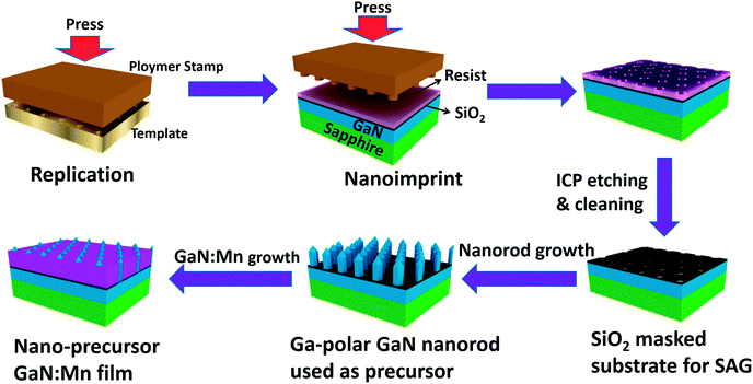
The whole process for the preparation of our sample is shown in Fig. 1. The substrate for growth of the GaN nanorod was a 3 μm layer of c-plane GaN on sapphire capped with a 50 nm SiO2 mask layer. This substrate was prepared by nanoimprinting lithography (NIL) using an Obducat Eitre 3 instrument and inductively coupled plasma (ICP) dry etching using a Samco RIE-200ip etcher. The process of preparing this substrate is similar to that in a previous study by our group.20
The SiO2 mask provided a hexagonally arranged hole pattern with a pitch of 500 nm and a diameter of 200 nm for selective-area growth (SAG)1 of a nanorod. Then, a GaN nanorod array was grown in a Thomas Swan close-coupled showerhead reactor metal-organic chemical vapor deposition (MOCVD) system. The GaN nanorod array was grown to a height of 300 nm via direct nanorod growth with 136 μmol min−1 TMGa, 160 sccm NH3 and 1 sccm SiH4. The substrate temperature was 1068 °C and the reactor pressure was 300 mbar.
Both N-polar (grown directly from sapphire under the SiO2 mask) and Ga-polar nanorod arrays were made and used as precursors for GaN:Mn film. It turned out that only the nanorod array produced via Ga-polar growth could be used as a precursor for the successive growth of GaN:Mn, whereas the nanorod array produced via N-polar growth could not be used. This difference could be explained by the SEM (Nova NanoSEM 430) observations of morphology, as shown in Fig. 2(a) and (b). The nanorod array from Ga-polar growth terminated in a pyramidal top, whereas N-polar growth resulted in a top part having the shape of a truncated pyramid or even a flat top, which means a closed r-plane, in the N-polar nanorod array.21
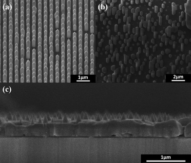 | ||
| Fig. 2 SEM images of (a) Ga-polar GaN nanorod array (45° tilted) (b) N-polar GaN nanorod array (45° tilted) (c) nano-precursor GaN:Mn film (cross-section). | ||
After the Ga-polar nanorod array was made, it was grown into a 450 nm thick GaN:Mn film using 5.64 μmol min−1 TMGa, 0.87 μmol min−1 (MCP)2Mn, 25 sccm NH3 and 1 sccm SiH4, as shown in Fig. 2(c). At this instance, the substrate temperature was 1020 °C and the reactor pressure was 100 mbar. The conventional ferromagnetic GaN:Mn film, which was used for comparison here, was grown directly from c-plane GaN film on sapphire. This was performed at 1060 °C and 100 mbar with a source flow of 11.28 μmol min−1 TMGa, 1.73 μmol min−1 ((MCP)2Mn) and 4.8 slm NH3. The GaN:Mn growth was carried out in a low-pressure horizontal reactor MOCVD system. The Mn concentration of the GaN:Mn film was controlled by varying the ratio of the molar flows of Mn and Ga placed into the reactor, and to incorporate more Mn atoms in the GaN lattice, a high V/III ratio and ultrafast cooling were applied for the growth of GaN:Mn.8 A film with 2.8% Mn content was found to have the most significant ferromagnetic properties among the nano-precursor GaN:Mn films; thus, a conventional GaN:Mn film with 2.8% Mn doping was grown for comparison.
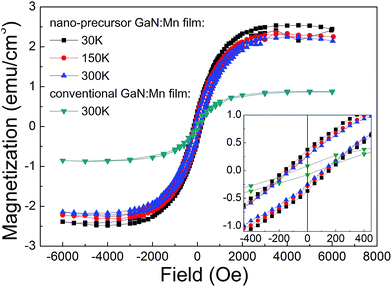
Hysteresis loops were measured to characterise the magnetism of the GaN:Mn films. Because the magnetic signals of most magnetic semiconductors, including GaN:Mn film, are usually weak, very careful operation and measurement as sensitive as possible were used to obtain reliable data.22 Magnetization was measured in the most sensitive RSO mode using a commercial superconducting quantum interference device (SQUID) magnetometer (MPMS XL, Quantum Design) and the result is shown in Fig. 3.
With the bare GaN nanorod array and GaN film, only a diamagnetic background, assigned to the sapphire substrate, could be seen (not shown in Fig. 3). Hysteresis loops of the nano-precursor GaN:Mn film at 30 K, 150 K and 300 K were measured with the external magnetic field parallel to the surface of the film. The result indicated that ferromagnetism occurred above room temperature in the nano-precursor GaN:Mn film, which is similar to the result in conventional GaN:Mn film.8 The slow decrease in saturation magnetization when the temperature increased could be explained by thermal motion of domains.
A comparison with conventional GaN:Mn film shows a 2.5-fold increase from 0.86 emu cm−3 to 2.14 emu cm−3 in saturation magnetization. The inset in Fig. 3 is an enlarged image of the zero-field part of the hysteresis loops, which shows a significant, more than threefold increase, from 0.08 emu cm−3 to 0.26 emu cm−3 in residual magnetization. Moreover, the coercivity increased from 80 Oe to 115 Oe, which is not so significant but much higher than that of their nano counterparts of about 35 Oe.11,13 These results favourably support our nano-precursor hypothesis that a GaN:Mn structure with more point defects might result in magnetic enhancement.
High-resolution X-ray diffraction (HRXRD, Bruker D8) was used to analyse the structure of the samples. In the ω–2θ scan patterns shown in Fig. 4, peaks at 31.1°, 34.5°, 64.8°, 72.9° and 41.8°, corresponding to GaN (100), (002), (103), and (004) faces and sapphire, occur in all the spectra.23 Peaks at 44.2°, 57.8° and 77.5°, which occur only with the nano-precursor GaN:Mn film and bare GaN nanorod array, are produced by the amorphous SiO2 mask layer.24 No additional peaks from Mn-related secondary phases or impurities appear for either Mn-doped GaN films. This result indicates that this type of ferromagnetic GaN:Mn film exists in a single phase, which is similar to the results observed in our previous studies on conventional GaN:Mn films.8
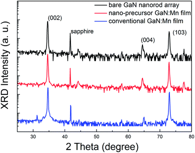 | ||
| Fig. 4 HRXRD ω–2θ scan patterns for bare GaN nanorod array, nano-precursor GaN:Mn film and conventional GaN:Mn film. | ||
Moreover, compared with the bare GaN nanorod array and conventional GaN:Mn film at the same level of Mn doping, rocking curves of the nano-precursor GaN:Mn film were recorded on the (002) and (102) planes. It was found that the full width at half maximum (FWHM) on the (002) plane was 281 arcsec for the nano-precursor GaN:Mn film, 314 arcsec for conventional GaN:Mn film and 270 arcsec for the bare GaN nanorod array. This decrease for the nanostructure and nano-precursor could be understood to be a result of the release of strain in nanorod growth.25 The FWHM on the (102) plane of the nano-precursor GaN:Mn film was 315 arcsec, on the conventional GaN:Mn film was 314 arcsec, and on the bare GaN nanorod array was 309 arcsec. There was no distinct difference among these three. Given that the FWHM on the (002) and (102) planes always relates to screw dislocations and edge dislocations, respectively, the results implied that threading dislocation might not be responsible for the ferromagnetic enhancement.25
We also carried out a preliminary Hall test with the three samples. Ti/Al/Ni/Au (25/120/45/100 nm) electrodes were formed at the four corners of a square with an area of 1 × 1 cm2, followed by 30 s rapid thermal annealing at 830 °C in a N2 atmosphere to form ohmic contact. The measurement was performed with an Accent HL5500 Hall measurement system. Compared with the conventional GaN:Mn film, the nano-precursor GaN:Mn film exhibited lower mobility and a significantly higher carrier concentration. On the one hand, the decrease in mobility could be explained by more defect scattering. On the other hand, the remarkable increase in carrier concentration might be caused by the increase in donor-like point defects. Although further studies, such as deep-level transient spectroscopy (DLTS), needs to be carried out to identify the type of the point defect, these results might imply that there are more point defects in our nano-precursor GaN:Mn film.
Fig. 5 shows the results of Raman scattering (Renishaw confocal Raman microscope) at room temperature. The spectra of the bare GaN nanorod array and conventional GaN:Mn film are also shown for comparison. The peaks at 570 cm−1 and 735 cm−1 are assigned to the EH2 and A1(LO) phonon modes, respectively. Unlike previous studies on room-temperature ferromagnetic GaN:Mn in both films and nanostructures, we did not find any shoulder peak of EH2 at about 588 cm−1, which is always assigned to Mn–N pairs, microprecipitates or clusters in these Raman spectra.13,26–28 Considering the small amount of Mn in both ferromagnetic GaN:Mn films, the amount of Mn or other forms of cluster may not be the most critical factor for ferromagnetism in GaN:Mn materials. This is also incidental evidence of uniform magnetization in the GaN:Mn films.
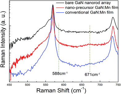 | ||
| Fig. 5 Raman spectra of bare GaN nanorod array, nano-precursor GaN:Mn film and conventional GaN:Mn film. | ||
A small Raman peak at 671 cm−1 occurs for both the conventional GaN:Mn film and nano-precursor GaN:Mn film, but does not appear for the bare GaN nanorod array or conventional GaN film. This difference means that the Raman mode at 671 cm−1 was produced due to Mn doping. This behaviour in the Raman spectrum was also observed when implanting other magnetic ions into GaN and has nothing to do with ionic species.29 This result implies that this ferromagnetism-related Raman mode at 671 cm−1 is assigned, not to the substituting impurities themselves, but to disorder-activated Raman scattering from built-in defects in the intrinsic GaN lattice. In agreement with the results from XRD and Hall measurements, the results implied that the high-temperature ferromagnetism of GaN:Mn film may relate to built-in defects in the intrinsic GaN lattice.
Conclusions
In conclusion, we took advantage of the high surface-to-volume ratio of the nanorod array and pointed out that it has the potential to be a precursor in the production of GaN:Mn with enhanced ferromagnetism via defect control. Herein, GaN:Mn film with 2.8% Mn was grown from a Ga-polar GaN nanorod array as the precursor by MOCVD. As expected, the film exhibited high-temperature ferromagnetism and a significant magnetic enhancement compared with its conventional counterpart. HRXRD and Raman results excluded the possibility of microprecipitates and clusters and assigned the critical reason for ferromagnetism in GaN:Mn to built-in defects in the intrinsic GaN lattice produced by Mn doping. Moreover, the strategy of nano-precursors showed a way to enhance ferromagnetism in DMS and provided a new concept for nanoscale applications in the macroscopic world.Acknowledgements
The study was supported by the National Key Basic Research Special Foundation of China under grants no. 2013CB328705 and 2011CB013101 and the National Natural Science Foundation of China under grants no. 61327801, 61376012, and 61204008.Notes and references
- S. Li and A. Waag, J. Appl. Phys., 2012, 111, 071101 CrossRef.
- M. Tchernycheva, V. Neplokh, H. Zhang, P. Lavenus, L. Rigutti, F. Bayle, F. H. Julien, A. Babichev, G. Jacopin, L. Largeau, R. Ciechonski, G. Vescovi and O. Kryliouk, Nanoscale, 2015, 7, 11692–11701 RSC.
- Y.-T. Lin, T.-W. Yeh, Y. Nakajima and P. D. Dapkus, Adv. Funct. Mater., 2014, 24, 3162–3171 CrossRef CAS.
- I. Žutić, J. Fabian and S. Das Sarma, Rev. Mod. Phys., 2004, 76, 323–410 CrossRef.
- D. D. Awschalom, Y. Ohno, D. K. Young, B. Beschoten, F. Matsukura and H. Ohno, Nature, 1999, 402, 790–792 CrossRef.
- T. Dietl, Science, 2000, 287, 1019–1022 CrossRef CAS PubMed.
- K. Sato and H. Katayama-Yoshida, Jpn. J. Appl. Phys., Part 1, 2001, 40, L485–L487 CAS.
- C. Zhi-Tao, S. Yue-Yong, Y. Zhi-Jian, Z. Yan, Z. Bin, G. Li-Ping, X. Ke, P. Yao-Bao, Z. Han and Z. Guo-Yi, Chin. Phys. Lett., 2006, 23, 1286–1288 CrossRef.
- M. L. Reed, N. A. El-Masry, H. H. Stadelmaier, M. K. Ritums, M. J. Reed, C. A. Parker, J. C. Roberts and S. M. Bedair, Appl. Phys. Lett., 2001, 79, 3473 CrossRef CAS.
- F. Zhang, N. Chen, X. Liu, Z. Liu, S. Yang and C. Chai, J. Cryst. Growth, 2004, 262, 287–289 CrossRef CAS.
- H. J. Choi, H. K. Seong, J. Chang, K. I. Lee, Y. J. Park, J. J. Kim, S. K. Lee, R. He, T. Kuykendall and P. Yang, Adv. Mater., 2005, 17, 1351–1356 CrossRef CAS.
- Y. P. Song, P. W. Wang, X. H. Zhang and D. P. Yu, Phys. B, 2005, 368, 16–24 CrossRef CAS.
- Y. T. Lin, P. V. Wadekar, H. S. Kao, T. H. Chen, H. C. Huang, N. J. Ho, Q. Y. Chen and L. W. Tu, Appl. Phys. Lett., 2014, 104, 062414 CrossRef.
- T. Dietl, Nat. Mater., 2010, 9, 965–974 CrossRef CAS PubMed.
- M. E. Flatté, Nat. Phys., 2011, 7, 285–286 CrossRef.
- B. Hu, B. Y. Man, M. Liu, C. Yang, C. S. Chen, X. G. Gao, S. C. Xu, C. C. Wang and Z. C. Sun, Appl. Phys. A: Mater. Sci. Process., 2012, 108, 409–413 CrossRef CAS.
- G. Thaler, R. Frazier, B. Gila, J. Stapleton, M. Davidson, C. R. Abernathy, S. J. Pearton and C. Segre, Appl. Phys. Lett., 2004, 84, 2578 CrossRef CAS.
- D. J. Keavney, S. H. Cheung, S. T. King, M. Weinert and L. Li, Phys. Rev. Lett., 2005, 95, 257201 CrossRef CAS PubMed.
- X. L. Yang, Z. T. Chen, C. D. Wang, S. Huang, H. Fang, G. Y. Zhang, D. L. Chen and W. S. Yan, J. Phys. D: Appl. Phys., 2008, 41, 125002 CrossRef.
- S. X. Jiang, Z. Z. Chen, X. Z. Jiang, X. X. Fu, S. Jiang, Q. Q. Jiao, T. J. Yu and G. Y. Zhang, CrystEngComm, 2015, 17, 3070–3075 RSC.
- S. F. Li, S. Fuendling, X. Wang, S. Merzsch, M. A. M. Al-Suleiman, J. D. Wei, H. H. Wehmann, A. Waag, W. Bergbauer and M. Strassburg, Cryst. Growth Des., 2011, 11, 1573–1577 CAS.
- M. Sawicki, W. Stefanowicz and A. Ney, Semicond. Sci. Technol., 2011, 26, 064006 CrossRef.
- H. Xiao, R. Liu, H. Ma, Z. Lin, J. Ma, F. Zong and L. Mei, J. Alloys Compd., 2008, 465, 340–343 CrossRef CAS.
- M. B. Boisen, G. V. Gibbs and M. S. T. Bukowinski, Phys. Chem. Miner., 1994, 21, 269 CrossRef CAS.
- W. C. Yang, K. Y. Chen, K.-Y. Cheng, Y. L. Wang, K. C. Hsieh and K. Y. Cheng, J. Cryst. Growth, 2015, 425, 141–144 CrossRef CAS.
- X. Yang, J. Wu, Z. Chen, Y. Pan, Y. Zhang, Z. Yang, T. Yu and G. Zhang, Solid State Commun., 2007, 143, 236–239 CrossRef CAS.
- X. Q. Xiu, R. Zhang, B. B. Li, Z. L. Xie, L. Chen, B. Liu, P. Han, S. L. Gu, Y. Shi and Y. D. Zheng, J. Cryst. Growth, 2006, 292, 212–215 CrossRef CAS.
- M. Asghar, I. Hussain, E. Bustarret, J. Cibert, S. Kuroda, S. Marcet and H. Mariette, J. Cryst. Growth, 2006, 296, 174–178 CrossRef CAS.
- W. Limmer, W. Ritter, R. Sauer, B. Mensching, C. Liu and B. Rauschenbach, Appl. Phys. Lett., 1998, 72, 2589 CrossRef CAS.
| This journal is © The Royal Society of Chemistry 2015 |

