DOI:
10.1039/C5RA15815J
(Paper)
RSC Adv., 2015,
5, 70512-70521
Band edge movement in dye sensitized Sm-doped TiO2 solar cells: a study by variable temperature spectroelectrochemistry
Received
7th August 2015
, Accepted 12th August 2015
First published on 12th August 2015
Abstract
Pure TiO2 and 8 at% Sm-doped TiO2 nanoparticles are prepared via a novel hydrolysis followed by a hydrothermal process at 473 K for 24 h and successfully used in the photoanode of dye sensitized solar cells (DSSCs). The performance of DSSCs based on 8 at% Sm-doped TiO2 is significantly better compared to DSSCs based on undoped TiO2. The Jsc is 14.53 mA cm−2 and η is 6.78%, which is 15% and 5% higher than that of DSSCs based on undoped TiO2, respectively. The results of a variable temperature spectroelectrochemistry study show that the conduction band edge of 8 at% Sm-doped TiO2 shifts positively. The lower conduction band position enhances the driving force of electrons and improves the electron injection efficiency from the lowest unoccupied molecular orbital (LUMO) of the dye to the conduction band (CB) of TiO2, and the narrower band gap expands the response in the visible region and increases the utilization percentage of sunlight. These all contribute to enhancing the performance of cells based on an 8 at% Sm-doped TiO2 photoanode. The as prepared Sm-doped TiO2 material is proven in detail to be a better photoanode material than pure TiO2.
1. Introduction
Dye-sensitized solar cells are promising next-generation alternatives to conventional silicon-based photovoltaic devices because of their great advantages: light weight, low cost and easy processing.1–4 Typically, a DSSC is comprised of a platinum (Pt) counter electrode, a transparent conducting oxide (FTO) electrode, a dye-sensitized nanocrystalline semiconductor film, and an electrolyte containing the I−/I3− redox couple between the two electrodes. The major energy conversion processes in DSSCs can be described as follows. Dye molecules adsorbed on the semiconductor film harvest solar light. Electrons are injected into the CB of the semiconductor film by photo-excited dye molecules. Electrons are then transported toward the FTO front electrode and external circuit. Oxidized dyes are regenerated to a neutral state by I− in the electrolyte and I− is reproduced by the reduction of I3− with electrons which come from the Pt counter electrode.4,5 Among the semiconductor materials used in DSSCs, nanocrystalline anatase TiO2 has been proven to be the best semiconductor electrode material in DSSCs.1,4,6–8 However, there are still many dyes which fail to inject electrons into the conduction band of TiO2 owing to an insufficient electron injection driving force,9 which is defined as the difference between the excited states of the dye (LUMO energy level) and the CB edge of TiO2. The fact that the CB of TiO2 cannot match well with the LUMO of all dyes unavoidably limits the development of DSSCs. Therefore, semiconductor materials with a tunable CB and longer electron lifetime are highly desired for efficient solar cells.
To enlarge the driving force of electron injection for a given dye with an insufficiently high LUMO, tuning of the CB edge of TiO2 positively is a feasible strategy to improve the Jsc performance.10,11 Doping of TiO2 is a commonly adopted method in band edge movement engineering.12–24 However, doping with non-metal elements was limited by the electronegativity and radius of the non-metal dopant,25 and doping with transition metal was suffered from a thermal instability.26 While, in recent years, lanthanides has been widely investigated due to their electronic, optical, and chemical characteristic arising from 4f electrons. Doping just a few rare earth ions into TiO2 can drastically impact on its phase, optical physical and photochemical properties. As reported, Nd-doped TiO2 showed better photocatalytic activity comparing with the blank TiO2 because of its large surface area, fast separation of electron/hole, and narrower band gap.27,28 Eu-doped TiO2 expressed mesoporous structure with bigger surface area and PL responses of characteristic red luminescence at about 618 and 590 nm.29 Sadhu et al.30 found that the flat-band potential of La-doped TiO2 shifted positively and its charge carrier density was also improved. For the material of Er-doped TiO2, upconversion emission was gained through excitation using 978 nm laser beam.31 Sm-doped TiO2 has reported by Park et al.,32 where they used it as a mesoporous catalyst and observed a higher activity due to the large specific surface area and effective separation of the photogenerated electrons from vacancies on account of the Sm specie. However, Sm-doped TiO2 applied in DSSCs and the related mechanism is still not studied in detail.
In this study, we report on the fabrication of 8 at% Sm-doped TiO2 photoanodes for application in DSSCs. It was found that the Sm-doping shifted the CB of TiO2 positively. As a result, Sm-doped TiO2 matches better with the dye N719 that has a sufficiently high LUMO relative to the CB, resulting in significant improvement of Jsc and η. To explicate the effect of Sm doping on CB shifts, we introduce a steady-state variable temperature spectroelectrochemical measurement to determine the conduction band edge in transparent mesoporous semiconducting electrodes that act as working electrodes. Meanwhile, the mechanism of charge transport and recombination, which are related to solar cell performance, has also been studied using intensity modulated photocurrent/photovoltage spectroscopy (IMPS/IMVS) and dark current measurement.
2. Experimental
2.1. Materials and reagents
All of the solvents and chemicals used in this work were of reagent grade without further purification. Sm(NO3)3·6H2O (>99%) was purchased from Rico Chemical Co., Baotou, China. Isopropyl titanate (98%) purchased from J&K CHEMICA Co., Shanghai, China. Propylene carbonate, nitric acid, absolute ethanol, ethyl cellulose, terpineol were purchased from Jinan Henghua Chemical Co., Shandong, China. Acetonitrile, I2, LiI, tert-butylpyridine, lithium perchlorate were purchased from Tianli Chemical Co., Tianjin, China. Ferrocenium, ferrocene (>99%) were purchased from Xilong Chemical Co., Guangdong, China, cis-bis-(isothiocyanato)bis(2,2-bipyridyl-4,4-dicarboxylato)ruthenium(II)bis-tetrabutylammonium (N719) purchased from Solaronix Company, Switzerland. F-doped SnO2-coated glass plate (FTO, 90% transmittance in the visible, 15 Ω cm−2) was purchased from Acros Organics, Belgium, and cleaned by a standard procedure.
2.2. Synthesis of 8 at% Sm-doped TiO2
The TiO2 and 8 at% Sm-doped TiO2 powders were synthesized via a facile hydrothermal method. Typically, 0.4 mL HNO3 was first added into an Erlenmeyer flask containing 1.15 g of Sm(NO3)3·6H2O in 60 mL ultrapure water to adjust the pH value. Then, 10 mL of titanium isopropylate (98%) was added dropwise into above solution under vigorous stirring within 20 minutes. After that, the flask was placed in a water bath of 368 K until the mixture was evaporated to 20 mL transparent sol. The sol was then moved into a 25 mL Teflon-lined stainless steel autoclave and kept in an oven at 473 K for 24 h. After cooled at room temperature, the product was centrifuged and washed with distilled water and ethanol. Then the precipitate was vacuum dried at 373 K, calcined at 773 K for 2 h and cooled to ambient temperature, Sm-doped TiO2 powder was obtained and denoted as 8 at% Sm-doped TiO2. For comparison, undoped TiO2 powder was prepared under the same condition except that Sm(NO3)3·6H2O was not introduced into the reacting system.
2.3. Preparation of film and cell assembly
Pure TiO2 and 8 at% Sm-doped TiO2 paste was prepared according to the literature.33 It was printed onto conductive glass (FTO, 15 Ω sq−1, 90% transmittance in the visible, NSG, Japan) and then dried at 373 K for 5 min. The above process was repeated for six times to make the film thickness was ca.10 μm. The obtained TiO2 film was then sintered at 773 °C for 15 min. It was dyed after immersed in a solution of 0.3 mM N719 in absolute ethanol for 24 h and then washed with ethanol. The sandwich-type solar cell device was assembled by placing a platinum-coated conductive glass as counter electrode on the co-sensitized photoanode, a drop of liquid electrolyte containing 0.5 M LiI, 0.05 M I2, 0.1 M 4-tert-butylpyridine (TBP) was added to fill the void between two electrodes and clipped together as open cells for measurement.
The transparent electrodes of 8 at% Sm-doped TiO2 for spectroelectrochemistry measurement were prepared by doctor-blade route with the paste that was prepared under the same condition with 8 at% Sm-doped TiO2 nanoparticles except that after keeping in an oven at 473 K for 24 h, the obtained product was cooled at room temperature and 0.5–0.6 g Carbowax 20![[thin space (1/6-em)]](https://www.rsc.org/images/entities/char_2009.gif) 000 was added and stirred for more than 3 days. In all cases, the thin films were annealed at 693 K for 30 min. Similarly, the transparent electrodes of undoped TiO2 for spectroelectrochemistry were also prepared.
000 was added and stirred for more than 3 days. In all cases, the thin films were annealed at 693 K for 30 min. Similarly, the transparent electrodes of undoped TiO2 for spectroelectrochemistry were also prepared.
2.4. Characterization
The X-ray powder diffraction (XRD) measurement was obtained on Shimadzu XRD-6000 X-ray Diffraction instrument with Cu-Kα radiation. The X-ray photoelectron spectroscopy (XPS) was measured with an ESCALAB-250 spectrometer (Thermo, America) of the Al Kα source in an ultrahigh vacuum (UHV) at 3.5 × 10⁻⁷ Pa. UV-Vis spectra was performed with UV-2250 spectrophotometer (Shimadzu, Japan). Scanning electron microscopy (SEM) was taken using a Rili SU 8000HSD Series Hitachi New Generation Cold Field Emission SEM and transmission electron microscopy (TEM) was performed using a JEOL JEM-2100 instrument. The PL spectra were measured under the excitation of 350 nm wavelength. The emission can be attributed to the transitions between 500 and 700 nm, which were dispersed by a triple grating monochromator (Spectra Pro-2758, Acton Research Corporation, USA) equipped with a Photo-multiplier (Hamamatsu R928). The Surface Photo-voltage Spectroscopy (SPS) was recorded with assembled instrument by Jilin University, and a 500 W xenon lamp was employed in obtaining monochromatic light through a double-prism monochromator (SBP300, China), and then a lock-in amplifier (SR830, Stanford) served as the signal receiver. IPCE was measured on an EQE/IPCE spectral response system (Newport). The SPS instrument was assembled by Jilin University, in which monochromatic light was obtained by passing light from a 500 W xenon lamp through a double-prism monochromator (SBP300, China), and the signal were collected by a lock-in amplifier (SR830, Stanford). Dark current was recorded by CHI660D Electrochemical Analyzer. Intensity-modulated photocurrent spectroscopy (IMPS) and intensity-modulated photovoltage spectroscopy (IMVS) were carried out on an electrochemical workstation (Zahner Elektrik, Germany) in combination with a white light-emitting diode (WLR-01) and a control system. The intensity-modulated spectra were recorded at room temperature with the light intensity ranged from 30 to 150 mW cm−2, in a modulation frequency ranging from 0.1 to 1000 Hz. The spectroelectrochemical experiments were performed by assembling a potentiostat (Shanghai Chenhua Device Company, China) and a Cary 60 UV-Vis spectrophotometer (Agilent Technologies, America). The current density–voltage (J–V) curves were recorded by Keithley model 2400 digital source meter under AM 1.5 irradiation. The incident light intensity was 100 mW cm−2 calibrated by a standard silicon solar cell. The working areas of the cells were masked to 0.16 cm−2. Based on J–V curve, the fill factor (FF) is defined as: FF = (Jmax × Vmax)/(Jsc × Voc) where Jmax and Vmax are the photocurrent density and photovoltage for maximum power output; Jsc and Voc are the short-circuit photocurrent density and open-circuit photovoltage, respectively, the overall energy conversion efficiency η is defined as: η = (FF × Jsc × Voc)/Pin where Pin is the power of the incident light, Jsc and Voc are also the short-circuit photocurrent density and open-circuit photovoltage, respectively, and FF is the fill factor.
3. Result and discussion
3.1. Structure and morphology characterizations
Fig. 1 shows the XRD results of undoped TiO2 and 8 at% Sm-doped TiO2 powders. The XRD peaks at 2θ = 25.17°, 37.77°, 48.03°, 55.08° and 62.56° in the spectra of undoped TiO2 and 8 at% Sm-doped TiO2 samples are easily identified as a relatively high crystallinity anatase form (JCODS21-1272). However, a diffraction peak at 2θ = 27.40° in the spectra of undoped TiO2, which is easily taken as (110) plane of rutile form was observed. It implies that Sm doping inhibited the phase transformation of TiO2 from anatase to rutile (A–R) significantly. Additionally, it has been found that 8 at% Sm-doped TiO2 showed broader diffraction peaks than undoped TiO2 due to smaller grain sizes.34,35 As determined from the diffraction peak of (101) and Scherrer's equation, the crystalline sizes for undoped TiO2 and 8 at% Sm-doped TiO2 were 14 and 11 nm, respectively. The crystalline size given by the XRD measurements were in agreement with the size of nanoparticles by SEM and TEM analysis (Fig. 2). Furthermore, no impurity or secondary peaks in the XRD patterns were obtained, which indicates that the dopant had inserted the crystal lattice of TiO2.
 |
| | Fig. 1 XRD pattern of pure TiO2 and 8 at% Sm-doped TiO2. | |
 |
| | Fig. 2 SEM and TEM image of (a and c) TiO2 and (b and d) 8 at% Sm-doped TiO2. The insets show the lattice fringes. | |
Also, the SEM morphology in Fig. 2a and b show that the adopted preparation route does not lead to any particular morphology, demonstrating a very low degree of morphological control, and the obtained material consists of aggregated nanoparticles. The TEM morphology of detail inspection of samples at high magnification (Fig. 2c and d) showed the presence of well-crystallized TiO2 nanoparticles with irregular shape and lightly aggregation with the size range of roughly 10–30 nm. The corresponding lattice fringes shown in the insets of Fig. 2c and d were clearly observed, indicating that TiO2 nanoparticles formed with good crystallinity. The interplanar spacing was determined to be 3.51 Å for the undoped and 3.55 Å for the 8 at% doped TiO2 corresponding to the (101) crystal face in the anatase phase. Therefore, it is inferred that the Sm doping played an inhibitory effect in the A–R phase transformation, and favored the formation of anatase with small crystal size in the present synthesis. Although there is no Sm peak observed in XRD patterns of 8 at% Sm-doped TiO2, elemental analysis using X-ray fluorescence (XRF) confirms the presence of Sm in the synthesized 8 at% Sm-doped TiO2 (Table 1).
Table 1 Sm contents in undoped TiO2 and 8 at% Sm-doped TiO2 measured by XRF
| Samples (at% of Sm) |
8 |
| Analyzed Sm content |
| In mass% |
4.94 |
| In at% |
1.53 |
3.2. XPS spectra analysis
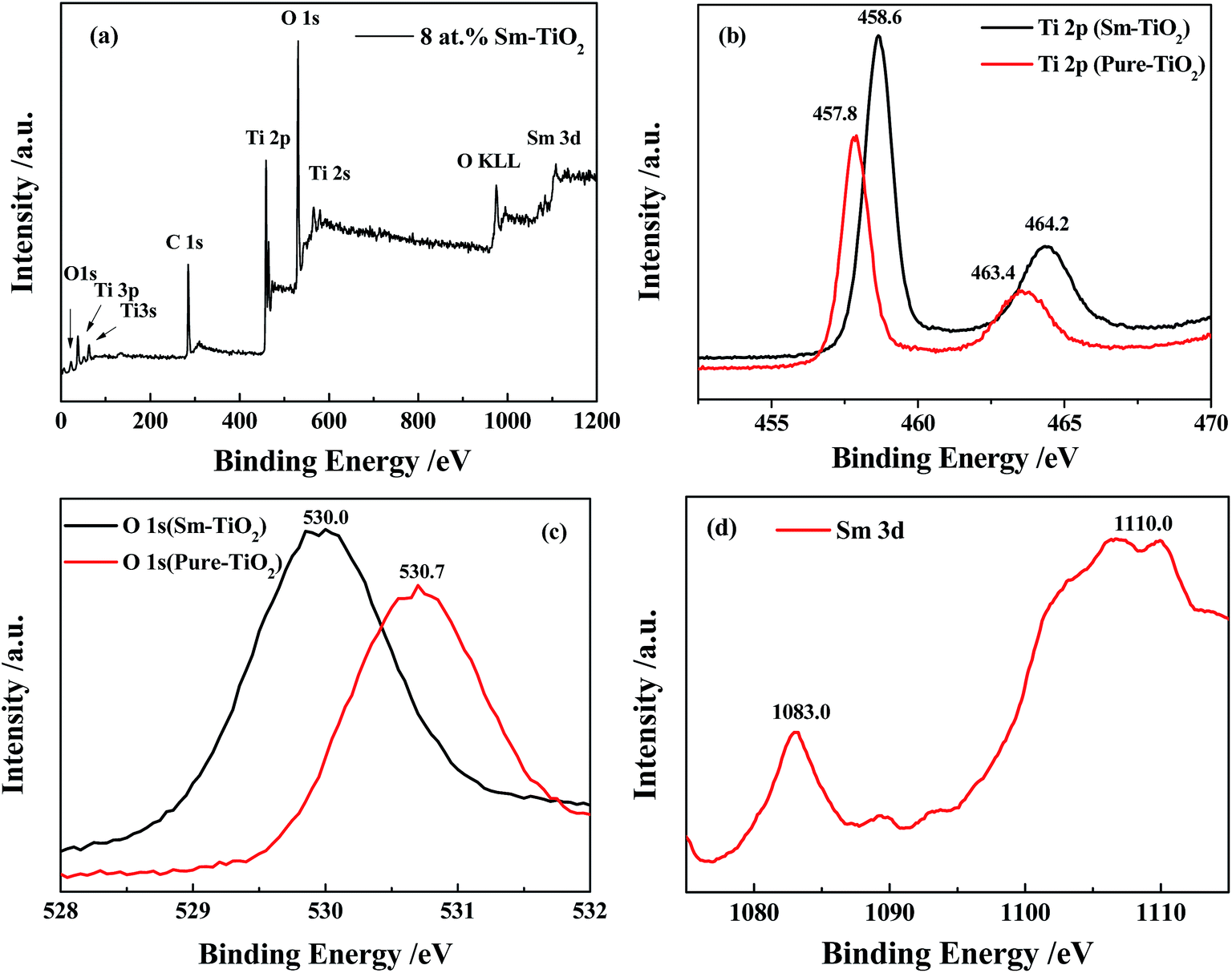
XPS measurements were performed to confirm the existence and bonding nature of various species in 8 at% Sm-doped TiO2. XPS peaks in Fig. 3a indicated that the material contained Ti, O, Sm elements and a trace amount of carbon. Carbon present in sample was considered to be a contamination coming from preparation stages or adsorbed during experiments under vacuum. Compared with pure TiO2, two peaks of doped sample at 458.6 and 464.2 eV, which were ascribed to Ti 2p3/2 and Ti 2p1/2, respectively, shifted toward high binding energy (Fig. 3b). This phenomenon was previously attributed to the change of the local chemical environment of Ti ions influenced by Sm incorporation and the formation of Sm–O–Ti bonds on the surface of TiO2.36 The shift of O 1s binding energy for the Sm-doped TiO2 as compared to the O 1s state of the TiO2 was similar to that observed for the Ti 2p state (Fig. 3c). For Sm 3d spectrum (Fig. 3d), two distinct peaks are observed at 1083.0 eV and 1110.0 eV. This doublet was assigned to Sm 3d5/2 and Sm 3d3/2 levels, respectively, coming from Sm3+ ions.37 These XPS peaks further indicate that Sm was incorporated into the TiO2 lattice.
 |
| | Fig. 3 High-resolution XPS of (a) 8 at% Sm-doped TiO2, (b) Ti 2p, (c) O 1s and (d) Sm 3d. | |
3.3. Optical spectra analysis
The results of XPS and XRD gave evidences that Sm3+ had inserted in TiO2 lattice, and it can be verified by PL spectrum (Fig. 4) at the same time. The PL emission spectrum of 8 at% Sm-doped TiO2 shows the characteristic orange–red luminescence of the trivalent samarium ion upon UV excitation. The emission bands at 587 nm, 613 nm and 664 nm were the electronic transition of 4G5/2–6H5/2, 4G5/2–6H7/2 and 4G5/2–6H9/2 of Sm3+.38 It is worthy to note that these emission bands were all within the absorption wavelength range of N719 dye, it means that N719 could synchronously accept the energy from the incident light and the luminescence of Sm3+, which is better for enhancing the performance of N719 sensitized solar cells.
 |
| | Fig. 4 Emission spectra of 8 at% Sm-doped TiO2 (λex = 350 nm). | |
For the purpose of further investigating the influence of Sm doping process on TiO2 optical absorption, UV-visible absorption spectroscopy was used to study the change of absorption. As shown in Fig. 5a. The broad absorption peak in the wavelength range of 200–400 nm can be attributed to the intrinsic band gap of pure TiO2 (≈3.1 eV), which was generally associated with the electronic excitation of the valence band O 2p electron to the conduction band Ti 3d level. It was easy to observe that the presence of Sm3+ ions made the absorption band edge shift toward long wavelength, namely red shift, which meant the Sm-doped TiO2 powder possessed a narrower band gap that was good for absorbing sunlight.39 Band-gap energy (Eg) of the prepared powders could be calculated from UV-Vis spectroscopy by using the following formula:
| |
 | (1) |
where
λ is the wavelength in nanometers. The inset of
Fig. 5a gives the band-gap energies of pure TiO
2 (≈3.1 eV) and 8 at% Sm-doped TiO
2 (≈2.9 eV). The reduction of the band gap energy of Sm-doped TiO
2 indicated an obvious red shift of light adsorption.
 |
| | Fig. 5 (a) UV-Vis absorption spectra of pure TiO2 and 8 at% Sm-doped TiO2 and (b) surface photovoltage spectroscopy (SPS) of pure TiO2 and 8 at% Sm-doped TiO2. Inset in (a) shows the band gap of pure TiO2 and 8 at% Sm-doped TiO2. | |
Fig. 5b is the surface photovoltage spectroscopy (SPS) of pure TiO2 and 8 at% Sm-doped TiO2. The SPS response which appeared below 400 nm of the two samples arose from the electronic transition from the valence band to the conduction band (O 2p → Ti 3d). Compared with TiO2, the photovoltaic response band of Sm-doped TiO2 was broadened after doping with Sm. Moreover, as shown in the spectra, the response threshold of Sm-doped TiO2 was red-shifted, which resulted in a narrowed band gap. The broadened SPS spectra of 8 at% Sm-doped TiO2 may be attributed to the introduction of impurity sub-bands into the TiO2 when Sm was doped. The SPS spectra further confirmed that doping with Sm narrowed the band gap and red shift the adsorption of TiO2 which is consistent with the results of UV-visible absorption.
3.4. Band edge movement analysis by spectroelectrochemical measurement
As an important class of materials for dye-sensitized solar cells, the conduction and valence band edge positions are considered to be the most important electronic parameters of nanostructure semiconductor TiO2. Information of these energies is crucial in understanding the photophysical and chemical behavior. For instance, the message of band edge positions is extremely important in estimating the driving force for electron injection in DSSCs. Although we found narrower band gap and red shift adsorption of 8 at% Sm-doped TiO2 from optical spectra analysis, still there are some more details and mechanism had not be obtained. However, spectroelectrochemistry is a method which relies on measuring the absorption of band gap energy photons to confirm the concentration of electrons in the conduction band of the transparent semiconducting film and then ascertain the conduction band position in mesoporous nanoparticle based transparent semiconductor films. Therefore, we introduce a steady-state spectroelectrochemical measurement to determine the conduction band edge in transparent mesoporous semiconductor electrodes that act as working electrodes.
Michael Grätzel supposed that the main contribution to the optical absorption at 780 nm comes from the intraband transitions or from free carrier absorption, therefore the absorbance is proportional to the density of electrons in the conduction band.40 Fig. 6 shows the absorbance of pure TiO2 and 8 at% Sm doped TiO2 thin films deposited on an FTO substrate working electrodes measured as a function of applied potential at 780 nm. It is observed that the absorbance follows a rule of exponential functions of applied potential and the absorption of the TiO2 film improved with the increase of the applied negative potential (moving from left to right in the figure). Compared with pure TiO2, 8 at% Sm-doped TiO2 also abided the rule and the film obtained more electrons at the same applied potential (> −0.3 V). What's more, the onset of 8 at% Sm-doped TiO2 was small, which indicates the Fermi level of the 8 at% Sm-doped TiO2 is lower than that of undoped TiO2. The shift of conduction band edge will be accompanied by an equal displacement of quasi-Fermi level relative to the I3−/I− Fermi level. If the electron quasi-Fermi level shifts positively, the conduction band edge also shifts toward the positive direction.41 That means the changed absorbance for 8 at% Sm-doped TiO2 is due to positive shift of conduction band edge and the narrowed band gap which was in consistent with the results of UV-Vis spectroscopy. It is confirmed that after doping with Sm, the bottom of the conduction band of TiO2 was decreased which narrowed band gap and improved driving force of injected electron resulting in increased TiO2 (e−) concentration and absorbance.
 |
| | Fig. 6 Optical absorbance at 780 nm of pure TiO2 and 8 at% Sm-doped TiO2 photoelectrode film. | |
For a deeper research of narrowed band gap of 8 at% Sm-doped TiO2 caused by the conduction band edge movement of TiO2 after doping with Sm, a steady-state spectroelectrochemical measurement with variable temperature was also applied to determine the conduction band edge in transparent mesoporous semiconducting TiO2 working electrodes. The derivatives of TiO2 (e−) concentrations extracted from the spectroelectrochemical data as well as the exponential distribution of the TiO2 (e−) both versus applied potential were plotted as the chemical capacitance as shown in Fig. 7a. The shaded area upon the exponential distribution stands for quantity of charge in the conduction band. And the quantity of this electric charge increased as the temperature raised, which was related to TiO2 (e−) concentration as predicted by eqn (2).
| |
 | (2) |
where
kB is Boltzmann's constant,
T is test temperature,
Ecb is the energy of the conduction band minimum,
EF is the Fermi level energy and
Nc is the effective conduction band density of states.
 |
| | Fig. 7 (a) Chemical capacitance for TiO2 and 8 at% Sm-doped TiO2 thin-film electrodes immersed in the standard electrolyte with 100 mM LiClO4, for TiO2 (e−) as a function of applied potential and (b) histogram of shaded area from (a). | |
It was obvious that at each temperature the quantity of electric charge of Sm-doped TiO2 was larger than pure TiO2 which could be observed clearly from Fig. 7b. This phenomenon can be attributed to the reduction in bottom of the conduction band with Sm modified powder, which gives rise to the quantity of charge in the conduction band.
Fig. 8 presents the averaged values of absorbance for TiO2 and Sm-doped TiO2 at 950 nm with different applied potential and variable temperature. The solid lines in Fig. 8 represent the results of a non-linear least-squares fit to eqn (3) for the data obtained between −0.45 and −0.70 V vs. Ag/AgCl.
| |
 | (3) |
 |
| | Fig. 8 Plot of ln(A) vs. T−1 each line represents a different potential from −0.45 to −0.70 V vs. Ag/AgCl in 50 mV increments from bottom to top. The temperatures correspond to 293, 303, 313, 323 and 333 K. (a) TiO2 and (b) 8 at% Sm-doped TiO2. Error bars represent one standard deviation. The solid lines depict a global fit result to eqn (3) as described in the text. | |
As expected, the absorbance of the films increased with both the increase of applied potential (moving from down to up in the figure) and the increase of the temperature (moving from right to left of the plot). The fit results of Ecb vs. temperature to eqn (3) are listed in Table 2. The results displayed in Table 2 also demonstrate that the absolute value of Ecb increased with the increase of applied potential, and at any given applied potential, Ecb of 8 at% Sm-doped TiO2 is lower than that of undoped TiO2. From this semi-quantitative analysis we obtained the results that doping samarium lowered the conduction band edge of TiO2 which commendably verified the above tests about optical absorption and qualitative analysis of bandgap position.
Table 2 Fit results of absorbance vs. temperature to eqn (3)
| EF (mV vs. Ag/AgCl) |
Ecb/q (mV vs. Ag/AgCl) |
| Sm-doped TiO2 |
TiO2 |
| −450 |
−924.22 |
−801.39 |
| −500 |
−999.84 |
−821.00 |
| −550 |
−1018.14 |
−829.32 |
| −600 |
−1038.79 |
−857.32 |
| −650 |
−1042.97 |
−887.23 |
| −700 |
−1054.03 |
−945.92 |
3.5. Photovoltaic characteristics and performance
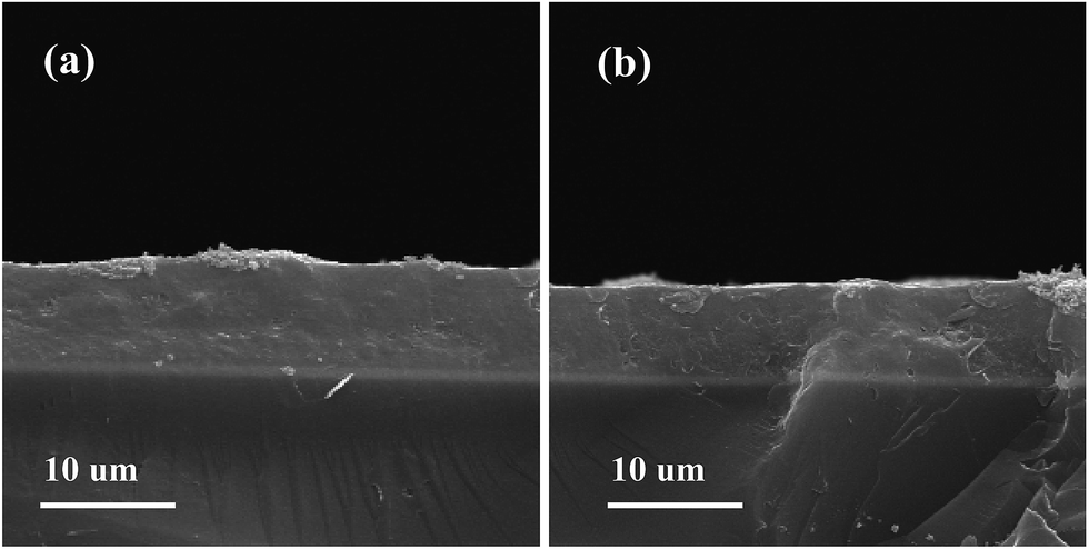
DSSC has attracted extensive interest over the past decades because of energy and environmental issues. TiO2 is widely used for DSSC as an effective photoanode material. For the sake of figuring out the influence of Sm doping on the photoelectric properties of TiO2, two kinds of photoanodes using TiO2 and 8 at% Sm-doped TiO2 powder were prepared and employed into N719 sensitized solar cells. Fig. 9 shows the cross-sectional micrographs of the TiO2 and 8 at% Sm-doped TiO2 photoanodes. From Fig. 9 it is confirmed that the prepared films have firmly adhered onto the FTO substrates and the thickness of the 8 at% Sm-doped TiO2 film is almost the same with that of the undoped TiO2 film. This similar thickness were also obtained by a step srofiler and listed in Table 3.
 |
| | Fig. 9 Cross-sectional micrographs of the (a) TiO2 and (b) 8 at% Sm-doped TiO2 photoanodes. | |
Table 3 Photoelectric properties of DSSC with different photoelectrodes
| Photoanodes |
Thickness (μm) |
Jsc (mA cm−2) |
Voc (V) |
FF |
η (%) |
| 8 at% Sm-doped TiO2 |
10.38 |
14.53 |
0.74 |
0.63 |
6.78 |
| Pure TiO2 |
10.45 |
12.64 |
0.78 |
0.65 |
6.44 |
The current–voltage (J–V) characteristic of the DSSCs devices based on different photoanodes under illumination (AM 1.5 G, 100 mW cm−2) are shown in Fig. 10, and the corresponding cells performance are summarized in Table 3. The DSSC based on 8 at% Sm-doped TiO2 photoanode exhibited a Jsc of 14.53 mA cm−2, a Voc of 0.74 V, and a FF of 0.63 with the energy conversion efficiency (η) of 6.78%, indicating a 15% and 5% increase in Jsc and η than the DSSC based on TiO2 photoanode, which gives a Jsc of 12.64 mA cm−2, a Voc of 0.78 V, and a FF of 0.65 with a η of 6.44%.
 |
| | Fig. 10 Current density versus voltage curves of the DSSCs based on pure TiO2 and 8 at% Sm-doped TiO2 photoelectrodes. | |
The higher η value of DSSC based on 8 at% Sm-doped TiO2 photoanode compared with the DSSC based on TiO2 photoanode, is attributed to the enhanced photovoltaic parameters of Jsc. Obviously, the enhanced Jsc value is ascribed to the enhanced IPCE response of the cell, since they are related by the equation:
| | |
Jsc = ∫eϕph.AM1.5G(λ)dλ
| (4) |
where e is the elementary charge and
ϕph.AM1.5G is the photon flux at AM 1.5 G,
42 the enhanced
Jsc value is ascribed to the enhanced IPCE response of the co-sensitized cell.
Fig. 11a collected the IPCE spectra of the two devices. It is found that doped with Sm could enhance the spectral response of TiO
2 film in the whole visible region and consequently enhance the photocurrent performance. This means the doping of Sm narrows the band gap of TiO
2 which expands the response in the UV-visible region and improves the valid utilization percentage of sunlight. This was confirmed by the UV-Vis absorption spectra of the two photoanodes (
Fig. 11b). Based on the IPCE and the absorption spectra, it could be conclude that the cell's higher
Jsc in the case of 8 at% Sm-doped TiO
2 is ascribed to the improved utilization percentage of sunlight.
 |
| | Fig. 11 (a) IPCE spectra of DSSCs based on TiO2 and Sm-doped TiO2 photoanodes and (b) UV-Vis spectra of TiO2 and Sm-doped TiO2 photoanodes. | |
However, the FF and Voc of the DSSC based on 8 at% Sm-doped TiO2 photoanode decreased to 0.63 and 0.74 V, respectively. As discussed above, the movement of conduction band edge potential (Ecb) of Sm-doped TiO2 decreases the energy gap between the Fermi level (EF) and the potential of the I−/I3− redox species (Ered) in the electrolyte, resulting in the phenomenon that the Voc of Sm-doped TiO2-based DSSC decreased. In this study, the Voc value can be described as eqn (5):
Assuming that Ered of I−/I3− in the electrolyte does not change with the dopant, it is anticipative that the Voc relies on the EF, which is related to the Ecb position. So it is definite that the lower conduction band edge of TiO2 results in less Voc.41
After samarium doping, the conduction band edge moves to lower position. This indicates the driving force for electron injection increases, which enhances the electron injection efficiency from the LUMO of the dye to the conduction band of TiO2. Meanwhile, after samarium doping, the recombination between injected electrons and oxide dye cation and/or the oxidized form of the redox shuttle decreased. These were also benefit for improving the performance of DSSC based on 8 at% Sm-doped TiO2 photoanode. The reduction of recombination could be verified by dark current measurement of different DSSCs.
Dark current measurement of DSSCs is considered as a qualitative technique to describe the extent of the back electron transfer.43,44 It could provide useful information regarding the back electron transfer process by making a comparison of dark current between the investigated cells. Therefore, dark current of cells based on undoped TiO2 and 8 at% Sm-doped TiO2 were measured and are shown in Fig. 12. By comparing the curves in Fig. 12, it is found that the onset of the dark current for DSSC based on pure TiO2 is at a bias about +0.35 V, and then the dark current increase remarkably with the increase of potential. In contrast, for the DSSC based on 8 at% Sm-doped TiO2, the onset potential shifted to about +0.40 V; furthermore, the dark current of the DSSC based on 8 at% Sm-doped TiO2 increased much slower than that of DSSC based on pure TiO2 when potential was greater than +0.40 V. In other words, under the same potential bias, when the potential was ≥0.40 V, the dark current for the DSSCs based on 8 at% Sm-doped TiO2 was noticeably smaller than that for the DSSC based on pure TiO2. The increase of the onset potential and the reduction of the dark current demonstrated that 8 at% Sm-doped TiO2 successfully suppress the electron back reaction with I3− in the electrolyte.
 |
| | Fig. 12 Dark current of the DSSCs based on different photoelectrodes. | |
3.6. IMPS and IMVS measurements for DSSCs
In order to further investigate the electron-transfer and charge-recombination processes beside band edge movement in the DSSCs based on Sm-doped TiO2 and pure TiO2, IMPS and IMVS of devices based on different photoelectrodes were measured. Electron diffusion length (Ln), and electron collection efficiency (ηcc) are very important factors for the performance of DSSCs. They can reflect the competition between the transport and recombination of electrons, and can be derived from IMVS–IMPS measurements according to the following equations:where Dn is the diffusion coefficient, which can be obtained by the eqn (6), τr is the electron lifetime which can be calculated by the characteristic frequency at the minimum of the imaginary component with the IMVS result, τt is the electron transport time which can be computed by the characteristic frequency at the minimum of the imaginary component of the IMPS result, and d is the thickness of the photoanode in IMPS and IMVS analysis.45
Fig. 13a and b show the electron diffusion length (Ln), and electron collection efficiency (ηcc) of the DSSCs based on 8 at% Sm-doped TiO2 and pure TiO2 photoanodes, plotted as a function of the incident light intensity. Fig. 13a shows that the Ln values of the Sm-doped TiO2 based DSSC were greater than those of pure TiO2. Furthermore, the ηcc values of the Sm-doped TiO2-based cell were greater than those of the pure TiO2-based cell (Fig. 13b). The improvement of these parameters in the Sm-doped TiO2 nanostructure can be also attributed to its band edge moment. Lower movement of conduction band bottom provides stronger driving force of electrons injection and more effectively suppress the charge recombination. Thereby, the τr value of Sm-doped TiO2 is larger and the τt value is smaller than those of pure TiO2. On the other hand, the movement of conduction band edge in 8 at% Sm-doped TiO2 made the bad gap become smaller and improved the utilization rate for sunlight. Meanwhile, 8 at% Sm-doped TiO2 can emit orange–red luminescence under the irradiation of ultraviolet light which improves the absorption of light for dye and then improved the Ln and ηcc values.
 |
| | Fig. 13 (a) electron diffusion length and (b) charge collection efficiency of pure TiO2 and 8 at% Sm-doped TiO2. | |
4. Conclusions
8 at% Sm-doped TiO2 was produced by an easy hydrothermal route and was employed into ruthenium dye N719 sensitized solar cells. It was found that after doping with Sm, the conduction band edge moves to lower position. Lower movement of conduction band edge provides stronger driving force for electrons injection from the LUMO of the dye to the conduction band of TiO2 and more effectively suppress the charge recombination between injected electrons and oxide dye cation and/or the oxidized form of the redox shuttle. The movement of conduction band edge in 8 at% Sm-doped TiO2 made the bad gap become smaller and improved the valid utilization percentage of sunlight. Meanwhile, 8 at% Sm-doped TiO2 can emit orange–red luminescence under the irradiation of ultraviolet light which improves the absorption light for dye N719. These were all benefit for improving the performance of DSSCs. Therefore, the DSSC based on 8 at% Sm-doped TiO2 exhibited an excellent performance with a Jsc of 14.53 mA cm−2, a Voc of 0.74 V, and a FF of 0.63 with the energy conversion efficiency (η) of 6.78%, indicating a 15% and 5% increase in Jsc and η than the DSSC based on pure TiO2 photoanode.
Acknowledgements
This work was supported by National Natural Science Foundation of China (Grant 21171044 and 21371040), the National Key Basic Research Program of China (973 Program, 2013CB632900), and the Fundamental Research Funds for the Central Universities (Grant HIT. IBRSEM. A. 201409), also Program for Innovation Research of Science in Harbin Institute of Technology (PIRS of HIT A201416 and B201414).
Notes and references
- B. O'Regan and M. Grätzel, Nature, 1991, 353, 737–740 CrossRef PubMed.
- M. Grätzel, Acc. Chem. Res., 2009, 42, 1788–1798 CrossRef PubMed.
- S. K. Balasingam, M. Lee, M. G. Kang and Y. Jun, Chem. Commun., 2013, 49, 1417–1487 Search PubMed.
- A. Hagfeldt, G. Boschloo, L. C. Sun, L. Kloo and H. Pettersson, Chem. Rev., 2010, 110, 6595–6663 CrossRef CAS PubMed.
- S. Ardo and G. J. Meyer, Chem. Soc. Rev., 2009, 38, 115–164 RSC.
- M. Law, L. E. Greene, J. C. Johnson, R. Saykally and P. Yang, Nat. Mater., 2005, 4, 455–459 CrossRef CAS PubMed.
- Q. Huang, G. Zhou, L. Fang, L. Hu and Z. S. Wang, Energy Environ. Sci., 2011, 4, 2145–2151 CAS.
- T. Chen, S. Wang, Z. Yang, Q. Feng, X. Sun, L. Li, Z. S. Wang and H. Peng, Angew. Chem., Int. Ed., 2011, 50, 1815–1819 CrossRef CAS PubMed.
- Z. S. Wang, Y. Cui, Y. Dan-oh, C. Kasada, A. Shinpo and K. Hara, J. Phys. Chem. C, 2008, 112, 17011–17017 CAS.
- X. M. Ren, Q. Y. Feng, G. Zhou, C. H. Huang and Z. S. Wang, J. Phys. Chem. C, 2010, 114, 7190–7195 CAS.
- K. P. Wang and H. Teng, Phys. Chem. Chem. Phys., 2009, 11, 9489–9496 RSC.
- U. G. Akpan and B. H. Hameed, Appl. Catal., A, 2010, 375, 1–11 CrossRef CAS PubMed.
- W. Li, Z. X. Wu, J. X. Wang, A. A. Elzatahry and D. Y. Zhao, Chem. Mater., 2014, 26, 287–298 CrossRef CAS.
- M. H. Li, S. J. Zhang, Y. Peng, L. Lv and B. C. Pan, RSC Adv., 2015, 5, 7363–7369 RSC.
- Y. Xia, Y. S. Jiang, F. F. Li, M. S. Xia, B. Xue and Y. J. Li, Appl. Surf. Sci., 2014, 289, 306–315 CrossRef CAS PubMed.
- J. M. Liu, Q. C. Zhang, J. C. Yang, H. Y. Ma, M. O. Tade, S. B. Wang and J. Liu, Chem. Commun., 2014, 50, 13971–13974 RSC.
- W. Q. Fang, Z. Y. Huo, P. R. Liu, X. L. Wang, M. Zhang, Y. Jia, H. M. Zhang, H. J. Zhao, H. G. Yang and X. D. Yao, Chem.–Eur. J., 2014, 20, 11439–11444 CrossRef CAS PubMed.
- S. Sood, A. Umar, S. K. Mehta and S. K. Kansal, J. Colloid Interface Sci., 2015, 450, 213–223 CrossRef CAS PubMed.
- C. Z. Wang, Z. Chen, H. B. Jin, C. B. Cao, J. B. Li and Z. T. Mi, J. Mater. Chem. A, 2014, 2, 17820–17827 CAS.
- A. Q. Wang and H. W. Jing, Dalton Trans., 2014, 1011–1018 RSC.
- B. Y. Ao, Z. J. Zhang, T. Tang and Y. P. Zhao, Solid State Commun., 2015, 204, 23–27 CrossRef CAS PubMed.
- S. G. Kim, M. J. Ju, I. T. Choi, W. S. Choi, H. J. Choi, J. B. Baekb and H. K. Kim, RSC Adv., 2013, 3, 16380–16386 RSC.
- F. L. Zhang, Z. Q. Cheng, L. J. Kang, L. Y. Cui, W. Liu, X. J. Xu, G. H. Hou and H. J. Yang, RSC Adv., 2015, 5, 32088–32091 RSC.
- T. N. Ravishankar, T. Ramakrishnappa, H. Nagabhushana, V. S. Souza, J. Dupontc and G. Nagaraju, New J. Chem., 2015, 39, 1421–1429 RSC.
- R. Y. Zhang, A. A. Elzatahry, S. S. Al-Deyab and D. Y. Zhao, Nano Today, 2012, 7, 344–366 CrossRef CAS PubMed.
- Y. C. Nah, I. Paramasivam and P. Schmuki, ChemPhysChem, 2010, 11, 2698–2713 CrossRef CAS PubMed.
- A. Bokare, M. Pai and A. A. Athawale, J. Sol. Energy, 2013, 91, 111–119 CrossRef CAS PubMed.
- J. M. Du, H. J. Chen, H. Yang, R. R. Sang, Y. T. Qian, Y. X. Li, G. G. Zhu, Y. J. Mao, W. He and D. J. Kang, Microporous Mesoporous Mater., 2013, 182, 87–94 CrossRef CAS PubMed.
- C. Leostean, M. Stefan, O. Pana, A. I. Cadis, R. C. Suciu, T. D. Silipas and E. Gautron, J. Alloys Compd., 2013, 575, 29–39 CrossRef CAS PubMed.
- S. Sadhu and P. Poddar, RSC Adv., 2013, 3, 10363–10369 RSC.
- J. Reszczýnska, T. Grzyb, J. W. Sobczak, W. Lisowski, M. Gazda, B. Ohtani and A. Zaleska, Appl. Catal., B, 2015, 163, 40–49 CrossRef PubMed.
- D. J. Park, T. Sekino, S. Tsukuda, A. Hayashi, T. Kusunose and S. I. Tanaka, J. Solid State Chem., 2011, 184, 2695–2700 CrossRef CAS PubMed.
- P. Y. Reddy, L. Giribabu, C. Lyness, H. J. Snaith, C. Vijaykumar, M. Chandrasekharam, M. Lakshmikantam, J. H. Yum, K. Kalyanasundaram, M. Grätzel and M. K. Nazeeruddin, Angew. Chem., Int. Ed., 2007, 46, 373–376 CrossRef CAS PubMed.
- J. T. Tang, X. M. Chen, Y. Liu, W. Gong, Z. S. Peng, T. J. Cai, L. J. Luo and Q. Deng, Solid State Sci., 2013, 15, 129–136 CrossRef CAS PubMed.
- V. Stengl, S. Bakardjieva and N. Murafa, Mater. Chem. Phys., 2009, 114, 217–226 CrossRef CAS PubMed.
- Y. C. Cao, Z. Y. Zhao, J. Yi, C. S. Ma, D. C. Zhou, R. F. Wang, C. Li and J. B. Qiu, J. Alloys Compd., 2013, 554, 12–20 CrossRef CAS PubMed.
- S. Asal, M. Saif, H. Hafez, S. Mozia, A. Heciak, D. Moszyński and M. S. A. Abdel-Mottaleb, Int. J. Hydrogen Energy, 2011, 36, 6529–6537 CrossRef CAS PubMed.
- M. Ishii, B. Towlson, N. Poolton, S. Harako, X. W. Zhao, S. J. Komuro and B. Hamilton, J. Appl. Phys., 2012, 111, 1–14 Search PubMed.
- M. Saif and M. S. A. Abdel-Mottaleb, Inorg. Chim. Acta, 2007, 360, 2863–2874 CrossRef CAS PubMed.
- G. Rothenberger, D. Fitzmaurice and M. Grätzel, J. Phys. Chem., 1992, 96, 5983–5986 CrossRef CAS.
- J. Yu, Y. L. Yang, R. Q. Fan, L. Li and X. Y. Li, J. Phys. Chem. C, 2014, 118, 8795–8802 CAS.
- G. D. Sharma, G. E. Zervaki, P. A. Angaridis, A. Vatikioti, K. S. V. Gupta, T. Gayathri, P. Nagarjuna, S. P. Singh, M. Chandrasekharam, A. Banthiya, K. Bhanuprakash, A. Petrou and A. G. Coutsolelos, Org. Electron., 2014, 15, 1324–1337 CrossRef CAS PubMed.
- A. Zaban, A. Meier and B. A. Gregg, J. Phys. Chem. B, 1997, 101, 7985–7990 CrossRef CAS.
- S. Ito, P. Liska, P. Comte, R. L. Charvet, P. Pechy, U. Bach, L. Schmidt-Mende, S. M. Zakeeruddin, A. Kay, M. K. Nazeeruddin and M. Grätzel, Chem. Commun., 2005, 4351–4353 RSC.
- X. H. Miao, K. Pan, Y. P. Liao, W. Zhou, Q. J. Pan, G. H. Tian and G. F. Wang, J. Mater. Chem. A, 2013, 1, 9853–9861 CAS.
|
| This journal is © The Royal Society of Chemistry 2015 |
Click here to see how this site uses Cookies. View our privacy policy here.