
 Open Access Article
 This Open Access Article is licensed under a Creative Commons Attribution-Non Commercial 3.0 Unported Licence
Effect of UV light-induced nitrogen doping on the field effect transistor characteristics of graphene†
Gaku
Imamura
*ab and
Koichiro
Saiki
b
aWorld Premier International (WPI) Research Center, International Center for Materials Nanoarchitectonics (MANA), National Institute for Materials Science (NIMS), 1-1 Namiki, Tsukuba, Ibaraki 305-0044, Japan. E-mail: IMAMURA.Gaku@nims.go.jp; Fax: +81-29-860-4706; Tel: +81-29-851-3354 ext. 4186
bDepartment of Complexity Science and Engineering, Graduate School of Frontier Sciences, The University of Tokyo, Kashiwanoha 5-1-5, Kashiwa, Chiba 277-8561, Japan
First published on 12th August 2015
Abstract
The effect of nitrogen doping on graphene was characterized without exposing the prepared specimen to the atmosphere. Nitrogen doping was done via a photochemical process at room temperature, in which graphene on SiO2/Si was irradiated by UV light in ammonia. Field effect transistor measurements revealed that the UV-irradiation of graphene in NH3 causes electron doping of ∼1012 cm−2 (∼0.01%) as a result of N-doping, which can be controlled by changing the irradiation time. Comparing the transfer characteristics and the Raman spectra, we discuss the structure of the graphene functionalized via photochemical reactions, and the corresponding electronic structure.
Introduction
Graphene, a one atom thick sheet of sp2 carbon atoms arranged in a honeycomb configuration, has been intensively studied as a novel 2D material in recent years. Its prominent mechanical, electronic and chemical properties make graphene a key material for next-generation technologies.1,2 Doping graphene with heteroatoms is one of the most promising methods for modifying its properties.3 It is reported that nitrogen (N) doping gives rise to the evolution of a band gap.4,5 Opening the band gap leads to a high on/off ratio, which is essential for application to electronic devices. Another interesting phenomenon evoked by N-doping is the catalytic activity for oxygen reduction reaction,6 the cathode reaction of fuel cells. Carbon alloy catalysts (CACs), the assembly of N-doped graphene, can be seen as an inexpensive alternative to platinum.7,8 With regard to CACs, increased conductivity by electron doping as a result of N-doping is important rather than emergence of a band gap. Despite the many studies on the synthesis of N-doped graphene,9–17 controlling the doping level is still a big challenge. One of the major reasons is the trade-off relationship between the degree of graphenization and the N-doping amount; the former requires a high growth temperature, while the latter decreases rapidly with temperature.13–17 To overcome such a dilemma, a N-doping method effective still at room temperature is required. In addition, a direct N-doping method to graphene that can control the doping level has been highly anticipated. Most of past studies using chemical vapour deposition (CVD) needed a transfer process for characterization, which made it difficult to deduce the intrinsic nature of doping due to the inevitable subsidiary effect.In our previous study, we succeeded in fabricating N-doped graphene by exposing the graphene to NH3 atmosphere under UV light irradiation.18 This method enables us to characterize the electrical properties before and after N-doping in situ. In the present study, we have observed a shift of the charge neutrality point (CNP) to the negative direction after the UV-irradiation in NH3, which indicates electron doping to graphene. The doping levels can be controlled in the range of 1012 to 1013 cm−2 by varying the irradiation time. On the basis of transport measurements and Raman spectroscopy, we discuss the possible structure for the N-doped graphene.
Experimental
There are several methods to fabricate graphene such as mechanical exfoliation of graphite, epitaxial growth on SiC, reduction of graphene oxide, and CVD process including solid carbon sources.19–25 To ensure the quality and uniformity of graphene on SiO2, we purchased graphenes on SiO2 (285 nm)/Si from Graphene Laboratories Inc., which were fabricated via CVD process. The specimens were taken from the same lot. Fig. 1 shows a schematic illustration of the experimental setup. To fabricate a field effect transistor (FET) structure, 20 nm-thick gold pads were deposited onto the graphene as source and drain electrodes. After wiring the electrodes to vacuum feedthroughs, the chamber was evacuated to ∼10−6 Pa. Electrical measurements and UV-irradiation were performed in the vacuum chamber. Prior to electrical measurements, the graphene was annealed in a vacuum at 160 °C for several hours, which removed adsorbed molecules and contaminants. Ammonia was introduced into the chamber via a variable leak valve. A deuterium lamp (L2D2, 30 W, Hamamatsu Photonics K.K.) was used for UV-irradiation. The peak emission wavelength of the lamp is around 150–200 nm, and the effective power density is estimated to ∼0.01 mW cm−2. Raman spectroscopy was performed in air with excitation wavelength of 532 nm. | ||
| Fig. 1 Schematic illustration of the experimental setup. | ||
Results and discussion
Fig. 2a shows the FET characteristics of the graphene before and after UV-irradiation in NH3. Typical transfer characteristics of pristine graphene could be observed before the UV-irradiation;26 CNP was located at around 0 V, and the curve exhibited a small hysteresis. The carrier mobility of the graphene was 1100 cm2 (V−1 s−1) and 2300 cm2 (V−1 s−1) for electron and hole transport, respectively. After the FET measurement, the graphene was UV-irradiated under 10 Pa of NH3 for 1 h at RT. The evolution of a hysteresis and the decrease of mobility was observed after the UV-irradiation (Fig. 2a). For the forward sweep (from a negative to a positive gate voltage), the electron mobility (µe) and hole mobility (µh) decreased to 720 cm2 (V−1 s−1) and 1200 cm2 (V−1 s−1), respectively. µe and µh for the backward sweep (from a positive to a negative gate voltage) were 790 cm2 (V−1 s−1) and 940 cm2 (V−1 s−1), respectively. The evolution of a hysteresis and the decrease of mobility were explained by the formation of sp3-like bonds at the graphene/SiO2 interface as described in ref. 27. Our previous study showed that UV-irradiation in a vacuum triggers a photochemical reaction at the graphene/SiO2 interface, which gives rise to the decrease in mobility and the hysteresis that was counter clockwise on the negative side and clockwise on the positive side. Another noticeable change in FET characteristics after the UV-irradiation in NH3 was a shift in the CNP to the negative direction. The CNP is shifted by −16 V after the UV-irradiation in NH3, while UV-irradiation in a vacuum does not shift the CNP.27 Hence, it is implied that the CNP is shifted to the negative direction as a result of N-doping, by which nitrogen atoms are incorporated into the graphene lattice. Incorporation of N atoms by UV irradiation in ammonia was confirmed by X-ray photoelectron spectroscopy in our previous study.18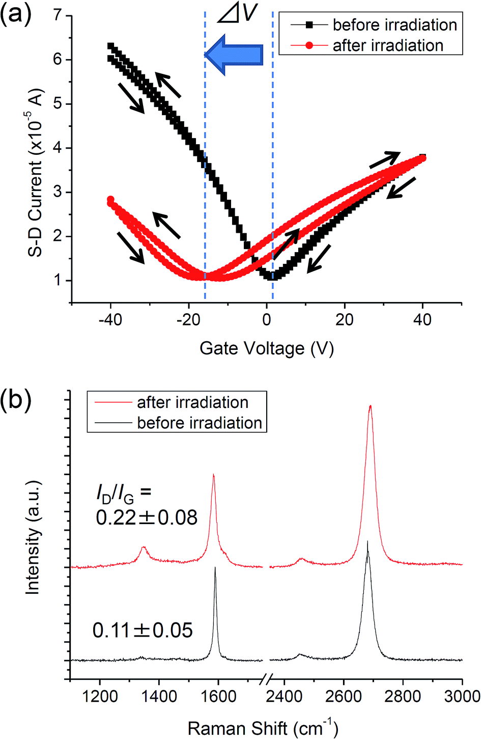 | ||
| Fig. 2 (a) Transfer characteristics of graphene before and after the UV-irradiation in NH3. (b) Raman spectra of graphene before and after the UV-irradiation in NH3. | ||
Fig. 2b shows the Raman spectra of the graphene before and after the UV-irradiation in NH3. Three inherent peaks for graphene are seen for both spectra: the G band (∼1585 cm−1), the D band (∼1350 cm−1), and the 2D band (∼2700 cm−1).28 The D band originating from the A1g vibrational mode of hexagonal sp2 carbon network becomes Raman active by defects. Therefore, the intensity ratio of the D band to the G band (ID/IG) is a good indicator for evaluating the density of defects.29,30 While the pristine graphene showed small ID/IG (0.11 ± 0.05), the graphene UV-irradiated in NH3 exhibited higher ID/IG (0.22 ± 0.08). Thus defects were introduced into the graphene lattice by the UV-irradiation in NH3. As the sharp symmetric 2D band was not substantially changed after irradiation, the structure of monolayer graphene remained.31 The widening of the 2D band reflects the defect formation in graphene.32,33
To investigate the dependence on the irradiation time, graphene was UV-irradiated in 10 Pa of NH3 for longer times (2 h and 4 h). The shift in CNP (ΔVCNP) was plotted as a function of irradiation time in Fig. 3a. ΔVCNP is almost proportional to the irradiation time. We estimate the doped electron density (ne) from ΔVCNP according to the capacitor relationship: ne = CoxΔVCNP/e, where Cox and e are the capacitance of SiO2 per area and the elementary charge, respectively. ne for the graphene UV-irradiated in NH3 for 1 h, 2 h, and 4 h is estimated to 1.3 × 1012 cm−2, 3.4 × 1012 cm−2, 6.1 × 1012 cm−2, respectively. Considered that the atomic number density of graphene is 3.8 × 1015 cm−2, the corresponding doping level for the graphene UV-irradiated in NH3 for 1 h, 2 h, and 4 h is 0.034%, 0.089%, and 0.16%, respectively. Thus the electron density of graphene can be controlled in the range of 1012 to 1013 cm−2 (0.01%) by the UV-irradiation in NH3. With regard to carrier mobility, the changes in electron and hole mobility (µe and µh, respectively) are summarised in Table 1.
 | ||
| Fig. 3 (a) ΔVCNP as a function of irradiation time. (b) Raman ID/IG as a function of irradiation time. | ||
| Irradiation time | µ e (cm2 V−1 s−1) | µ h (cm2 V−1 s−1) | V CNP (V) | |
|---|---|---|---|---|
| a Mobility cannot be calculated because gate voltage more negative than 80 V could not be applied to prevent dielectric breakdown. | ||||
| 1 h | Before | 1000 | 2300 | 1 |
| After (− → +) | 720 | 1200 | −18 | |
| After (+ → −) | 790 | 940 | −12 | |
| 2 h | Before | 1500 | 1800 | 2 |
| After (− → +) | 710 | 790 | −41 | |
| After (+ → −) | 770 | 640 | −38 | |
| 4 h | Before | 1200 | 1600 | 3 |
| After (− → +) | 510 | —a | −73 | |
| After (+ → −) | 500 | —a | −70 | |
To elucidate the relation between the N-doping and the formation of sp3-like bonds by the UV-irradiation, we compared the results with the data from the graphene UV-irradiated in a vacuum.27 With regard to the FET characteristics, the CNP is shifted to the negative side after UV-irradiation in NH3, while the CNP stays at around 0 V for the graphene UV-irradiated in a vacuum (Fig. 3a). The difference between NH3 and vacuum can also be seen in the change of Raman spectra as shown in Fig. 3b. While the ID/IG monotonically increased with irradiation time for both conditions, the degree of increase is larger for the UV-irradiation in NH3 than that in a vacuum. This higher ID/IG implies that graphene is damaged by N-doping as well as the formation of sp3-like bonds caused by UV-light.
The effect of adsorption of ammonia on graphene was also studied by exposing the graphene on SiO2/Si to 10 Pa of NH3 for 1 h without UV-light. Fig. 4a shows the FET characteristics before and after the exposure. No noticeable change can be observed after the UV-irradiation without a small shift of CNP to the negative direction. Such small negative shift after the exposure to NH3 has also been reported by Romero et al., which is considered to be caused by displacement chemical reactions in the graphene/SiO2 interface.34 The Raman spectra also showed no changes at all (Fig. 4b).
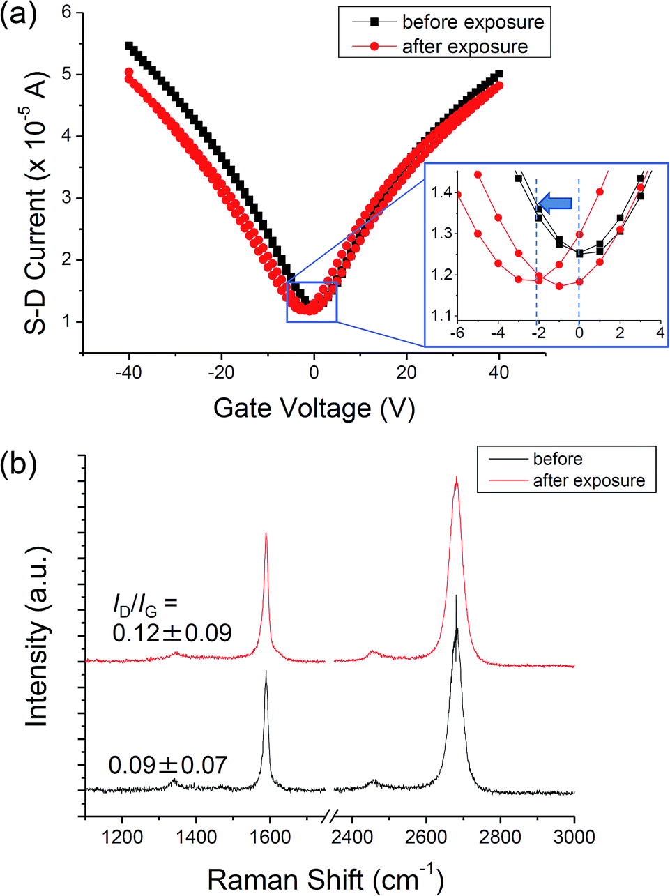 | ||
| Fig. 4 (a) Transfer characteristics of graphene before and after exposure to NH3. (Inset) Enlarged transfer characteristics at around the Dirac point. (b) Raman spectra of graphene before and after exposure to NH3. | ||
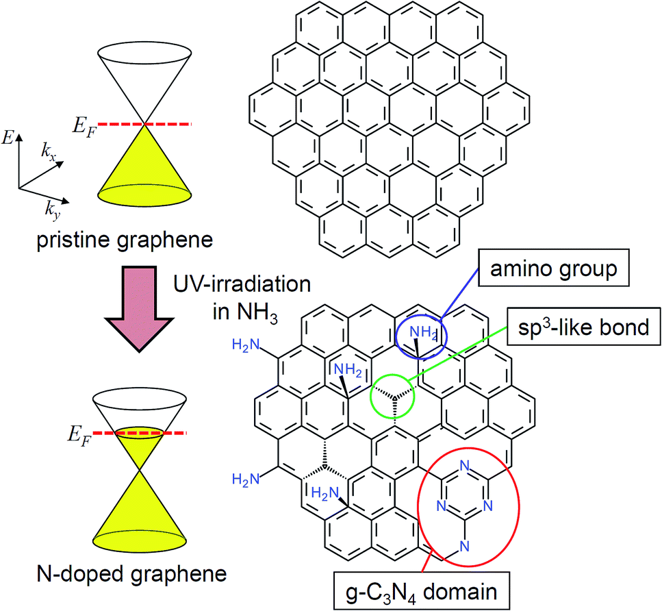
On the basis of the experimental results, we propose a possible structure of N-doped graphene together with the electronic structure in Fig. 5. Before the UV-irradiation in NH3, the Fermi level was located at the Dirac point judging from the VCNP of around 0 V (Fig. 2a). The shift of the CNP after the UV-irradiation in NH3 indicated that electrons were doped into graphene, and the Fermi level was shifted to higher energy. It is known that UV light induces a photodissociation reaction of NH3 molecules described as
| NH3 → NH2 + H, |
 | ||
| Fig. 5 Schematic illustration of N-doped graphene and the corresponding electronic structure. | ||
The density of defects (σd) can be estimated from the Raman ID/IG. According to the Tuinstra–Koenig relation, the average crystalline size (La) is described as La = C/(ID/IG), where C is a constant depending on the excitation wavelength (C = 19.2 for 532 nm).29,30,38 As La is the average distance between the defects, σd is written as σd = 1/La2 = (ID/IG)2/C2. Note that any structural disorders including vacancies, sp3 carbon structures, and doped impurities contribute to σd in this estimation. As ID/IG was 0.22 ± 0.08 for the graphene UV-irradiated in NH3 for 1 h, σd is estimated to be 1.26 × 1010 cm−2, which is approximately 1/100 of the doped electron density (ne) estimated from the shift of the CNP (1.3 × 1012 cm−2). This significant deviation implies that defect formation including N-doping occurs rather locally. The estimation of σd assumes randomly distributed defects in graphene. Therefore σd is likely to be underestimated if defects are locally formed. It is highly plausible that defects are localized in some regions of graphene. Formation of g-C3N4 domains is one of such examples. As we have discussed in the previous study, X-ray photoelectron spectroscopy implies that g-C3N4 domains are formed in the graphene lattice.18 Another case is that defects such as amino groups or sp3-like bond are localized at the periphery of graphene grains. As it is known that graphene is more reactive at grain boundaries than at a centre of domains,39–41 defect formation is likely to occur at the periphery of domains.
Another explanation for the smaller defect density is the fact that defect density can be underestimated for the UV-induced defects. The studies on estimation of La or σd from the Raman ID/IG are based on the physically induced defects caused by ion-bombardment. However, ID/IG should depends on the types of defects.42 On the basis of the phenomenological model,30 we conclude that both sp3-like bonds and amino groups give rise to lower ID/IG than the structural disorders caused by ion-bombardment, resulting in the smaller defect density. The details are provided in the ESI.†
Conclusions
Graphene on a SiO2/Si substrate was irradiated by UV-light in NH3 at room temperature, and its FET characteristics were measured before and after the irradiation in situ. The electrical measurement has revealed that the electrons are doped via N-doping. By means of UV-irradiation in NH3, we have demonstrated that electron doping level can be controlled in the range of 1012 to 1013 cm−2 (0.01%). The FET measurements and the Raman spectroscopy indicate that N atoms are doped as amino groups and g-C3N4 domains, and defects including N-containing species are formed rather locally. This study shows a possibility of N-doping via UV-irradiation, and provide a new strategy to modify the electronic properties of graphene.Acknowledgements
This work was supported by the New Energy and Industrial Technology Development Organization (NEDO) and also by a Grant-in-Aid for Scientific Research from MEXT of Japan (No. 25107002).Notes and references
- K. S. Novoselov, V. I. Faĺko, L. Colombo, P. R. Gellert, M. G. Schwab and K. Kim, Nature, 2012, 490, 192–200 CrossRef CAS PubMed.
- H. Choi, S. Jung, J. Seo, D. W. Chang, L. Dai and J. Baek, Nano Energy, 2012, 1, 534–551 CrossRef CAS PubMed.
- H. Liu, Y. Liu and D. Zhu, J. Mater. Chem., 2011, 21, 3335–3345 RSC.
- A. Lherbier, A. Rafael, B. Méndez and J. C. Charlier, Nano Lett., 2013, 13, 1446–1450 CAS.
- D. Usachov, O. Vilkov, A. Grüneis, D. Haberer, A. Fedorov, V. K. Adamchuk, A. B. Preobrajenski, P. Dudin, A. Barinov, M. Oehzelt, C. Laubschat and D. V. Vyalikh, Nano Lett., 2011, 11, 5401–5407 CrossRef CAS PubMed.
- Z. Yang, H. Nie, X. Chen, X. Chen and S. Huang, J. Power Sources, 2013, 236, 238–249 CrossRef CAS PubMed.
- T. Ikeda, M. Boero, S. Huang, K. Terakura, M. Oshima and J. Ozaki, J. Phys. Chem. C, 2008, 112, 14706–14709 CAS.
- G. Chai, Z. Hou, D. Shu, T. Ikeda and K. Terakura, J. Am. Chem. Soc., 2014, 136, 13629–13640 CrossRef CAS PubMed.
- X. Wang, X. Li, L. Zhang, Y. Yoon, P. K. Weber, H. Wang, J. Guo and H. Dai, Science, 2009, 324, 768–771 CrossRef CAS PubMed.
- D. Wei, Y. Liu, Y. Wang, H. Zhang, L. Huang and G. Yu, Nano Lett., 2009, 9, 1752–1758 CrossRef CAS PubMed.
- D. Long, W. Li, L. Ling, J. Miyawaki, I. Mochida and S. Yoon, Langmuir, 2010, 26, 16096–16102 CrossRef CAS PubMed.
- C. Zhang, L. Fu, N. Liu, M. Liu, Y. Wang and Z. Liu, Adv. Mater., 2011, 23, 1020–1024 CrossRef CAS PubMed.
- G. Imamura and K. Saiki, J. Phys. Chem. C, 2011, 115, 10000–10005 CAS.
- G. Imamura, C. Chang, Y. Nabae, M. Kakimoto, S. Miyata and K. Saiki, J. Phys. Chem. C, 2012, 116, 16305–16310 CAS.
- T. Katoh, G. Imamura, S. Obata, M. Bhanuchandra, G. Copley, H. Yorimitsu and K. Saiki, Phys. Chem. Chem. Phys., 2015, 17, 14115–14121 RSC.
- T. Terasawa and K. Saiki, Jpn. J. Appl. Phys., 2012, 51, 055101 CrossRef.
- T. Katoh, G. Imamura, S. Obata and K. Saiki, Carbon, 2015 Search PubMed , submitted.
- G. Imamura and K. Saiki, Chem. Phys. Lett., 2013, 587, 56–60 CrossRef CAS PubMed.
- M. Cai, D. Thorpe, D. H. Adamson and H. C. Schniepp, J. Mater. Chem., 2012, 22, 24992–25002 RSC.
- W. Norimatsu and M. Kusunoki, Phys. Chem. Chem. Phys., 2014, 16, 3501–3511 RSC.
- F. Perrozzi, S. Prezioso and L. Ottaviano, J. Phys.: Condens. Matter, 2015, 27, 013002 CrossRef CAS PubMed.
- Y. Zhang, L. Zhang and C. Zhou, Acc. Chem. Res., 2013, 46, 2329–2339 CrossRef CAS PubMed.
- Z. Sun, Z. Yan, J. Yao, E. Beitler, Y. Zhu and J. M. Tour, Nature, 2010, 468, 549–552 CrossRef CAS PubMed.
- A. K. Kesarwani, O. S. Panwar, S. Chockalingam, A. Bisht, S. R. Dhakate, B. P. Singh, A. K. Srivastava and R. K. Rakshit, Sci. Adv. Mater., 2014, 6, 2124–2133 CrossRef CAS PubMed.
- O. S. Panwar, A. K. Kesarwani, S. R. Dhakate, B. P. Singh, R. K. Rakshit, A. Bisht and S. Chockalingam, J. Vac. Sci. Technol., B: Microelectron. Nanometer Struct.–Process., Meas., Phenom., 2013, 31, 040602 Search PubMed.
- F. Schwierz, Nat. Nanotechnol., 2010, 5, 487–496 CrossRef CAS PubMed.
- G. Imamura and K. Saiki, ACS Appl. Mater. Interfaces, 2015, 7, 2439–2443 CAS.
- L. M. Malard, M. A. Pimenta, G. Dresselhaus and M. S. Dresselhaus, Phys. Rep., 2009, 473, 51–87 CrossRef CAS PubMed.
- A. C. Ferrari and J. Robertson, Phys. Rev. B: Condens. Matter Mater. Phys., 2000, 61, 14095 CrossRef CAS.
- M. M. Lucchese, F. Stavale, E. H. M. Ferreira, C. Vilani, M. V. O. Moutinho, R. B. Capaz, C. A. Achete and A. Jorio, Carbon, 2010, 48, 1592–1597 CrossRef CAS PubMed.
- A. C. Ferrari, J. C. Meyer, V. Scardaci, C. Casiraghi, M. Lazzeri, F. Mauri, S. Piscanec, D. Jiang, K. S. Novoselov, S. Roth and A. K. Geim, Phys. Rev. Lett., 2006, 97, 187401 CrossRef CAS.
- D. C. Kim, D.-Y. Jeon, H.-J. Chung, Y. S. Woo, J. K. Shin and S. Seo, Nanotechnology, 2009, 20, 375703 CrossRef PubMed.
- L. Liu, S. Ryu, M. R. Tomasik, E. Stolyarova, N. Jung, M. S. Hybertsen, M. L. Steigerwald, L. E. Brus and G. W. Flynn, Nano Lett., 2008, 8, 1965–1970 CrossRef CAS PubMed.
- H. E. Romero, P. Joshi, A. K. Gupta, H. R. Gutierrez, M. W. Cole, S. A. Tadigadapa and P. C. Eklund, Nanotechnology, 2009, 20, 245501 CrossRef PubMed.
- J. Biesner, L. Schnieder, G. Ahlers, X. Xie and K. H. Welge, J. Chem. Phys., 1989, 91, 2901–2911 CrossRef CAS PubMed.
- F. Liu, N. Tang, T. Tang, Y. Liu, Q. Feng, W. Zhong and Y. Du, Appl. Phys. Lett., 2015, 106, 013110 CrossRef PubMed.
- I. Lee, H. Park, J. Park, J. Lee, W. Jung, H. Yu, S. Kim, G. Kim and J. Park, Org. Electron., 2013, 14, 1586–1590 CrossRef CAS PubMed.
- F. Tuinstra and J. L. Koenig, J. Chem. Phys., 1970, 53, 1126–1130 CrossRef CAS PubMed.
- D. Jiang, B. G. Sumpter and S. Dai, J. Chem. Phys., 2007, 126, 134701 CrossRef PubMed.
- R. Sharma, J. H. Baik, C. J. Perera and M. S. Strano, Nano Lett., 2010, 10, 398–405 CrossRef CAS PubMed.
- N. Mitoma and R. Nouchi, Appl. Phys. Lett., 2013, 103, 201605 CrossRef PubMed.
- S. Niyogi, E. Bekyarova, M. E. Itkis, H. Zhang, K. Shepperd, J. Hicks, M. Sprinkle, C. Berger, C. N. Lau, W. A. deHeer, E. H. Conrad and R. C. Haddon, Nano Lett., 2010, 10, 4061–4066 CrossRef CAS PubMed.
Footnote |
| † Electronic supplementary information (ESI) available. See DOI: 10.1039/c5ra12002k |
| This journal is © The Royal Society of Chemistry 2015 |