Catalyst feature independent metal-assisted chemical etching of silicon
Keorock Choia,
Yunwon Songa,
Ilwhan Ohb and
Jungwoo Oh*a
aSchool of Integrated Technology, Yonsei University, Yonsei Institute of Convergence Technology, Inchon South Korea85 Songdogwahak-ro, Yeonsu-gu, Incheon, 21983, Republic of Korea. E-mail: jungwoo.oh@yonsei.ac.kr
bDepartment of Applied Chemistry, Kumoh National Institute of Technology, 61 Daehak-ro, Gumi, 39177, Republic of Korea
First published on 2nd September 2015
Abstract
We demonstrate metal-assisted chemical etching of Si substrates with consistent etching rates for a wide range of metal catalysts of dots and stripes in meshes and solid arrays. The governing mechanism switched from in-plane to out-of-plane mass transport with metal catalysts, which resulted in highly anisotropic chemical etching in-position of micron-scale metal catalyst. Dramatic changes in etch rates and surface topologies were interpreted as resulting from diffusivity of the reactants and byproducts through the nanoholes in the metal catalyst. Experimentally verified out-of-plane mass transport extends the capability of metal-assisted chemical etching to the fabrication of nano- and micron-scale three-dimensional semiconductors.
Three-dimensional (3-D) semiconductor architecture with high aspect ratios has been introduced to a wide range of electronic and photonic devices. To address technical challenges associated with the power management of information processing devices, tight electrostatic control over the carrier transport demands 3-D semiconductor architecture.1–4 For high quantum and photon-electron conversion efficiency, 3-D features are being introduced into photovoltaics and lighting devices.5–7 Metal-assisted chemical etching of Si is a wet-based top-down approach to fabricating damage-free 3-D semiconductor structures. After being proposed by Li and Bohn in 2000,8 metal-assisted chemical etching has been studied as an alternative to conventional dry etching techniques that involve highly accelerated plasma ions.9 Using Ag and Au nanoparticles as a catalyst, large area Si nanowire arrays with a high aspect ratio up to 220 were demonstrated.10 During etching, the chemical reaction is facilitated by catalytic effects of a noble metal on oxidants in a mixed solution containing hydrofluoride, hydrogen peroxide, and ethanol.8 Electronic holes are injected into the semiconductors, and the oxidized semiconductors are selectively removed by an acid solution. Localized reduction and oxidation beneath the metal catalyst and subsequent etching enable the fabrication of high aspect ratio nanostructures,11–14 deep trenches,15,16 and porous semiconductors.17–20 It has been reported that metal-assisted chemical etching of Si substrates is affected by the extent of coverage of the metal catalysts,16 the concentration of etching solution17 and the geometric characteristics of the catalyst,21,22 They determined the etch rate, porosity and crystal direction.
When the coverage is in the micron-scale, etch rates at the edge and center of the metal catalyst are non-uniform, resulting in metal bending on the Si substrates. Oxidized Si at the edge of the metal catalyst that is open to the etching solution takes advantage of the fast mass transport of reactants and byproducts, exhibiting a high etch rate. Slow mass transport and chemical reactions occur towards the center of the metal catalyst. Because of the non-uniform etch rate across the metal catalyst (edge and center), which was believed to be an intrinsic characteristic of metal-assisted chemical etching, most previous research has addressed sub-micron silicon architectures.16,23,24 With micron-scale etching capability, metal-assisted chemical etching has the potential to be able to tailor several high aspect ratio 3-D semiconductor structures.
In this work, we have demonstrated micron-scale metal-assisted chemical etching of Si with a uniform etch rate over a variety of metal catalyst features. Two mass transport models (in-plane and out-of-plane) suggested in this work were experimentally verified by metal bending phenomena. When out-of-plane mass transport was added to in-plane mass transport during the chemical etching, the etch uniformity and surface topology of the metal catalyst improved dramatically. The out-of-plane mass transport was able to be significantly tuned by the metal catalyst thickness and pinholes. Physical analysis of micron-scale metal catalysts of stripes and dots in mesh and solid features led to an understanding of in-plane and out-of-plane mass transport mechanism during the metal-assisted chemical etching of Si substrates.
Boron-doped p-Si (100) substrates with a resistivity of 5–10 Ω cm were used for the metal-assisted chemical etching experiments. The substrates were pre-cleaned with conventional acetone, isopropanol, and de-ionized (DI) water. Various dot and stripe arrays were photoresist-patterned with an image reversal optical lithography. To evaluate etching uniformity, solid stripes of various widths (8, 10, 15, 20, and 30 μm) were defined on p-Si substrates. Organic residues were descummed with a plasma asher before evaporation. Native oxide was removed using a buffered oxide etchant, and substrates were thoroughly rinsed with DI water. The thick (40 nm) and thin (20 nm) Au catalysts were then thermally evaporated on Si substrates at a 2 Å s−1 deposition rate under a 10−6 Torr pressure, followed by a metal lift-off process. For metal-assisted chemical etching, a mixture of 1.5 wt% hydrogen peroxide and 10 wt% hydrofluoric acid was stirred into the DI water for 20 minutes. The solution was heated to 50 °C in a constant temperature water bath. The samples were then etched in the solution for 4, 10, and 12 minutes. Etching was stopped by thoroughly rinsing the sample with DI water and drying it in a N2 stream. The height of the etched structure was measured using field emission scanning electron microscopy (FE-SEM).
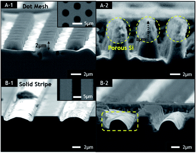
Fig. 1 shows tilted-SEM images of Si cross sections after metal-assisted chemical etching with 40 nm-thick Au catalysts for 4 and 12 minutes. Au catalyst arrays were configured with a dot mesh (4 μm diameters and 3 μm spaces) as shown in Fig. 1(A-1 and A-2) and solid stripes (8 μm widths and 6 μm spaces) as shown in Fig. 1(B-1 and B-2). Insets show top-view schematics of Au catalysts deposited on Si in the dot mesh and solid stripes before etching. After metal-assisted chemical etching, Si substrates were removed in-position of catalyst where Si was covered by Au and the bare Si portion remained unetched. Si etch rates were not uniform underneath the Au catalysts. A high etch rate at the edges and low etch rate towards the center of the metal catalysts results in metal bending, which has been reported to occur when chemical etching is performed using a micron-scale metal catalyst because of the long diffusion length of the lateral mass transport.16 Dot mesh arrays in Fig. 1(A-1) exhibited a relatively flat topology with an etch rate of 0.6 μm min−1. On the other hand, solid stripe catalysts in Fig. 1(B-1) were substantially bent with negligible removal of Si at the center of the catalyst. In addition to catalyst bending, 2 μm of lateral etching occurred in the bare Si that had not been deposited with the Au catalyst.25,26 After an extended duration of etching (12 minutes), a Si pillar array formed on the dot mesh, as shown in Fig. 1(B-1), with a slightly enhanced etch rate of 0.7 μm min−1. The topology of Si pillars seemed to be porous, especially the top portion. There was very little progress in the chemical etching of solid stripe arrays and the topology of Si appeared to be severely deformed, as shown in Fig. 1(B-2).
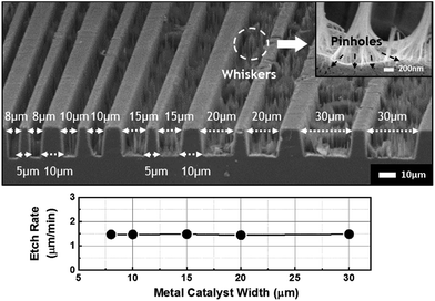
Tilted SEM images of cross-sectional Si after metal-assisted chemical etching with 20 nm-thick Au catalysts for 10 minutes are shown in Fig. 2. Au catalysts of solid stripes having a variety of widths of 8, 10, 15, 20, and 30 μm for spaces of 5 and 10 μm were etched simultaneously. Although inset in Fig. 2 shows many nano-pinholes and whiskers at the bottom of localized trench of metal catalyst after chemical etching, overall surface topologies and etch uniformity of 20 nm-thick Au catalysts were remarkably improved than those of 40 nm-thick Au catalysts. Chemical etching of Si occurred in-position of the Au catalyst, resulting in the formation of high aspect ratio trench arrays. Surface topology of 20 nm-thick Au catalysts remained fairly flat. As compared to 40 nm thick Au stripe arrays (width of 8 μm), deformation of 20 nm thick Au stripes did not occur in the micron-scale stripe arrays (width of 8 μm–30 μm). In addition, an enhanced etch rate of 1.51 μm min−1 was obtained, and this etch rate remained almost identical for all widths of Au catalysts as shown in the plot. The dramatic changes in etching uniformity and rates according to Au catalyst thickness suggest that mass transport has to be interpreted as a function of metal catalyst thickness. Long diffusion length of lateral mass transport associated with a micro-scale metal catalyst is not a dominant mechanism in metal-assisted chemical etching with 20 nm-thick Au catalysts. Another interesting feature to note is the formation of nano-scale Si whiskers, as shown in the high resolution SEM image (inset). A number of nano-pinholes tended to form as a result of the dynamic redistribution of Au from a cyclic reaction involving cycling of Au3+ back to Au0.27–29 As metal-assisted chemical etching occurred underneath the micron-scale metal catalyst, nano-scale local etching occurred simultaneously through the pinholes. Pinholes played a decisive role in determining the mass transport mechanism; this will be detailed subsequently.
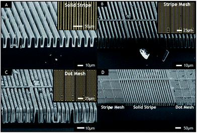
Tilted-SEM images of cross-sectional Si after metal-assisted chemical etching with 20 nm-thick Au catalysts for 15 minutes are compared in Fig. 3. Three different types of micro-scale Au catalysts were deposited on Si for metal-assisted chemical etching: (A) solid stripe (8 μm stripe widths and 8 μm spaces) arrays, (B) stripe mesh arrays (2 μm stripe widths and 5 μm spaces), (C) dot mesh arrays (4 μm dot diameters and 3 μm spaces), and (D) all features. Insets show top-view schematics of Au catalysts deposited on Si in dot mesh and solid stripe arrays before etching. Note that consistent chemical etching occurred for all stripes and dots in meshes and solid features. Almost identical etching rates were measured for the differently shaped catalyst features. Overall etching rate increased to 2.0 μm min−1 as the duration of chemical etching was extended. Surface topology and etching uniformity were dramatically improved when 20 nm-thick Au catalysts were used for metal-assisted chemical etching of Si rather than 40 nm-thick Au catalysts. The Si remaining between the trenches did not appear to be porous. Metal catalyst bending and non-uniform etching rates associated with micron-scale metal catalysts did not appear. To apply metal-assisted chemical etching to fabricate various 3D semiconductors with a high aspect ratio structure, uniform etching regardless of metal catalyst pattern shape and size is important. High aspect ratio trench, fin, and wire arrays were readily fabricated on Si substrates from stripe mesh, dot mesh, and solid strip arrays, respectively. Long diffusion length of lateral mass transport does not necessarily limit the mass transport of reactants and byproducts during chemical etching. Our results suggest that metal-assisted chemical etching of Si with controlled metal catalyst processing has potential for application in a wide range of fields.
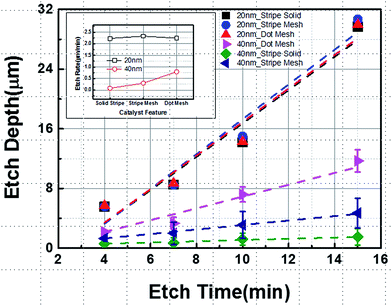
Fig. 4 compares etch depth and rates (inset) as a function of etching time for a various metal catalyst features. When 40 nm thick Au catalysts were used for micron-scale chemical etching, the etch depth was not uniform and showed strong dependency on catalyst features. Dot meshes exhibited relatively higher etch rates than solid stripe arrays. As confirmed in the physical analysis, porous Si and catalyst bending were observed for 40 nm thick Au catalysts. Wide error bars with a low etch rates indicate unsuccessful metal assisted chemical etching of Si. On the other hand, when the Au catalysts were thinned to 20 nm, uniform etch rates were measured for all features of metal catalysts (stripe solid, stripe mesh, and dot mesh arrays). Etch rates of 20 nm catalysts increased substantially without porous Si and catalyst bending phenomena. Despites many advantages afforded by metal-assisted chemical etching, non-uniform etch rates and deformation of micron-scale catalysts potentially limited the application of this technique. Our results suggest that tailoring metal catalysts enables micro-scale chemical etching for various features of metal catalysts. Subsequent discussion will detail mass transport of metal catalyst during the chemical etching.
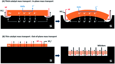
Fig. 5 illustrates mass transport mechanisms of (A) in-plane mass transport and (B) out-of-plane mass transport for metal-assisted chemical etching of Si substrates. Catalytic reactions of Au reduce the activation energy of the chemical reduction of H2O2, and injected electronic holes (h+) oxidize the Si substrates selectively beneath the catalyst. Mass transport of reactant (HF) and byproduct (SiF62−) is required for chemical etching of Si with catalytic reactions. When the metal catalyst is thick without pinholes as in Fig. 5(A), mass transport occurs only at the edge of the metal/semiconductor interface (in-plane mass transport) where etchant can directly touch the porous Si. A signature characteristic of in-plane mass transport during chemical etching is metal catalyst bending because of a relatively fast etch rate at the edge of the metal/semiconductor and a low etch rate towards the center. Excess holes not consumed by chemical etching diffused out towards the bare Si and lateral etching was also observed. When a thick metal catalyst was used, dot mesh and stripe arrays exhibited substantially different surface topology. Thermally activated redox processes with catalytic reactions are believed to be identical for both dot mesh and stripe arrays. Localized chemical reactions for removing oxidized Si are then responsible for the overall etch rates. Results suggest that in-plane mass transport was dominant and essentially no out-of-plane mass transport occurred through the 40 nm Au catalyst. Under this condition, geometrically, dot mesh arrays provided diffusion pathways for mass transport around the perimeters of the dots, which resulted in a relatively flat surface topology. On the other hand, stripe arrays had a longer diffusion distance compared to dot mesh arrays. When the metal catalyst is thin, several pinholes formed on the metal catalyst as in Fig. 5(B). Mass transports of reactant and byproducts for chemical etching may occur through the pinholes (out-of-plane mass transport). Since the etchant reaches the porous Si through the pinholes, chemical etching occurs concurrently in every location underneath the metal catalyst. Out-of-plane mass transport dramatically improved the etching uniformity at the edge and center of the metal/semiconductor interface. High aspect ratio 3-D structures were readily fabricated with high anisotropic etching characteristics. Injected holes were instantly consumed in the chemical reaction and lateral etching towards the bare Si was negligible.
Overall etch rates increased as out-of-plane and in-plane mass transports occurred simultaneously. Out-of-plane etching becomes dominant with more pinholes, which is determined by the metal catalyst thickness. With sufficient catalytic reactions beneath the thin metal for injecting electronic holes into the Si, oxidized Si beneath the metal catalyst is easily removed without metal catalyst bending. When a thin metal catalyst was used, stripe mesh, dot mesh, and stripe arrays exhibited uniform etching rates and improved surface topology. Results suggest that the geometric distance for in-plane mass transport of the chemical reaction is not a sole diffusion pathway for reactants and byproducts during etching. As the metal catalyst becomes thinner, out-of-plane mass transport is involved in the chemical reaction, which facilitates ion flux through the metal catalyst. When out-of-plane mass transport becomes dominant, the chemical reaction to remove Si occurs concurrently underneath the metal catalyst, which results in a uniform etch rate without metal bending for all catalyst features. To date, most research on metal-assisted chemical etching has been conducted with nano-scale 3-D architecture. Substantial deformation of the metal catalyst tended to occur when this technique was applied to micron-scale architecture. In-plane and out-of-plane mass transport mechanisms were consistent with experimental results, suggesting the possible fabrication of micron-scale 3-D architecture by metal-assisted chemical etching. In-plane mass transport conventionally accounted for non-uniform chemical etching and deformation of the metal catalyst since mass transport occurs only at the edge of the metal/semiconductor interface. Results confirmed that out-of-plane mass transport is dominant in chemical etching through nano-pinholes as the metal catalyst becomes thinner. Dramatic changes in etching rate and surface topology could be attributed to combined reactions of in-plane and out-of-plane mass transport.
Conclusions
We have demonstrated micron-scale metal-assisted chemical etching of Si substrates. Experimental results were interpreted in the context of metal catalyst thickness and pinhole formation. When a 40 nm thick Au catalyst was used, chemical reactions were governed by in-plane mass transport that occurred only at the interface between the Si wafer and the metal catalyst. After thinning the Au catalyst to 20 nm, out-of-plane mass transport occurred through the pinholes in the metal catalyst. Pinholes generated in the thin catalyst determined the dominant mass transport mechanism. Results suggest that a wide range of 3-D semiconductors can be fabricated by tailoring the metal catalyst to control the mass transport mechanism.Acknowledgements
This research was supported by the MSIP (Ministry of Science, ICT and Future Planning), Korea, under the “IT Consilience Creative Program” (IITP-2015-R0346-15-1008) supervised by the IITP (Institute for Information & Communications Technology Promotion). This research was also supported by a grant from the Basic Science Research Program through the National Research Foundation of Korea (NRF) funded by the Ministry of Education, Science and Technology (2013R1A1A2012111), by the Future Semiconductor Device Technology Development Program (10044735, 10048536) funded by MOTIE (Ministry of Trade, Industry & Energy) and KSRC (Korea Semiconductor Research Consortium), and by the IT R&D program of MOTIE/KEIT (10048931, the development of epi-growth analysis for next generation semiconductor and power semiconductor fundamental technology).Notes and references
- J.-P. Colinge, Solid-State Electron., 2004, 48, 897–905 CrossRef CAS PubMed.
- L.-F. Cui, R. Ruffo, C. K. Chan, H. Peng and Y. Cui, Nano Lett., 2008, 9, 491–495 CrossRef PubMed.
- Y. Cui, Z. Zhong, D. Wang, W. U. Wang and C. M. Lieber, Nano Lett., 2003, 3, 149–152 CrossRef CAS.
- J. Goldberger, A. I. Hochbaum, R. Fan and P. Yang, Nano Lett., 2006, 6, 973–977 CrossRef CAS.
- X. Cao and S. Arthur, Appl. Phys. Lett., 2004, 85, 3971–3973 CrossRef CAS PubMed.
- Z. Fan, H. Razavi, J.-W. Do, A. Moriwaki, O. Ergen, Y.-L. Chueh, P. W. Leu, J. C. Ho, T. Takahashi and L. A. Reichertz, Nat. Mater., 2009, 8, 648–653 CrossRef CAS PubMed.
- K. Yu and J. Chen, Nanoscale Res. Lett., 2009, 4, 1–10 CrossRef CAS.
- X. Li and P. Bohn, Appl. Phys. Lett., 2000, 77, 2572–2574 CrossRef CAS PubMed.
- Z. Huang, N. Geyer, P. Werner, J. de Boor and U. Gösele, Adv. Mater., 2011, 23, 285–308 CrossRef CAS PubMed.
- X. Li, Curr. Opin. Solid State Mater. Sci., 2012, 16, 71–81 CrossRef CAS PubMed.
- M. DeJarld, J. C. Shin, W. Chern, D. Chanda, K. Balasundaram, J. A. Rogers and X. Li, Nano Lett., 2011, 11, 5259–5263 CrossRef CAS PubMed.
- K. Peng, Y. Xu, Y. Wu, Y. Yan, S. T. Lee and J. Zhu, Small, 2005, 1, 1062–1067 CrossRef CAS PubMed.
- Z. Huang, H. Fang and J. Zhu, Adv. Mater., 2007, 19, 744–748 CrossRef CAS PubMed.
- S. H. Kim, P. Katal Mohseni, Y. Song, T. Ishihara and X. Li, Nano Lett., 2015, 15, 641–648 CrossRef CAS PubMed.
- K. Rykaczewski, O. J. Hildreth, C. P. Wong, A. G. Fedorov and J. H. J. Scott, Nano Lett., 2011, 11, 2369–2374 CrossRef CAS PubMed.
- N. Geyer, B. Fuhrmann, Z. Huang, J. de Boor, H. S. Leipner and P. Werner, J. Phys. Chem. C, 2012, 116, 13446–13451 CAS.
- K. Balasundaram, J. S. Sadhu, J. C. Shin, B. Azeredo, D. Chanda, M. Malik, K. Hsu, J. A. Rogers, P. Ferreira and S. Sinha, Nanotechnology, 2012, 23, 305304 CrossRef PubMed.
- A. I. Hochbaum, D. Gargas, Y. J. Hwang and P. Yang, Nano Lett., 2009, 9, 3550–3554 CrossRef CAS PubMed.
- S. Cruz, A. Hönig-d'Orville and J. Müller, J. Electrochem. Soc., 2005, 152, C418–C424 CrossRef CAS PubMed.
- I. S. Chun, E. K. Chow and X. Li, Appl. Phys. Lett., 2008, 92, 191113 CrossRef PubMed.
- J. Huang, N. Goel, H. Zhao, C. Y. Kang, K. S. Min, G. Bersuker, S. Oktyabrsky, C. K. Gaspe, M. B. Santos, P. Majhi, P. D. Kirsch, H. H. Tseng, J. C. Lee and R. Jammy, InGaAs MOSFET performance and reliability improvement by simultaneous reduction of oxide and interface charge in ALD (La)AlOx/ZrO2 gate stack, in IEDM Tech. Dig., 2009 Search PubMed.
- W. Xia, J. Zhu, H. Wang and X. Zeng, CrystEngComm, 2014, 16, 4289–4297 RSC.
- C. Chartier, S. Bastide and C. Lévy-Clément, Electrochim. Acta, 2008, 53, 5509–5516 CrossRef CAS PubMed.
- X. Geng, Z. Qi, M. Li, B. K. Duan, L. Zhao and P. W. Bohn, Sol. Energy Mater. Sol. Cells, 2012, 103, 98–107 CrossRef CAS PubMed.
- Y. Song and J. Oh, J. Mater. Chem. A, 2014, 2, 20481–20485 CAS.
- C.-L. Lee, K. Tsujino, Y. Kanda, S. Ikeda and M. Matsumura, J. Mater. Chem., 2008, 18, 1015–1020 RSC.
- Z. R. Smith, R. L. Smith and S. D. Collins, Electrochim. Acta, 2013, 92, 139–147 CrossRef CAS PubMed.
- Y. Song, B. Ki, K. Choi, I. Oh and J. Oh, J. Mater. Chem. A, 2014, 2, 11017–11021 CAS.
- X. Geng, B. K. Duan, D. A. Grismer, L. Zhao and P. W. Bohn, Electrochem. Commun., 2012, 19, 39–42 CrossRef CAS PubMed.
| This journal is © The Royal Society of Chemistry 2015 |

