Tongchuan Gaoa,
Po-Shun Huangb,
Jung-Kun Leeb and
Paul W. Leu*a
aDepartment of Industrial Engineering, University of Pittsburgh, Pittsburgh, PA 15261, USA. E-mail: pleu@pitt.edu
bDepartment of Mechanical Engineering & Materials Science, University of Pittsburgh, Pittsburgh, PA 15261, USA
First published on 10th August 2015
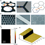
We report a comprehensive study on the optical and electronic properties of hierarchical metal nanomesh (NM)/microgrid (MG) structures to determine their performance as transparent conductors (TCs). The NM helps deliver or collect carriers locally while the lower resistance MG transports carriers over larger distances. The structures exhibit high uniformity of optical and electronic properties. Hierarchical Ag NM/Ag MG structures demonstrate 83% diffusive transmission at a sheet resistance of 0.7 Ω per square when fabricated directly on quartz and 81% at 0.7 Ω per square when fabricated directly on flexible plastic. The direct current to optical conductivity ratios σdc/σop of these structures are 2900 and 2300, respectively. This corresponds to over an order of magnitude reduction in sheet resistance with a negligible to slight reduction in transmission compared to NMs. The haze factor of these structures may be tuned by modifying the NM hole diameter. Furthermore, the hierarchical structures exhibit good durability under bending and heating.
A variety of nanostructured materials have emerged as potential substitutes for ITO and other doped metal oxides, such as percolation networks of metal nanowires (NWs)5,6 or carbon nanotubes,7 metal nanomeshes (NMs),8 nanoparticle wire arrays,9 graphene-based materials,2,10,11 and hybrid structures.12,13 Percolation network films fabricated by solution-based methods and vacuum filtration7,14 have demonstrated comparable optical transmission and sheet resistance to ITO films.5,15–17 However, it is desirable to further reduce Rs to minimize the Joule loss in current-driven devices.18
For percolation network films, Rs is inherently limited by contact resistance19 and percolation effects.20 A variety of post-treatment methods, such as thermal annealing,15 plasmonic welding,21 and chemical linking22 have been studied to reduce the wire–wire contact resistance without much loss in transparency. Metal NW films with larger NW diameters and pitches tend to have better TC performance.23,24 However, a large separation between NWs will result in poor localized conductivity and thus, poor uniform carrier collection or delivery. This is especially a problem for organic optoelectronic devices, which have short exciton diffusion lengths.25 Moreover, the percolation effects will be more pronounced due to the sparseness and the randomness of the networks. Conductive polymers have been used to relieve the percolation effect and achieve a smooth surface.26,27
Recently, hierarchical structures have been demonstrated for TCs with very low sheet resistance and excellent transparency.8,18 For example, random Ag NW films have recently been combined with mesoscale wires (widths from 1 to 5 μm) to demonstrate T = 92% at Rs = 0.36 Ω per sq or a σdc/σop of over 12000.18 The ratio of dc conductivity to optical conductivity σdc/σop is a commonly used figure of merit (FoM) for TCs.28 However, these structures suffer from some of the same contact resistance issues of random NW films and for example, must be annealed at 200 °C for 40 minutes to fuse the different length scale wires. The randomness of the structure may also result in less uniform sheet resistance and optical properties over micron length scales. We have also recently demonstrated a hierarchical structure that integrates high quality graphene grown by CVD with a metal grid to achieve T = 94% at Rs = 0.6 Ω per sq or a σdc/σop of almost 9000.12
In this paper, we conducted both simulations and experiments to investigate the performance of hierarchical Ag nanomesh (NM)/Ag microgrid (MG) structures as TCs. The hierarchical structure exhibits diffusive transmission T = 83% at Rs = 0.7 Ω per sq or σdc/σop = 2900 when fabricated on a quartz substrate and T = 81% at Rs = 0.7 Ω per sq or σdc/σop = 2300 when fabricated on a polyethylene terephthalate (PET) substrate. In contrast, Ag NMs fabricated on quartz exhibit T = 83% at Rs = 13 Ω per sq or σdc/σop = 140. The sheet resistance of the NM may be decreased by over an order of magnitude with only a slight decrease in transmission by integration with the MG. The hierarchical structures also exhibit more uniform resistance and optical properties on the microscale compared with random networks of nanowires. We demonstrate the tunability of haze factor in our NM/MG structures, which is important for various optoelectronic applications. In addition, we performed durability experiments to assess the performance of the Ag NM/MG under various bending and heating conditions.
Fig. 2(a) plots the relationship between diffusive transmission and sheet resistance for the hierarchical NM/MG structures along with various other TCs in the literature. The data for Ag NM/MG structures are plotted with various shades of blue for simulations and experiments on quartz and PET substrates. Experimentally fabricated Ag NM data on quartz and PET substrates are plotted with different shades of green. Our transmission data are plotted at the wavelength λ = 550 nm, which is near the middle of the visible spectrum. The effect of the substrates has been excluded. For comparison purposes, we plot simulation data for ITO thin films15 as well as our previously reported Cu NMs on quartz and PET substrates.8
![]() | ||
Fig. 2 (a) Transmission versus sheet resistance for TCs. Our Ag NM/MG data is shown in shades of blue and NM data is shown in shades of green at λ = 550 nm. Data for Cu NMs on quartz and PET substrates8 and simulated ITO thin films15 is also shown. (b) FoM versus sheet resistance for the same data. |
Ag NMs exhibit comparable performance to ITO thin films and Cu NMs. The Ag NMs exhibit similar performance to Cu NMs because the transmission properties at the length scales involved are primarily independent of the material, and the resistivity of Ag is close to that of Cu.23,24 The Ag NMs fabricated on rigid quartz performs slightly better than that fabricated on PET due to the better uniformity and ordering of the structure.8 The Rs of the Ag NMs is between 13 and 21 Ω per sq with about 83% transmission on quartz, and on PET, Rs is between 16 and 20 Ω per sq with a transmission between 81% and 83%. By integrating the Ag NM with the MG, the sheet resistance may be decreased substantially by over an order of magnitude without significant decrease in transmission. The Rs of the hierarchical Ag NM/MG on quartz is between 0.4 and 0.7 Ω per sq with a transmission between 74% and 83% and on PET is between 0.6 and 0.7 Ω per sq with a transmission between 77% and 81%. Our data demonstrates that Ag NM/MG samples fabricated on quartz substrates or PET substrates exhibit superior performance to ITO films. The FoM σdc/σop can be represented in terms of T and Rs by , where Z0 = 377 Ω is the free space impedance. The Ag NM has a σdc/σop of between 80 and 140. However, typical industry requirements are σdc/σop = 350.2 Fig. 2(b) plots the FoM σdc/σop of these TCs versus sheet resistance. By integrating the NM with the MG, we can improve σdc/σop drastically to over 2000.
Fig. 3(a) plots both the simulated and experimentally measured (on quartz) diffusive transmission spectrum for the hierarchical structure with aNM = 2000 nm, wNM = 100 nm, tNM = 30 nm, aMG = 200 μm, wMG = 5 μm, and tMG = 1 μm. The simulated and experimental transmission spectra are reasonably close to each other, where the minor differences can be accounted for by statistical variations and imperfections in the fabricated structure. The simulated Rs for this geometry is 0.67 Ω per sq while the measured Rs was 0.70 Ω per sq. The haze factor, defined as , is an important property for transparent conductors, where T is the diffusive transmission and Tspec is the specular transmission.31 The haze factor of the hierarchical metal NM/MG transparent conductors is tunable by changing the geometric parameters and materials. The haze factor is mostly determined by diffraction and scattering from the NM, because its dimensions are of the same magnitude as the wavelength of incident light. The MG only introduces a geometric shadow because its features are larger than the wavelengths involved. We investigated the haze factor for Ag NM/MGs with geometric parameters aMG = 500 μm, wMG = 5 μm, tMG = 1 μm, aNM = 2000 nm, tNM = 20 nm, and various wNM using both simulation and experiments. Fig. 3(c) shows (i) the simulated and (ii) the experimentally measured diffusive and specular transmission versus sheet resistance for Ag NM/MGs on quartz. In the simulation, wNM ranges from 50 nm to 200 nm to match the experimental geometry. The haze factor of experimentally fabricated Ag NM/MGs demonstrate the same overall trends as the simulated data, but the haze factor is higher than the simulation results due to imperfections in the surfaces and NM periodicity. The simulated haze factor increases from 8% to 15% as wNM increases from 50 nm to 200 nm, while Rs decreases from 1.6 to 1.4 Ω per sq. The haze factor in the fabricated samples increases from 17% to 26%, while Rs decreases from 2.0 to 1.4 Ω per sq correspondingly. The haze factor of the NM/MG can be tuned while maintaining a low sheet resistance because the overall conductance of the NM/MG is primarily due to the MG. As the NM width increases, the hole diameter decreases and the Airy pattern from Fraunhofer diffraction broadens.32 This results in a higher fraction of photons transmitted at nonnormal angles. The tunability of haze factor is important for solar cells because a high haze factor is desirable for increasing the coupling of light into the absorber.
Lastly, various durability tests were performed to evaluate the robustness of the Ag NM/MG in applications. Fig. 4(a) shows the variation in the resistance of two Ag NM/MG samples on PET substrates after both bending in compression and tension. Two Au contacts were deposited on the samples using an e-beam evaporator, and the resistance between the two contacts was monitored after bending. The samples were bent around a steel rod with 1 cm diameter with the structure toward and away from the rod for compression and tension tests, respectively. The samples for both bending tests have a geometry of aNM = 2000 nm, and wNM = 100 nm, tNM = 30 nm, aMG = 500 μm, wMG = 10 μm, and tMG = 1 μm. The original resistance of the samples prepared for the tension and compression tests are 4.3 Ω per sq and 4.0 Ω per sq, respectively. After 200 cycles of bending, the resistance of the samples are 6.1 Ω per sq and 5.3 Ω per sq, corresponding to a 39.5% and 32.5% increase, respectively. The degradation of the sample is mainly due to the delamination of the Ag MG from the SiO2 coated PET substrate, as shown in Fig. 4(b)(i). The Ag NM, which is more resilient under bending,8 is mostly intact after the bending test, as shown in Fig. 4(b)(ii). In locations where the MG has delaminated, the underlying NM is also removed, suggesting a strong mechanical connection between the two metal layers.
Fig. 4(c) shows the change in resistance of a Ag NM/MG on PET substrate after the heating test. The sample morphology is aNM = 2000 nm, wNM = 150 nm, tNM = 30 nm, aMG = 500 μm, wMG = 10 μm, and tMG = 1 μm. After continuous heating for 168 hours (h) on a hot plate at 65 °C, the resistance of the sample changed from 2.0 to 2.7 Ω per sq, increasing by 35%. Ag is prone to oxidation and passivation of the sample may help reduce sheet resistance degradation, especially at higher temperatures.33
Footnote |
† Electronic supplementary information (ESI) available: Details of simulation methods; design criterion of the hierarchical Ag NM/MG; and fabrication process of Ag MG. See DOI: 10.1039/c5ra14851k |
This journal is © The Royal Society of Chemistry 2015 |