DOI:
10.1039/C5RA12617G
(Paper)
RSC Adv., 2015,
5, 70707-70712
Inkjet-printed transparent nanowire thin film features for UV photodetectors
Received
30th June 2015
, Accepted 13th August 2015
First published on 13th August 2015
Abstract
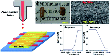
In this study, a simple and effective direct printing method was developed to print patterned nanowire thin films for UV detection. Inks containing silver or titanium dioxide (TiO2) nanowires were first formulated adequately to form stable suspension for inkjet printing applications. Sedimentation tests were also carried out to characterize the terminal velocity and dispersion stability of nanowires to avoid potential nozzle clogging problems. The well-dispersed silver nanowire ink was then inkjet printed on PET films to form patterned electrodes. Above the electrodes, another layer of TiO2 nanowires was also printed to create a highly transparent photodetector with >80% visible transmittance. The printed photodetector showed a fairly low dark current of 10−12–10−14 A with a high on/off ratio of 2000 to UV radiation. Under a bias voltage of 2 V, the detector showed fast responses to UV illumination with a rise time of 0.4 s and a recovery time of 0.1 s. More photo currents can also be collected with a larger printed electrode area. In summary, this study shows the feasibility of applying inkjet printing technology to create nanowire thin films with specific patterns, and can be further employed for photoelectric applications.
Introduction
Transparent devices are some of the most promising technologies for next generation electronic systems,1 and have recently attracted great interest due to their potential impact in fields like transparent displays, transparent energy storage, and solar cells.2–5 To achieve high transparency as well as great functionality, one-dimensional (1D) nanostructure materials, such as nanowires or nano-ribbons, have been widely adopted in the fabrication processes of various transparent electronic devices. For example, the percolating networks in silver nanowire (AgNW) thin film coatings can provide a highly conductive medium with great transparency, and have been considered as a promising transparent conductive material for flexible or stretchable optoelectronic devices.6–9 However, the deposition methods of nanowire materials, such as spin or spray coating, need pre-defined masks to create thin film patterns, and thus yield vast amounts of material waste. In contrast, inkjet printing, a direct writing method with nearly no material waste, has been widely employed to fabricate electric devices with great precision and flexibility. However, nozzle clogging problems are frequently encountered in inkjet-printing particulate inks, and hence stringent conditions, such as low precipitation and small particle sizes, are required in the ink formulation step. Because of the high aspect ratios, the longer dimension of 1D nanomaterials is regularly in the range of micrometers and leads to relatively fast precipitation.
Thus, 1D materials are rarely printed by inkjet devices due to printing and dispersion problems.10 The printability of 1D nanomaterial dispersion from inkjet nozzles remains a challenging issue and should be addressed for future applications in transparent printed electronics. Recent research has shown that AgNWs can be used to print conductive thin film features. Wu et al. inkjet printed AgNW/silver nitrate mixture,11 and showed that the addition of AgNWs enhances the conductivity of the printed composite structures after annealing at 200 °C. Recently, Finn et al.12 inkjet printed pristine AgNW on flexible transparent substrates. To avoid nozzle clogging and sedimentation problems, the length of AgNWs are reduced to 2.2 μm and suspended with diethylene glycol. Thus, a temperature of 110 °C in vacuum is needed to evaporate the solvents. To improve printability and to reduce post-treatment temperature, in this study, a solvent replacement approach is used to increase the dispersion stability of AgNWs. Furthermore, AgNWs of length up to 50 μm can be printed with careful printing parameter adjustments.
One of optoelectronic devices that can benefit from high transparency is photodetector, which is a type of electronic device for light sensing and have broad optoelectronic applications, such as missile launch detection, chemical/biological analysis, and optical communications.13 Typical photodetectors make use of a layer of light sensitive material to generate photocurrents, which can be collected by a set of metal electrodes underneath the photo sensing materials. Generally, non-transparent metal electrodes such as gold (Au) and platinum (Pt) are used in these UV photodetectors,14–17 whereas metal oxides, such as TiO2, ZnO, and SnO2,18–22 are commonly adopted as the photo sensitive materials. Recent research shows that these oxide nanowires or nanobelts arrays grown vertically on metal electrodes can absorb light much more effectively than bulk oxides due to increased transparency and larger surface areas under light illumination.23–27 The fabrication methods for those upright nanostructures, however, usually involve multiple processing steps with high temperature chemical reactions, and cannot be easily employed to create thin film patterns. Alternatively, Sheng Xu et al. showed that lateral nanowire networks can still have great light absorbing performance,28 and therefore solution-based or printed oxide nanowire thin films can still be functional after deposition. Moreover, Afal et al. demonstrated that transparent AgNW electrodes can also enhance the light absorbing performance.29 Thus, if it is possible to print both metal and oxide nanowire thin films with a feasible inkjet printing method, one can directly fabricate photodetectors with specific patterns with good light absorption performance.
In this article, a simple direct printing method is developed to print transparent nanowire thin films and will be used in fabricating photodetectors. First, formulation process for inks containing nanowires will be studied to provide stable suspensions. Inkjet printing process with consistent drop ejection will also be carefully investigated to explore the feasibility of creating fine feature patterns of nanowire thin films. A layer-by-layer strategy will then be used to fabricate photodetectors with patterned electrodes. The characteristics of the printed photodetectors, such as on/off ratio and rise/recovery times, will be carefully examined to show the performance of the printed devices.
Experimental
Materials
Anhydrous ethanol, acetone, and isopropanol (IPA) were supplied by Sigma-Aldrich, USA, and were used as received. Deionized water (Millipore Milli-Q grade) with a resistivity of 18.2 MΩ cm−1 was used in the experiments. Silver nanowire (AgNW, 120 nm in diameter and 20–50 μm in length, 0.5 wt% in IPA) solution and titanium dioxide (TiO2) nanowire (100 nm in diameter and 10 μm in length) powder were purchased form Sigma-Aldrich, USA. Flexible PET slides (Universal films, Japan) of 2.5 × 2.5 cm were cleaned by rinsing sequentially with deionized water, ethanol, and IPA in ultrasonic bath (DELTA DC300H), and were dried in a vacuum oven at 60 °C.
Ink preparation
The AgNW/IPA suspension was prepared by directly diluting the purchased AgNW solution with IPA to form a 0.8 mg mL−1 solution. The aqueous silver nanowire ink was prepared by replacing IPA with deionized water to form a 0.8 mg mL−1 AgNW aqueous solution as follows: (i) the purchased AgNW suspension was centrifuged at 1500 rpm for 15 minutes to collect the sediments. (ii) The sediment was rinsed by acetone and dried in air at room temperature to remove the residual solvents. (iii) The dried AgNW was mixed with proper amount of deionized water and was put in an ultrasonic bath for 30 minutes to obtain a 0.8 mg mL−1 aqueous AgNW suspension. Titanium dioxide (TiO2) nanowire solution was prepared by mixing TiO2 powder with deionized water to form a 5 mg mL−1 TiO2 nanowire suspension. The suspension was sonicated in a sonication bath for 30 minutes to ensure the suspension stability. The viscosities were 0.98 cp and 1.02 cp, which were measured by a Brookfield DV-III Ultra Rheometer at 20 °C, for AgNW and TiO2 nanowire inks, respectively.
Printing procedures and measurements
Ink stability was measured by LUMisizer (LUM GmbH, Germany). The drop deposition was made by a MicroFab JetLab4 system (MicroFab Technologies Inc., USA). Both silver and TiO2 nanowire inks were ejected from a 50 μm nozzle to form droplets of 40 μm at a speed of 5 m s−1 and a frequency of 850 Hz. The as-printed samples were heated on a hotplate at 100 °C for 30 minutes to remove remaining solvents or moisture. The microstructures of printed samples were examined with scanning electron microscopy (Nova NanoSEM 230, FEI Company, USA). The electrical characteristics were carried out using a Keithley 4200 semiconductor parameter analyser (Keithley Instruments Inc., USA).
Results and discussion
Stability of the nanowire inks
Consistent droplet sizes and ejection speed is crucial to printing quality for inkjet applications. To achieve stable and consistent droplet ejection, one needs to avoid clogging around inkjet printhead or in the ink supply system. Because the purchased AgNWs are dispersed in IPA, a highly volatile solvent, clogs near the printing nozzle happen and droplets cannot be consistently ejected. To avoid this clogging problem, the AgNWs are dried and re-dispersed in water. As shown in Fig. 1(a), the simple sedimentation test shows that the re-dispersed AgNWs have a much slower sedimentation rate, possibly because of the ionized AgNW surfaces in water. The aqueous AgNW dispersion shows no obvious sediments for nearly one day, while AgNW/IPA precipitates totally in the same time period. To further quantify the sedimentation speed, the positions of the supernatant/sediment interface are determined from the transmittance spectra of LUMisizer. Under a centrifugal force of 520 × g, the sedimentation speed of the aqueous is 85.6 μm s−1, much slower than the speed of 180.4 μm s−1 for the original AgNW/IPA dispersion. This measurement means that under regular gravity condition, the sedimentation rate can be as low as 1.4 cm per day, which is roughly the same as observed in Fig. 1(b) and fulfils the minimum requirement for regular inkjet printing devices. However, for industrial printhead, a slower sedimentation rate is required and more research is necessary to prevent clogging in ink supply channels.
 |
| Fig. 1 Stability tests for AgNW inks: (a) sedimentation process of AgNW dispersed in DI water and IPA under regular gravity. Both samples have the same AgNW volume fraction and were put in sonication bath for an hour before the test. (b) Interface positions determined by Lumisizer analysis for AgNW dispersed in water and IPA under a centrifugal force of 520 × g. | |
Printing and patterning with nanowire inks
AgNW electrodes. With the proper ink formulation, droplets of AgNW dispersion can be ejected consistently without suspension stability or solvent volatility issues (Fig. 2(a)). Each ejected droplet forms a circular spot with a diameter of ∼45 μm (Fig. 2(c)). By tuning the dot-to-dot spacing down to 45 μm, one can easily create straight lines (Fig. 2(e)) or filled solid patterns (Fig. 3(a–c)). The printed lines or thin films are composed of continuous AgNW networks (Fig. 2(b)), and thus are fairly conductive. One can further increase the conductivity by stacking layers of AgNW. However, it is noticeable that the printed silver track in Fig. 2(b) is not perfectly straight with sharp edges, possibly due to the low fluid viscosity and slight ink feathering.
 |
| Fig. 2 (a) Sequential images of drop formation from an inkjet nozzle. (b) SEM image of a printed line composed of silver nanowires. Microscopic images of silver nanowire line printed on PET substrates with different dot-to-dot spacing distances: (c) 60 μm, (d) 50 μm, (e) 45 μm. | |
 |
| Fig. 3 Various printed patterns of silver nanowires: (a) a multi-layer straight line, (b) a rectangular thin film, (c) an NTU symbol printed. (d) Variation in sheet resistance with number of printed layers. The inset pictures are the images of printed thin films under optical microscopy. | |
As shown in Fig. 3, with only one layer, the loose connectivity between the AgNW networks leads to a high sheet resistance of 2000 Ω sq−1. After being heated, the thermal annealing process leads to a much lower resistance of ∼500 Ω sq−1. To increase film conductivity, more AgNWs are required to increase the network connections for charge transfer.
Thus, with a second AgNW layer deposited, a better percolation network of well-connected AgNWs is formed and the sheet resistance reduces to 35 Ω sq−1. The thermal annealing, however, shows insignificant effects on the conductivity, indicating that the connection between nanowires is fairly effective for electron transfer even with simple air drying. Moreover, for AgNW thin films with more than 2 layers, because of the effective mesh percolations in the AgNW networks, the sheet resistances without thermal annealing reduces slowly and remain smaller than 100 Ω sq−1. In the following sections of printed photodetectors, 5 layers of AgNW are used for the electrodes to ensure the efficiency of photocurrent collection.
TiO2 NW thin films. Similarly to the printed AgNW thin films, TiO2 thin film patterns can also be printed easily. Before printing, aqueous TiO2 ink is formulated and shows little sediment over 12 hours. Stable ink droplets can also be ejected to form patterns similar to those shown in Fig. 2. Similar to AgNW thin films, sufficient amount of TiO2 nanowires are needed to ensure sufficient paths for charge carriers to move in nanowire networks for effective photo detection. However, in contrast to AgNW thin films, the printed TiO2 thin films are not conductive, and it is difficult to directly determine the effectiveness of mesh percolation in the nanowire networks. Therefore, SEM analysis is used to check the microstructural percolation of the printed TiO2 nanowire thin films. As shown in Fig. 4, when little amount of TiO2 nanowires are deposited on the substrate, the SEM image shows widely spread nanowires with few contact points. With more deposit amounts, the nanowire network becomes more compact with a lot more contact points. These results show that at least 5 layers of drop deposition are needed to have effective nanowire coverage to form interlacing percolations for photo current collection.
 |
| Fig. 4 (a) Images of TiO2 nanowire films of different deposit density under optical microscopy. (b) SEM images of the TiO2 nanowire structure. | |
Stacking of NW thin films
Besides the effective percolation of Ag or TiO2 nanowires thin films for effective current collections, the stacking sequence of two materials also affects the collection efficiency for photo currents. As shown in Fig. 5(a), if one prints linear AgNW patterns after TiO2 deposition, the liquid can be seeped randomly into the underlying nanostructures. Hence, the line boundaries are mostly lost and the printed AgNW thin films cannot form effective patterns for conductive electrodes.
 |
| Fig. 5 (a) Optical images of printed photodetectors with different printing sequences. The left-hand-side is TiO2 NWs deposited on Ag NW electrodes, and the other one has AgNW electrodes on the top. (b) UV-vis analysis of the transmittance spectrum shows high transparency (65–85%) of the printed photodetector under 400–700 nm wavelength. | |
On the other hand, if the AgNW lines are printed first following by TiO2, although TiO2 nanowires might still seep into AgNW network, an all-printed UV photodetector device can be obtained with functional conductive silver tracks. The printed devices show good transparency with a peak value of 85% at the upper limit of the visible range (Fig. 5(b)). The microstructures of the printed photodetectors are further examined carefully under SEM to ensure contacts between electrodes (Ag nanowires) and active layer (TiO2 nanowires). As shown in Fig. 6(a), the area around the AgNW electrode shows a dense nanowire packing with a compact network. The existence of Ag and Ti are both detected by EDX analysis (Fig. 6(b)) over the area. Different from regular electronic devices with smooth electrode requirements, here the roughness of the printed AgNW electrode enhances the contact between AgNW and TiO2 NW, and thus is favorable for photo current collection. To further determined the pattern fidelity and printing resolution, EDX mapping is used to check the spatial distribution of Ag and TiO2. As shown in Fig. 6(c), an AgNW electrode with a width of ∼50 μm and edge roughness of 5 μm, nearly the same as the original designed pattern, can be clearly recognized in the upper half of the EDX detection area, while TiO2 spread all around (Fig. 6(d)). The percolation of AgNW networks, however, seems unaffected by the later deposited TiO2 ink, and thus the pre-printed AgNW electrode remains effective for current collection in the photo sensing applications.
 |
| Fig. 6 (a) The SEM image of a printed photodetector. The area near the AgNW electrode was selected to show the interlacing networks of stacked silver and TiO2 nanowires. (b) EDX analysis shows two key elements (Ag and Ti) within the printed photodetector, (c) and (d) are the EDX elemental mapping for Ag and Ti distributions, respectively, in Fig. 6(a). One can clearly tell that silver only shows up in the top half, whereas Ti is spread over the whole area. | |
Printed UV photodetectors
The flexibility of inkjet printing technology allows the quick patterning and easy fabrication for photodetectors with high responsivity. Although the active TiO2 layer can only compose of lateral nanowire arrays due to the printing limitations, the printed photodetectors still exhibit a high on/off ratio (Fig. 7(a)), indicating the great contacts between NW–NW junctions in the printed thin film layers. In the dark state, because TiO2 is an insulating material with low charge carrier concentrations, a low dark current in the order of pA is observed. When the nanowires are subjected to UV illumination with energies larger than the bandgap of TiO2 (3–3.2 eV),30–32 electron and hole pairs are generated by absorbing UV photons, and a rapid increasing photocurrent around three orders larger (∼2000 at 2 V) is observed. This large on/off ratio is close to the observed values (ranging from 20 to 2600) in recent works18,29 with similar device architectures but with different UV detection materials (ZnO and Si nanowires).
 |
| Fig. 7 (a) The I–V characteristics of the printed photodetectors in logarithmic coordinates under UV light illumination (above) and dark condition (below). Two devices with one or three pairs of electrodes were used as indicated in the figure. (b) Highlights of the dynamic response behavior (response/recovery times) for the photodetector with three pairs of electrodes under UV illumination at 2 V bias. (c) Light on–off measurements for one-pair-electrode device and (d) three-pair-electrode device under 2 V bias. The AgNW electrodes for both devices are 50 μm wide with a pitch width of 70 μm, as shown in Fig. 5(a). | |
With an applied bias voltage of 2 V, the photodetector shows a fast response to photo illumination (Fig. 7(b)). Before UV illumination, a low dark current of 2 pA is detected. Soon after illuminated with UV light, the collected current rises quickly to 1.67 nA. The rise time can be determined as 0.4 s by calculating the time necessary for the current to increase from 10% to 90% of its saturation value. This quick response time shows that the effective percolation contacts between the Ag and TiO2 NW networks. After turning off the UV illumination, the photogenerated holes and electrons quickly recombine with each other. As a result, the charge carrier concentration in the nanowire network decreases, and leads to a fast decrease in the current response with a fall time of 0.126 s (the time necessary for the current to decrease from 90% to 10% of its saturation value).
The dynamic responses of printed photodetectors with one or three pairs are also compared to understand the effects of electrode density in photon collection. As shown in Fig. 7(c) and (d), there is no significant difference in rise or recovery times with different NW densities, indicating that NW–NW junctions determine trapping/de-trapping of the carriers. However, the collected currents can be amplified with more printed electrode pairs. With three pairs of electrodes, the photocurrent increases to 1.7 nA, almost triple as that from one pair (0.57 nA). This result indicates that the absorption of photons and generation of charge carriers can only be effectively collected near the printed electrodes, and one can easily fabricate the desired electrode systems by digitally change the design patterns with this inkjet method.
Conclusions
An inkjet printing method is developed to fabricate thin film patterns with nanowire inks. Silver and titanium dioxide nanowires are dispersed in water through a solvent replacement process to avoid potential nozzle clogging problem. Sedimentation tests show that the silver nanowire suspension has a sedimentation rate of 85.6 μm s−1 at 520 × g, and is suitable for inkjet printers. The nanowire inks are inkjet printed on a plastic substrate to form straight lines as conductive tracks for current collection. Multiple layers of silver nanowire patterns are deposited to enhance the nanowire percolation for great electrical conductivity. Similarly, TiO2 nanowire suspension with a slow sedimentation rate is printed on top of the AgNW electrodes to serve as the functional layer for photo detection. The printed photodetector is highly transparent with a visible transmittance of 85%. Because of the good electron mobility of TiO2 and its suitable UV irradiation band gap, the photodetector showed quick and great responses to UV radiation. The fabricated photodetectors has a fairly small dimension of 20 mm2, and show a low dark current of 10−12 A with a high on/off ratio of 2000. Under a bias voltage of 2 V, a fast rise time of 0.4 s can be reached with a recovery time of 0.1 seconds. A higher photo current can also be collected with more printed electrode pairs. In summary, this study shows the feasibility of applying inkjet printing technology to fabricate nanowire thin films with specific patterns, and the fabrication process can be further extended to create photoelectric devices for transparent microelectronic applications.
Acknowledgements
Ministry of Science and Technology (MOST) in Taiwan supported this research through Grants MOST 103-2923-E-002-010-MY3, 103-2923-E-002-012-MY2 and 103-2221-E-002-185-MY3.
Notes and references
- D. S. Hecht, L. Hu and G. Irvin, Adv. Mater., 2011, 23, 1482 CrossRef CAS PubMed.
- J. Y. Lee, S. T. Connor, Y. Cui and P. Peumans, Nano Lett., 2010, 10, 1276 CrossRef CAS PubMed.
- L. Li, Z. Yu, W. Hu, C. H. Chang, Q. Chen and Q. Pei, Adv. Mater., 2011, 23, 5563 CrossRef CAS PubMed.
- J. Lee, P. Lee, H. B. Lee, S. Hong, I. Lee, J. Yeo, S. S. Lee, T.-S. Kim, D. Lee and S. H. Ko, Adv. Funct. Mater., 2013, 23, 4171 CrossRef CAS PubMed.
- Z. Yu, L. Li, Q. Zhang, W. Hu and Q. Pei, Adv. Mater., 2011, 23, 4453 CrossRef CAS.
- Z. Jin, L. Gao, Q. Zhou and J. Wang, Sci. Rep., 2014, 4, 4268 Search PubMed.
- J. W. Durham 3rd and Y. Zhu, ACS Appl. Mater. Interfaces, 2013, 5, 256 Search PubMed.
- Y. Zhang, X. Wang, Y. Wu, J. Jie, X. Zhang, Y. Xing, H. Wu, B. Zou, X. Zhang and X. Zhang, J. Mater. Chem., 2012, 22, 14357 RSC.
- J. X. Wang, C. Y. Yan, W. B. Kang and P. S. Lee, Nanoscale, 2014, 6, 10734 RSC.
- H. Lu, J. Lin, N. Wu, S. Nie, Q. Luo, C.-Q. Ma and Z. Cui, Appl. Phys. Lett., 2015, 106, 093302 CrossRef.
- J.-T. Wu, S. Lien-Chung Hsu, M.-H. Tsai, Y.-F. Liu and W.-S. Hwang, J. Mater. Chem., 2012, 22, 15599 RSC.
- D. J. Finn, M. Lotya and J. N. Coleman, ACS Appl. Mater. Interfaces, 2015, 7, 9254 CAS.
- T. Zhai, L. Li, X. Wang, X. Fang, Y. Bando and D. Golberg, Adv. Funct. Mater., 2010, 20, 4233 CrossRef CAS PubMed.
- X. Gu, M. Zhang, F. Meng, X. Zhang, Y. Chen and S. Ruan, Appl. Surf. Sci., 2014, 307, 20 CrossRef CAS PubMed.
- Z. Bai, X. Yan, X. Chen, H. Liu, Y. Shen and Y. Zhang, Curr. Appl. Phys., 2013, 13, 165 CrossRef PubMed.
- X. Kong, C. Liu, W. Dong, X. Zhang, C. Tao, L. Shen, J. Zhou, Y. Fei and S. Ruan, Appl. Phys. Lett., 2009, 94, 123502 CrossRef PubMed.
- T. Y. Tsai, S. J. Chang, W. Y. Weng, S. H. Wang, C. J. Chiu, C. L. Hsu and T. J. Hsueh, IEEE Photonics Technol. Lett., 2012, 24, 1584 CrossRef CAS.
- E. Mulazimoglu, S. Coskun, M. Gunoven, B. Butun, E. Ozbay, R. Turan and H. E. Unalan, Appl. Phys. Lett., 2013, 103, 083114 CrossRef PubMed.
- G. Liu, C. Tao, M. Zhang, X. Gu, F. Meng, X. Zhang, Y. Chen and S. Ruan, J. Alloys Compd., 2014, 601, 104 CrossRef CAS PubMed.
- S. I. Inamdar and K. Y. Rajpure, J. Alloys Compd., 2014, 595, 55 CrossRef CAS PubMed.
- D. Kim, G. Shin, J. Yoon, D. Jang, S. J. Lee, G. Zi and J. S. Ha, Nanotechnology, 2013, 24, 315502 CrossRef PubMed.
- H. Xue, X. Kong, Z. Liu, C. Liu, J. Zhou, W. Chen, S. Ruan and Q. Xu, Appl. Phys. Lett., 2007, 90, 201118 CrossRef PubMed.
- C. Y. Chen, M. W. Chen, C. Y. Hsu, D. H. Lien, M. J. Chen and J. H. He, IEEE J. Sel. Top. Quantum Electron., 2012, 18, 1807 CrossRef CAS.
- B. Nie, J. G. Hu, L. B. Luo, C. Xie, L. H. Zeng, P. Lv, F. Z. Li, J. S. Jie, M. Feng, C. Y. Wu, Y. Q. Yu and S. H. Yu, Small, 2013, 9, 2872 CrossRef CAS.
- E. S. Ates, S. Kucukyildiz and H. E. Unalan, ACS Appl. Mater. Interfaces, 2012, 4, 5142 CAS.
- Y. R. Xie, L. Wei, G. D. Wei, Q. H. Li, D. Wang, Y. X. Chen, S. S. Yan, G. L. Liu, L. M. Mei and J. Jiao, Nanoscale Res. Lett., 2013, 8, 188 CrossRef PubMed.
- C. Y. Chen, J. R. D. Retamal, I. W. Wu, D. H. Lien, M. W. Chen, Y. Ding, Y. L. Chueh, C. I. Wu and J. H. He, ACS Nano, 2012, 6, 9366 CrossRef CAS PubMed.
- S. Xu, Y. Qin, C. Xu, Y. G. Wei, R. S. Yang and Z. L. Wang, Nat. Nanotechnol., 2010, 5, 366 CrossRef CAS PubMed.
- A. Afal, S. Coskun and H. Emrah Unalan, Appl. Phys. Lett., 2013, 102, 043503 CrossRef PubMed.
- Y. X. Zhang, G. H. Li, Y. X. Jin, Y. Zhang, J. Zhang and L. D. Zhang, Chem. Phys. Lett., 2002, 365, 300 CrossRef CAS.
- J. M. Wu, H. C. Shih and W. T. Wu, Nanotechnology, 2006, 17, 105 CrossRef CAS.
- X. Pan, Y. Zhao, S. Liu, C. L. Korzeniewski, S. Wang and Z. Fan, ACS Appl. Mater. Interfaces, 2012, 4, 3944 CAS.
|
This journal is © The Royal Society of Chemistry 2015 |
Click here to see how this site uses Cookies. View our privacy policy here.