DOI:
10.1039/C5RA14646A
(Paper)
RSC Adv., 2015,
5, 94679-94684
Structures and electronic properties of GaSe and GaS nanoribbons
Received
24th July 2015
, Accepted 27th October 2015
First published on 28th October 2015
Abstract
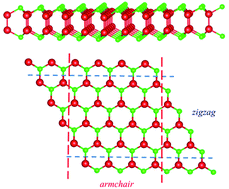
Two-dimensional (2D) semiconductor gallium monochalcogenides GaX (X = S, Se) hold great promise for future electronics and optics. In this paper, geometrical structures and electronic properties of quasi-1D pristine gallium monochalcogenide GaX (X = S, Se) nanoribbons (NRs) have been studied by means of first-principles calculations, aiming to address the edge effects of 2D GaX (X = S, Se) nanoflakes. The armchair NRs are nonmagnetic semiconductors, in which the edge distortion is observed. In the zigzag GaX NRs, they present metallic behavior for both spin-up and spin-down channels with great magnetism, except for 1-Z-NR GaSe and GaS. The spin polarization in the zigzag GaX (X = S, Se) NRs mainly originates from the unpaired electrons on the edge Ga atoms. Our present work may well complement the current studies on the layered gallium monochalcogenides GaX (X = S, Se), and other quasi-1D NRs (e.g. graphene, ZnO, and MoS2).
Introduction
The discovery of graphene, a single atomic layer of graphite, has generated enormous excitement in the last decade.1,2 It also triggers a boom for other two-dimensional (2D) layered materials. 2D layered materials such as graphene, hexagonal BN (h-BN), and transition metal chalcogenides (e.g. GaSe, MoS2, WS2) remain planar and can be separated simply by mechanical or liquid-phase exfoliation from their bulk layered solids, where exfoliation is facilitated by the weak interlayer van der Waals (vdW) forces. These 2D layered materials have a wide range of applications in field-effect transistors, spin- or valley-tronics, thermoelectrics, topological insulators, and energy conversion and storage.3–6 Nanoribbons, a quasi-1D version of the 2D materials, have also been extensively studied from both experimental and theoretical perspectives, and have been found to possess distinct properties compared with their 2D counterparts.7–9 Graphene NRs (GNRs) can be produced by cutting graphene sheets10 or by longitudinally unzipping carbon nanotubes.11 Theoretical calculations show that the hydrogen passivated GNRs with armchair or zigzag shaped edges have nonzero and direct band gaps.12 The band gaps of hydrogen passivated GNRs with armchair shaped edges originate from quantum confinement, while for those with zigzag shaped edges, the band gaps arise from a staggered sublattice potential owing to spin ordered states at the edges. Along with GNRs, studies of nanoribbons based upon other 2D materials are also drawing great interest.13–16
As a kind of layered semiconducting material, gallium monochalcogenides GaX (X = S, Se) have also attracted much research interest for their potential applications in fields such as solar energy conversion.17 Unlike graphite and layered h-BN, the monolayer of GaSe is composed of four sublayers stacked in the sequence Se–Ga–Ga–Se (GaS monolayer is similar to GaSe monolayer), as shown in Fig. 1a. Experimental efforts have since been carried out to fabricate these GaX (X = S, Se) in monolayer form, and monolayer GaX (X = S, Se) sheets have already been successfully synthesized.18–21 Soon after, theoretical calculations have also been undertaken to further understand the electronic and photonic properties of GaX (X = S, Se) monolayers.22,23 Although extensive experimental and theoretical efforts have been devoted to the investigations of the properties of 2D GaX (X = S, Se) nanosheets,18–24 to the best of our knowledge, little is known about the electronic properties of the four-atom-thick GaX (X = S, Se) nanoribbons, which are different from other nanoribbons from one-atom-thick (e.g. GNRs12 and ZnO NRs16) to three-atom-thick (e.g. MoS2 NRs13). In this work, we report a first-principles study of the geometric and electronic properties of GaX (X = S, Se) nanoribbons with armchair or zigzag shaped edges. These encouraging theoretical results would provide us a thorough and deep understanding of the novel properties of GaX (X = S, Se) nanoribbons.
 |
| Fig. 1 Optimized structure of 2D single-layer GaSe nanosheet: side view (a) and top view with its unit cell outlined (b); as well as its band structure (c) and DOS (d). | |
Methods
First-principles calculations were carried out using the Vienna ab initio simulation package (VASP).25–28 The Kohn–Sham equations were solved using the projector-augmented wave (PAW) method.29,30 The exchange and correlation interactions of valence electrons are described by the Perdew–Burke–Ernzerhof (PBE) functional31,32 within the generalized gradient approximation (GGA). For NRs, the Brillouin-zone integrations were performed on a Γ-centered Monkhorst–Pack 1 × 1 × 11 k-point grid, while for 2D single-layer GaX (X = S, Se), 16 × 16 × 1 k-point grid was applied.33 The kinetic energy cutoff for plane waves was set to 500 eV and the “accurate” precision setting was adopted to avoid wrap around errors. The convergence criterion for the electronic self-consistent loop was set to 10−5 eV. During the structural relaxations, the vacuum regions were at least 20 Å to ensure the periodic images are well separated while other lattice vectors were fully relaxed. All atoms were also relaxed until the Hellmann–Feynman forces were smaller than 0.01 eV Å−1.
Results and discussions
Before studying NRs, we first check the 2D hexagonal single-layer GaSe nanosheet, as seen in Fig. 1a and b for structures, and the 2D single-layer GaS nanosheet has a similar structure. The lattice parameter a0 is 3.820 Å and 3.637 Å for 2D single-layer GaSe and GaS nanosheet, respectively. The Ga–Ga distance is 2.474 Å and 2.476 Å in GaSe and GaS, while the Ga–Se distance is 2.500 Å and the Ga–S distance is 2.368 Å. Our calculated parameters are in excellent agreement with previous studies (e.g. a0 is 3.82 Å and 3.64 Å for single-layer GaSe and GaS nanosheet).22,23 In addition to the 2H phase in the current study, we also tested the 1T phase of single-layer GaSe nanosheet as in MoS2, but the 1T phase is 7.32 meV higher in energy per GaSe molecular formula than the 2H phase. Fig. 1c shows the band structure of single-layer GaSe. It is clear that single-layer GaSe display indirect band gap with valence band maximum (VBM) located between the Γ and M points and conduction band minimum (CBM) located at the Γ point. The calculated band gap is 1.82 eV, which agrees with the previous theoretical studies (1.91 eV).20 GaS has a similar band structure to GaSe, but with a bigger band gap 2.38 eV. We note that the PBE functional as usual underestimates the band gaps compared with hybrid functional HSE06 or quasiparticle GW method, but basic physics discovered here should not be changed. Fig. 1d shows the total and projected density of states (DOS) of single-layer GaSe. The projected DOS illustrates that the valence band of single-layer GaSe is dominated by Ga 4p and Se 4p states.
Similar to GNRs, we consider two types of GaX (X = S, Se) NRs with armchair and zigzag shaped edges, as shown in Fig. 2 for top views of GaSe (GaS is similar). Here, the NR width W is defined as the number of honeycomb units along the ribbon direction. We studied the NR with width W from one unit (1u) up to ten units (10u), as displayed in Fig. 2. More specifically, we studied the GaSe NRs with width up to 3.85 nm for armchair NR and 6.47 nm for zigzag NR. Together with following rapidly-converged electronic and magnetic properties of GaX (X = S, Se) NRs, we are confident that our results would be useful to guide the future experiments on GaX (X = S, Se) NRs with width even up to hundreds of nanometers. Take GaSe NRs as an example, and GaS NRs behave similarly. It is clear that the atoms at the edges of armchair GaSe NRs are reconstructed: while two edge Ga atoms are lowering, their adjacent edge Se atoms are raised. Similar phenomenon is also observed for other armchair NRs, such as MoS2,13 ZnS,15 and ZnO.16 For zigzag GaSe NRs, however no significant change occurs from the initial structures.
 |
| Fig. 2 Top views of armchair (a) and zigzag (b) GaSe NRs with growth direction and a width of units from one (1u) up to ten (10u). | |
The band structures for armchair GaSe NRs with different widths are shown in Fig. 3. The armchair NRs are all semiconductors with an indirect band gap. The CBM is always at the X point, while the VBM is usually at the Γ point except for W = 3u and 4u (slightly higher than the value of the Γ point, <5 meV). With the ribbon width increasing, the band gap increases from 0.62 eV (W = 1u), but converges rapidly to 1.25 eV from W = 6u, as seen in Fig. 4. This trend is quite similar to that of armchair MoS2
13 and GN14 nanoribbons, but opposite to armchair ZnO16 and ZnS15 nanoribbons. The band gaps of armchair GaSe NRs is much smaller than that of 2D GaSe sheet (1.82 eV), which is attributed to the newly introduced flat energy levels at both valence and conduction band edges by the edge atoms of nanoribbons, narrowing the band gap accordingly.13 The newly introduced flat energy level at valence band gives armchair GaSe NRs a quasi-direct band gap (from X point to X point), compared with 2D GaSe nanosheet, making armchair GaSe NRs more efficient on photovoltaics (transition from Ga-4s to Se-4p or Ga-4p as seen in Fig. 3d). The band structures for armchair GaS NRs are similar to their GaSe counterparts, but with bigger band gaps (over ca. 0.2 eV), as seen in Fig. 4. Moreover, the CBM is also at the X point, but the VBM is at the Γ point only for W = 2u and 3u. It is worth noting that the valence bond value at the Γ point is only ca. 0.02 eV lower than the according VBM, and decreases to less than 0.01 eV from W = 7u. With the ribbon width increasing, the band gap of armchair GaS NRs grows from 0.82 eV at W = 1u, and converges to 1.45 eV after W = 6u, as seen in Fig. 4.
 |
| Fig. 3 Band structures of armchair GaSe NRs of one unit (a), five units (b), ten units (c), and DOSs of armchair GaSe NRs of ten units (d). | |
 |
| Fig. 4 Band gaps of armchair GaS and GaSe NRs as a function of number of units. | |
For zigzag GaSe NRs, the band structures are shown in Fig. 5a–e. The electronic properties of zigzag GaSe NRs are quite different from those of armchair GaSe NRs. There is an indirect band (1.67 eV from Γ to X) for W = 1u. Since W = 2u, spin-polarized computations have been carried out during the structure relaxation, since spin-unpolarized states are higher in energy. All zigzag GaSe NRs with W > 1u, assume metallic behavior, for both spin-up (majority spin) and spin-down (minority spin) channel, different from the semiconducting 2D GaSe nanosheet. The metallic behavior of zigzag GaSe NRs is similar to zigzag MoS2
13 and SnSe34 NRs. Furthermore, for zigzag GaSe NRs, one band in the spin-up channel crosses the Fermi level, while two bands in the spin-down channel cross the Fermi level. Zigzag GaS NRs have similar band structures to their GaSe counterparts as shown Fig. 5f and g, in which both spin-up and spin-down channels have bands crossed the Fermi level. The similarity between band structures of zigzag GaS and GaSe NRs could in part be due to their similar geometrical structures, as well as similar electronic properties of S and Se, which was also observed in our previous studies on CdSe and CdS nanosheets.35,36
 |
| Fig. 5 Band structures of zigzag GaSe NRs of one unit (a), five units (b for spin-up and c for spin-down), and ten units (d for spin-up and e for spin-down), and band structures of zigzag GaS NR of ten units (f for spin-up and g for spin-down). | |
There is a local magnetic moment for zigzag GaSe NRs and zigzag GaS NRs with W > 1u, and magnetic moments are shown in Fig. 6. It is clear that both total magnetic moments per cell and magnetic moments per two GaX (X = S, Se) molecular formula of Z-NR GaSe and GaS decrease gradually with increasing ribbon width, and magnetic moments of GaSe are greater than their GaS counterparts. The total magnetic moments of Z-NR GaSe and GaS are comparable to those of Z-NR MoS2
13 at similar size, and bigger than those of Z-NR ZnO.16 It is interesting to note that the total magnetic moments of Z-NR MoS2 increases with the increase of the ribbon width, as well as Z-NR ZnS.15 By contrast, for Z-NRs GaN, the total magnetic moments decreases with the increase of the ribbon width,14 the same trend as Z-NR GaSe and GaS. Moreover, the total magnetic moments of Z-NR GaX (X = S, Se) rapidly converge after W = 8u. To gain an insight into the magnetic properties of zigzag GaSe NRs, we have also computed the spatial spin density distribution, and the spatial spin density distribution (up-down) of 5-Z-NR GaSe is also shown in Fig. 6. As displayed in the inset of Fig. 6, the unpaired spin mainly concentrates on the edge metal atoms of one side, which is the same as in the MoS2 NRs.13 By contrast, bare Z-NR ZnO has unpaired spin mainly on oxygen edge atoms due to unpaired O-2p orbitals.16 It is also interesting to study 1-Z-NR GaSe because of its unique electronic and magnetic character, as well as the special geometry. Fig. 7 shows the side view and top view of the optimized 1-Z-NR GaSe. From its top view, it is easily observed that the edge Ga atoms deviate from their original positions, breaking the pseudo six-membered hexagonal ring, while from its side view, all the Ga atoms are located in the middle of the Se atoms. As the edge Ga atoms do not exist, the unpaired spin on them also vanishes. The rearrangement of the edge Ga atoms results in the different electronic and magnetic behavior of 1-Z-NR GaSe and GaS compared with other zigzag GaSe and GaS NRs.
 |
| Fig. 6 Magnetic moments of zigzag GaSe and GaS NRs: total magnetic moments of GaSe per cell (green); total magnetic moments of GaS per cell (blue); magnetic moments per two GaSe molecular formula (purple); and magnetic moments per two GaS molecular formula (red). Spatial spin density distribution (up-down) of 5-Z-NR GaSe is also shown. | |
 |
| Fig. 7 Geometric structures of zigzag GaSe NR of one unit: side view (a) and top view (b). | |
Conclusions
In summary, we have investigated the electronic and magnetic properties of GaSe and GaS NRs with armchair or zigzag shaped edges. The armchair NRs are all semiconductors with an indirect band gap, while the zigzag NRs all present metallic behavior for both spin-up and spin-down channels with great magnetism, except for 1-Z-NR GaSe and GaS. There is a local magnetic moment for zigzag GaSe and GaS NRs with W > 1u, and the unpaired spins mainly locate on the unsaturated edge Ga atoms. Our theoretical results may stimulate further experimental and theoretical work related to GaX (X = S, Se) nanoribbons.
Acknowledgements
This research is supported by the Fundamental Research Funds for the Central Universities of China (Grant No. AUGA5710013115). This work used computational resources of the Oak Ridge Leadership Computing Facility at Oak Ridge National laboratory and of the National Energy Research Scientific Computing Center, which are supported by the Office of Science of the U.S. Department of Energy under Contract No. DE-AC05-00OR22750 and DE-AC02-05CH11231, respectively. We also acknowledge the support from the Center for Nanophase Materials Sciences, which is sponsored at ORNL by the Scientific User Facilities Division, U.S. Department of Energy.
References
- K. S. Novoselov, A. K. Geim, S. V. Morozov, D. Jiang, Y. Zhang, S. V. Dubonos, I. V. Grigorieva and A. A. Firsov, Electric Field Effect in Atomically Thin Carbon Films, Science, 2004, 306, 666–669 CrossRef CAS PubMed.
- K. S. Novoselov, A. K. Geim, S. V. Morozov, D. Jiang, M. I. Katsnelson, I. V. Grigorieva, S. V. Dubonos and A. A. Firsov, Two-Dimensional Gas of Massless Dirac Fermions in Graphene, Nature, 2005, 438, 197–200 CrossRef CAS PubMed.
- S. Z. Butler, S. M. Hollen, L. Cao, Y. Cui, J. A. Gupta, H. R. Gutiérrez, T. F. Heinz, S. S. Hong, J. Huang, A. F. Ismach, E. Johnston-Halperin, M. Kuno, V. V. Plashnitsa, R. D. Robinson, R. S. Ruoff, S. Salahuddin, J. Shan, L. Shi, M. G. Spencer, M. Terrones, W. Windl and J. E. Goldberger, Progress, Challenges, and Opportunities in Two-Dimensional Materials Beyond Graphene, ACS Nano, 2013, 7, 2898–2926 CrossRef CAS PubMed.
- C. N. R. Rao, H. S. S. Ramakrishna Matte and U. Maitra, Graphene Analogues of Inorganic Layered Materials, Angew. Chem., Int. Ed., 2013, 52, 13162–13185 CrossRef CAS PubMed.
- Q. Tang and Z. Zhou, Graphene-Analogous Low-Dimensional Materials, Prog. Mater. Sci., 2013, 58, 1244–1315 CrossRef CAS.
- P. Miro, M. Audiffred and T. Heine, An Atlas of Two-Dimensional Materials, Chem. Soc. Rev., 2014, 43, 6537–6554 RSC.
- Z. Zhang, C. Chen and W. Guo, Magnetoelectric Effect in Graphene Nanoribbons on Substrates via Electric Bias Control of Exchange Splitting, Phys. Rev. Lett., 2009, 103, 187204 CrossRef PubMed.
- Z. Zhang and W. Guo, Energy-gap modulation of BN ribbons by transverse electric fields: first-principles calculations, Phys. Rev. B: Condens. Matter Mater. Phys., 2008, 77, 075403 CrossRef.
- Z. Zhang, W. Guo and B. I. Yakobson, Self-modulated band gap in boron nitride nanoribbons and hydrogenated sheets, Nanoscale, 2013, 5, 6381–6387 RSC.
- X. Li, X. Wang, L. Zhang, S. Lee and H. Dai, Chemically Derived, Ultrasmooth Graphene Nanoribbon Semiconductors, Science, 2008, 319, 1229–1232 CrossRef CAS PubMed.
- D. V. Kosynkin, A. L. Higginbotham, A. Sinitskii, J. R. Lomeda, A. Dimiev, B. K. Price and J. M. Tour, Longitudinal unzipping of carbon nanotubes to form graphene nanoribbons, Nature, 2009, 458, 872–876 CrossRef CAS PubMed.
- Y.-W. Son, M. L. Cohen and S. G. Louie, Energy Gaps in Graphene Nanoribbons, Phys. Rev. Lett., 2006, 97, 216803 CrossRef PubMed.
- Y. Li, Z. Zhou, S. Zhang and Z. Chen, MoS2 Nanoribbons: High Stability and Unusual Electronic and Magnetic Properties, J. Am. Chem. Soc., 2008, 130, 16739–16744 CrossRef CAS PubMed.
- H. Li, J. Dai, J. Li, S. Zhang, J. Zhou, L. Zhang, W. Chu, D. Chen, H. Zhao, J. Yang and Z. Wu, Electronic Structures and Magnetic Properties of GaN Sheets and Nanoribbons, J. Phys. Chem. C, 2010, 114, 11390–11394 CAS.
- S. Zhang and J. Ma, Width- and Edge-Dependent Stability, Electronic Structures, and Magnetic Properties of Graphene-Like and Wurtzite ZnS Nanoribbons, J. Phys. Chem. C, 2011, 115, 4466–4475 CAS.
- M. Topsakal, S. Cahangirov, E. Bekaroglu and S. Ciraci, First-principles study of zinc oxide honeycomb structures, Phys. Rev. B: Condens. Matter Mater. Phys., 2009, 80, 235119 CrossRef.
- A. Aruchamy, Photoelectrochemistry and photovoltaics of layered semiconductors, Springer, 1992 Search PubMed.
- P. Hu, Z. Wen, L. Wang, P. Tan and K. Xiao, Synthesis of Few-Layer GaSe Nanosheets for High Performance Photodetectors, ACS Nano, 2012, 6, 5988–5994 CrossRef CAS PubMed.
- D. J. Late, B. Liu, J. Luo, A. Yan, H. S. S. R. Matte, M. Grayson, C. N. R. Rao and V. P. Dravid, GaS and GaSe Ultrathin Layer Transistors, Adv. Mater., 2012, 24, 3549–3554 CrossRef CAS PubMed.
- D. J. Late, B. Liu, H. S. S. R. Matte, C. N. R. Rao and V. P. Dravid, Rapid Characterization of Ultrathin Layers of Chalcogenides on SiO2/Si Substrates, Adv. Funct. Mater., 2012, 22, 1894–1905 CrossRef CAS.
- S. Lei, L. Ge, Z. Liu, S. Najmaei, G. Shi, G. You, J. Lou, R. Vajtai and P. M. Ajayan, Synthesis and Photoresponse of Large GaSe Atomic Layers, Nano Lett., 2013, 13, 2777–2781 CrossRef CAS PubMed.
- Y. Ma, Y. Dai, M. Guo, L. Yu and B. Huang, Tunable electronic and dielectric behavior of GaS and GaSe monolayers, Phys. Chem. Chem. Phys., 2013, 15, 7098–7105 RSC.
- H. L. Zhuang and R. G. Hennig, Single-Layer Group-III Monochalcogenide Photocatalysts for Water Splitting, Chem. Mater., 2013, 25, 3232–3238 CrossRef CAS.
- Y. Zhou, Y. Nie, Y. Liu, K. Yan, J. Hong, C. Jin, Y. Zhou, J. Yin, Z. Liu and H. Peng, Epitaxy and Photoresponse of Two-Dimensional GaSe Crystals on Flexible Transparent Mica Sheets, ACS Nano, 2014, 8, 1485–1490 CrossRef CAS PubMed.
- G. Kresse and J. Hafner, Ab initio molecular dynamics for liquid metals, Phys. Rev. B: Condens. Matter Mater. Phys., 1993, 47, 558–561 CrossRef CAS.
- G. Kresse and J. Hafner, Ab initio molecular-dynamics simulation of the liquid-metal–amorphous-semiconductor transition in germanium, Phys. Rev. B: Condens. Matter Mater. Phys., 1994, 49, 14251–14269 CrossRef CAS.
- G. Kresse and J. Furthmüller, Efficiency of ab-initio total energy calculations for metals and semiconductors using a plane-wave basis set, Comput. Mater. Sci., 1996, 6, 15–50 CrossRef CAS.
- G. Kresse and J. Furthmüller, Efficient iterative schemes for ab initio total-energy calculations using a plane-wave basis set, Phys. Rev. B: Condens. Matter Mater. Phys., 1996, 54, 11169–11186 CrossRef CAS.
- P. E. Blöchl, Projector augmented-wave method, Phys. Rev. B: Condens. Matter Mater. Phys., 1994, 50, 17953–17979 CrossRef.
- G. Kresse and D. Joubert, From ultrasoft pseudopotentials to the projector augmented-wave method, Phys. Rev. B: Condens. Matter Mater. Phys., 1999, 59, 1758–1775 CrossRef CAS.
- J. P. Perdew, K. Burke and M. Ernzerhof, Generalized Gradient Approximation Made Simple, Phys. Rev. Lett., 1996, 77, 3865–3868 CrossRef CAS PubMed.
- J. P. Perdew, K. Burke and M. Ernzerhof, Generalized Gradient Approximation Made Simple [Phys. Rev. Lett. 77, 3865 (1996)], Phys. Rev. Lett., 1997, 78, 1396 CrossRef CAS.
- H. J. Monkhorst and J. D. Pack, Special points for Brillouin-zone integrations, Phys. Rev. B: Condens. Matter Mater. Phys., 1976, 13, 5188–5192 CrossRef.
- Y. Huang, C. Ling, H. Liu and S. Wang, Edge-, Width- and Strain-dependent Semiconductor–metal Transition in SnSe Nanoribbons, RSC Adv., 2014, 4, 6933–6938 RSC.
- J. Zhou, J. Huang, B. G. Sumpter, P. R. C. Kent, H. Terrones and S. C. Smith, Structures, Energetics, and Electronic Properties of Layered Materials and Nanotubes of Cadmium Chalcogenides, J. Phys. Chem. C, 2013, 117, 25817–25825 CAS.
- J. Zhou, J. Huang, B. G. Sumpter, P. R. C. Kent, Y. Xie, H. Terrones and S. C. Smith, Theoretical Predictions of Freestanding Honeycomb Sheets of Cadmium Chalcogenides, J. Phys. Chem. C, 2014, 118, 16236–16245 CAS.
|
This journal is © The Royal Society of Chemistry 2015 |
Click here to see how this site uses Cookies. View our privacy policy here.