Homogeneous vertical ZnO nanorod arrays with high conductivity on an in situ Gd nanolayer

Tahani H. Flemban, Venkatesh Singaravelu, Assa Aravindh Sasikala Devi and Iman S. Roqan*
Physical Sciences and Engineering Division, King Abdullah University of Science and Technology (KAUST), Thuwal 23955-6900, Saudi Arabia. E-mail: iman.roqan@kaust.edu.sa

Received 24th September 2015 , Accepted 28th October 2015

First published on 30th October 2015


Abstract

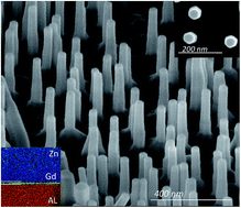
We demonstrate a novel, one-step, catalyst-free method for the production of size-controlled vertical highly conductive ZnO nanorod (NR) arrays with highly desirable characteristics by pulsed laser deposition using a Gd-doped ZnO target. Our study shows that an in situ transparent and conductive Gd nanolayer (with a uniform thickness of ∼1 nm) at the interface between a lattice-matched (11−20) a-sapphire substrate and ZnO is formed during the deposition. This nanolayer significantly induces a relaxation mechanism that controls the dislocation distribution along the growth direction; which consequently improves the formation of homogeneous vertically aligned ZnO NRs. We demonstrate that both the lattice orientation of the substrate and the Gd characteristics are important in enhancing the NR synthesis, and we report precise control of the NR density by changing the oxygen partial pressure. We show that these NRs possess high optical and electrical quality, with a mobility of 177 cm2 (V s)−1, which is comparable to the best-reported mobility of ZnO NRs. Therefore, this new and simple method has significant potential for improving the performance of materials used in a wide range of electronic and optoelectronic applications.


Introduction

Transparent metal oxide nanostructures are promising materials for several potential applications. In particular, the unique optical, electrical, chemical and ferroelectrical properties and multiple functionalities of ZnO nanorods (NRs)1–4 have led many researchers to pursue new synthesis methods with the goal of obtaining high-performance nanoscale devices,3 such as photovoltaic,4–6 field emitters,7,8 solar cells,9–12 sensors,13–15 photoelectrochemical water splitting,16 and nanogenerators.17–19 However, the fabrication of practical ZnO NR-based devices is hindered as controlling the density, shape, size, and growth direction of well-defined vertical ZnO NRs with high conductivity remains a significant challenge.2,3,20–24 Several methods that employed metal catalyst to grow the NRs are avoided due to lack of transparency and metal contamination, which reduces the material efficiency. Therefore, metal catalyst is not suitable for practical devices, especially optoelectronic applications.2,3,20 Moreover, catalyst-free methods employing interfacial textured layers between the NRs and the substrate were not successful in controlling the desired vertical NR structure.25–30 In addition, the interfacial layer should be conductive and transparent for use in optoelectronic devices.26 Consequently, such a layer would be able to, for example, serve as a common electrode to connect NRs with an external circuit of devices.31 Therefore, there still no method that are capable of controlling the structure of well-defined, homogeneous transparent metal oxide NRs for high efficiency devices.

In this work, we present a novel method that allows us to overcome the previously mentioned difficulties, using pulsed laser deposition (PLD). In several studies, PLD systems were used to grow NRs by employing special set-ups that required a priori textured layers25,26,28 and/or a customized high-pressure chamber (a few to several hundred Torr).32–35 However, thus far, none of these PLD methods has been successful.

Our approach enables the production of homogeneous (with respect to height and diameter) arrays of vertical self-assembled hexagonal ZnO NRs grown on transparent substrates using rare earth (RE) dopants. The formation of an in situ homogeneous ultra-thin RE nanolayer (with a uniform well-defined thickness) at the interface between a lattice-matched substrate and the ZnO NRs is the key factor characterizing our approach for obtaining control over the NR structures and their electrical properties. We show that the in situ RE nanolayer assists in producing well-aligned state-of-the-art conductive ZnO NRs with homogeneous heights and sizes. Our method benefits from the use of RE dopants in the RE[thin space (1/6-em)]:[thin space (1/6-em)]ZnO PLD target. In particular, gadolinium (Gd) dopants do not reduce the optical efficiency of ZnO NRs.36

Experimental

Synthesis of ZnO NRs

Gd-doped ZnO laser ablation targets were prepared by mixing 99.75 wt% pure ZnO (99.999%) powder with 0.25 wt% Gd2O3 (99.99%) powder (Sigma-Aldrich-US). A pellet with a diameter of 2.5 cm was pressed and sintered at ∼1100 °C for 12 h to produce a dense, 2.3 cm diameter disc. To grow the ZnO NRs, we used the Gd 0.25 wt% doped ZnO target. A PLD system (Neocera, Pioneer 240) equipped with a krypton fluoride (KrF) excimer laser (λ = 248 nm) was used to ablate the Gd (0.25 wt%) doped ZnO target. The substrate was mounted at a large distance (∼9 cm) vertically above the target, and the vacuum chamber was pumped to 10−6 Torr before target ablation. Next, the growth temperature was set to 650 °C. The ZnO NRs were grown on lattice-matched (11−20) a-Al2O3 by focusing the beam on the Gd-doped ZnO target surface with a beam fluency of 5 ± 0.5 J cm−2. The deposition consisted of 30[thin space (1/6-em)]000 laser pulses delivered at a frequency of 10 Hz. To control the NR density, P(O2) was varied in the range of 15–200 mTorr for all samples. For comparison, Gd-doped ZnO was deposited on (0001) c-Al2O3, while undoped ZnO was deposited on both a-Al2O3 and c-Al2O3 under the same growth conditions.

Characterizations

Morphologies and crystallization were characterized by scanning electron microscopy (SEM) (FEI Nova Nano 630), X-ray diffraction (XRD) (Bruker D8 Discover high resolution XRD with CuKα and λ = 1.5406 Å) and high-resolution transmission electron microscopy (Titan-HRTEM). The electrical properties of our samples were investigated using Hall-effect measurements in a physical property measurement system (PPMS EverCool, Quantum design) by adapting the van der Pauw geometry, with B perpendicular to the direction of the current flow. Photoluminescence (PL) measurements were performed using a 325 nm He–Cd laser with a beam power of ∼8 mW. The samples were mounted in a He closed cycle cryostat system for low-temperature PL measurements (6.5 K). Room temperature (RT) absorption measurements were carried out using UV-vis Varian Cary 5000 spectrophotometry. Cathodoluminescence (CL) maps and secondary electron (SE) images were taken at RT using an FEI Quanta 250 environmental FEGSEM. The electron beam energy was fixed at 5 keV. An Andor spectrograph with a charge coupled device camera was used to detect the spectra.

Results and discussion

Fig. 1 shows SEM images of samples deposited on a-Al2O3 (with a lattice mismatch of 0.08% between (11−20) a-Al2O3 and (0001) ZnO)37 using a Gd-doped ZnO target. Samples prepared at a partial oxygen pressure P(O2) = 15 mTorr are characterized by a continuous film (Fig. 1a). ZnO NRs begin to emerge as P(O2) increases to 25 mTorr (Fig. 1b), whereas low-density ZnO NRs are obtained at P(O2) = 50 mTorr (Fig. 1c). The spacing between these ZnO NRs is well controlled by changing the P(O2). Homogeneous, well-defined, ordered vertical hexagonal ZnO NR arrays are achieved at P(O2) = 100 mTorr (Fig. 1d) and 200 mTorr (Fig. 1e), with average densities of ∼80 and ∼120 NR μm−2, respectively. The NR length is relatively homogeneous (approximately 300 nm). The NR crystalline structure was investigated using high-resolution XRD measurements. Samples deposited at P(O2) = 15 mTorr show strong peaks at 2θ = 34.79° with a full width at half maximum (FWHM) of 0.314°, which corresponds to a (0002) ZnO plane II (11−20) a-Al2O3 substrate, indicating a single crystal film grown along the c-axis (Fig. 1f). We also observed a shift in the (0002) XRD peak of the Gd-doped ZnO film towards higher angles compared to the undoped ZnO film, which was attributed to vacancies accompanying Gd incorporation into the crystal.38 For samples deposited at P(O2) = 50 mTorr, this thin film peak overlaps with the NR peak located at a smaller 2θ = 34.63° (Fig. 1g). As the NR density increases with P(O2), the corresponding XRD peak at 2θ = 34.39° becomes dominant, as shown for samples deposited at P(O2) = 100 and 200 mTorr. The FWHM of the XRD peak of the ZnO NRs is approximately 0.15°, which is comparable to the best value reported for ZnO NRs,39–41 indicating the high crystallinity of these ZnO NRs grown along the c-axis.
image file: c5ra19798h-f1.tif
Fig. 1 SEM images of Gd-doped ZnO samples grown on a-Al2O3 at (a) P(O2) = 15 mTorr, (b) 25 mTorr, (c) 50 mTorr, (d) 100 mTorr, and (e) 200 mTorr. The insets of the (b–e) show the top view. XRD patterns of these Gd-doped ZnO samples; the high angle shoulder represents the XRD peak from the film. The dashed and solid red lines indicate Gaussian fits of the peaks for the NRs and the film, respectively.

To study the effects of substrate mismatch on NR synthesis, we used the same Gd-doped ZnO target to perform deposition at P(O2) = 100 mTorr on a (0001) c-Al2O3 substrate, which has a high lattice mismatch of ∼31.8% with (0001) ZnO,37 for the same deposition conditions of the samples presented in Fig. 1. For this sample, random (rather than well-defined) ZnO NRs are observed, as shown in Fig. 2a. Furthermore, pure ZnO samples were deposited on a-Al2O3 and c-Al2O3 at P(O2) = 100 mTorr to study the effect of Gd doping on the formation of the NRs. Pure ZnO deposited on a-Al2O3 is characterized by a low density of nanocrystals (Fig. 2b), whereas the sample grown on c-Al2O3 shows a continuous film with a rough granular surface morphology (Fig. 2c). Therefore, we conclude that, under particular deposition conditions, both the Gd dopant and the Al2O3 substrate orientation are crucial for the formation of vertical, well-defined, well-ordered ZnO NRs.


image file: c5ra19798h-f2.tif
Fig. 2 SEM images of (a) Gd-doped ZnO on c-Al2O3, (b) undoped ZnO on a-Al2O3, and (c) undoped ZnO on c-Al2O3. All samples were deposited at P(O2) = 100 mTorr.

We observe that the ZnO NR density increases with increasing P(O2). This relationship arises from the correlation between the species energy E and the background pressure PP(O2) in the present case, which is described by42

 
E = Eo[thin space (1/6-em)]exp(−d/λ), (1)
where Eo is the initial energy of the charged species escaping from the target d is the distance between the target and the substrate (∼9 cm). λ is the mean free path of the ablated species (the plasma) traveling towards the substrate in the PLD chamber and can be defined as
 
image file: c5ra19798h-t1.tif(2)
where do is the diameter of the gas molecule, T is the temperature, and k is Boltzmann's constant. Therefore, λ increases with decreasing P, and the kinetic energy of the species on substrate “E” decreases exponentially as P increases, which explains the variation in the NR density with changing pressure. Therefore, at higher P(O2) > 15 mTorr, the ablated species experience a large number of collisions with oxygen molecules, and the condensation of the species on the substrate result in low E that can lead to a Stranski–Krastanov (SK) nucleation and the formation of NRs. At lower P(O2) (<15 mTorr), the ions emitted from the target surface with high E after the laser interaction condense on the substrate surface, that can be high enough to form a continuous film.

Growth mechanism

It is known that structural defects, such as stacking faults, threading dislocations, and grain boundaries, affect the NR growth orientation.24,43–45 Therefore, investigating the structural defects near the interface between the substrate and the Gd-doped ZnO wetting layer is essential for a better understanding of the growth mechanism.44 For this purpose, a cross-section along the c-axis of the NRs sample (Fig. 1c) was analyzed by HRTEM. We observe that the Gd-doped ZnO wetting layer is a single crystal with (0001) growth direction. Moreover, Fig. 3a shows that the value of c lattice parameter is greater (0.54 nm) near the interface compared to that away from the interface (0.52 nm, which is comparable to the c parameter value of bulk ZnO), indicating that the wetting layer is strained near the substrate and starts to relax homogeneously along c-axis as the thickness increases (as shown in the Inverse Fast Fourier Transform (IFFT) (Fig. 3b)). However, no strain is observed along the a-axis, as we find that the value of a parameter (0.325 nm) is similar to that of bulk ZnO, as shown in Fig. 3a and c. Interestingly, although c parameter reaches the ZnO bulk value in a critical thickness, no threading dislocations are observed along c- and a-axis near the substrate interface.
image file: c5ra19798h-f3.tif
Fig. 3 (a) HRTEM image of a vertical cross-section near the interface between substrate and wetting layers. The inset shows the FFT. IFFT (after the masking process by the Digital Micrograph software), (b) from (0002) spots, and (c) from (11−20) spots in the inset of (a) (the red line indicates the interface location).

We investigate chemical compositions near the interface to identify the origin of this uniform strain behavior as the thickness of the wetting layer increases. Energy-dispersive X-ray spectroscopy (EDS) maps of Gd, Zn and Al near the interface are shown in Fig. 4, which confirms that our method enables the formation of an in situ Gd interfacial nanolayer with a uniform ultra-thin thickness of ∼1 nm during deposition. Similarly, electron energy loss spectroscopy (EELS) in different positions near the interface confirms that Gd precipitates near substrate (Fig. S1, ESI,). Forming Gd nanolayer based on the self-purification of ZnO. When impurity solubility is low, and required high energy to be incorporated into the materials, the impurities preferentially defuse to the surface or the interface of materials.46 As Gd concentration increases in the interface, the growth temperature can provide a sufficient energy to Gd atoms in the wetting layer to be diffused near the interface.


image file: c5ra19798h-f4.tif
Fig. 4 EDS maps of Gd-Lα (green), indicating a uniform interfacial Gd layer between the substrate and the ZnO (the green spots shown in the substrate and films are just noise, as signal to noise ratio is extremely low and EDS technique is not sufficiently sensitive to detect such low composition), Zn-Kα (blue), and Al-Kα (red) near the interface.

This diffusion of Gd atoms may occur by different surface diffusion mechanisms.47,48 In PLD, the atoms falling on a substrate have a kinetic energy E obtained in evaporation or ablation processes, as shown in eqn (1). Then these atoms diffuse on the substrate surface. The probability p of an atom jumping from one lattice site to the other one is given by:47,48

 
p = A[thin space (1/6-em)]exp(−Ea/kT), (3)
where A is the hopping rate, Ea is the surface diffusion energy, and T is the substrate temperature, which is a very important parameter of the PLD method.

We believe that this in situ Gd nanolayer acts as a uniform catalyst layer as Gd is metal that assists in forming of Gd-doped ZnO wetting layers with homogenous thickness (Fig. S2, ESI,) and, therefore, uniform nucleation sites, leading to such ZnO NRs. This explains the absence of NRs in undoped ZnO samples grown on either a- or c-Al2O3 substrates.

To investigate the effect of this Gd nanolayer on the strain relaxation mechanism as the thickness of the wetting layer increases and in turn formation of the vertical NRs. Therefore, we study the HRTEM near the interface between the wetting layer and the NR (Fig. 5a). FFT images (Fig. 5b–d) confirm that both the wetting layer and the NR are single crystals with growth along (0001). Edge dislocations (denoted by the symbol “T” in Fig. 5e–j) are observed near the interface between the wetting layer and NR along both c- and a-axis. We find that the density of dislocations along the c-axis (Fig. 5e–g) is greater than that along the a-axis (Fig. 5h–j). Moreover, as the relaxation increases with the wetting layer thickness, the dislocation density near the interface between the NR and the wetting layer increases (Fig. 5e and h), which can be due to a complete strain relaxation.49 However, this density decreases in (Fig. 5f and i) and above the interface (Fig. 5g and j). Remarkably, Fig. 5f and i indicate a rapid reduction in the dislocation density in the interface (see the area circled with yellow in Fig. S3, ESI,) and increases again slightly above the interface in the bottom of the NR. This relaxation mechanism leads to SK nucleation process, which stimulates the growth of homogeneous vertical ZnO NRs with well-defined morphologies. Therefore, at a specific P(O2), we assume that the formation of a uniform in situ Gd nanolayer assists in creating a wetting layer with a homogenous relaxation mechanism to form homogenous ZnO nucleation for vertical orientated NRs.


image file: c5ra19798h-f5.tif
Fig. 5 (a) TEM image near the interface between wetting layers and NR. (b) FFT image from the blue-boxed region in (a), and corresponding IFFT from (e) the (0002) spots and (h) the (11−20) spots in (b). (c) FFT image from the white-boxed region in (a), and corresponding IFFT from (f) the (0002) spots and (i) the (11−20) spots in (c). (d) FFT image from the red-boxed region in (a), and corresponding IFFT from (g) the (0002) spots and (j) the (11−20) spots in (d). (The red line indicates the interface location).

The nucleation is strongly influenced by the surface energy of the free substrate (γs), the interface between the substrate and the wetting layers; in this case, the Gd nanolayer (γi), and the nucleation facet plane (γn) correspond to the minimum surface energy.50 In SK case, the surface energy of the substrate exceeds the combination of both surface energy of interfacial wetting layers and nucleations.50

 
γs > γi + γn. (4)

The same mechanism is employed to explain the absence of ZnO NRs on c-Al2O3. More specifically, no vertical and well defined NRs are observed on the sample deposited on the c-Al2O3 (Fig. 2a) due to a decrease in γs, as the relative surface energies of (11−20) a-Al2O3 and (0001) c-Al2O3 were estimated to be γ(11−20) = 1.12γ(0001).51 Therefore, the a-Al2O3 substrate surface energy and the uniform interfacial Gd nanolayer doping can play a significant role in the growth of high quality vertically aligned hexagonal ZnO NRs.

We can summarize the mechanism of our catalyst-free aligned ZnO NRs, as shown in Fig. 6. The laser beam was focused on a ZnO target doped with Gd to evaporate Zn, O, and Gd atoms. In this arrangement, the P(O2) controls the number of collisions between oxygen molecules and those of the ablated species (Fig. 6 step-I). Fig. 6 step-II shows that the ablated species condense on the above substrate as a wetting layer, forming homogenous in situ Gd nanolayer in the interface near the substrate, due to Gd diffusion. The strain of the witting layer above Gd nanolayer increases with thickness. When the strain of the wetting layer exceeds a critical point, SK nucleation will be formed, decreasing the total strain energy (Fig. 6 step-III). SK nucleation is a favorable site for NRs growth. Our method demonstrated that homogeneous vertical NRs can be grown along the c direction (step-IV) on a transparent in situ Gd layer, without the need for a prefabricated textured or metal catalyst layer.12,29 Moreover, the transparency of samples is not affected by Gd in situ nanolayer, as shown in the photographic image of the 200 mTorr sample (the inset of Fig. 6), indicating its potential use in optoelectronic devices.


image file: c5ra19798h-f6.tif
Fig. 6 Schematic diagram represents the growth mechanism of NRs. The inset is a photographic image of the sample deposited at P(O2) = 200 mTorr (with the highest density of NRs).

In other catalyst-free method that have been previously employed for PLD growth, NRs were produced using customized high gaseous pressure (several Torr) chamber or prefabricated textured layer.25,29,32 High gaseous pressure used during deposition to reduce the kinetic energy of ablated species due to collisions with gas molecules, which leads to the condensation of ablated species and form nanoparticles that act as nucleation sites.32,33,52

Enhancement of the electrical properties of the NRs

The sample deposited at P(O2) = 200 mTorr was selected for further study due to its high NR density. This high density allowed us to obtain ohmic contacts with the NRs after setting them horizontally, as shown in the SEM image (given in the inset of Fig. 7a), on the a-Al2O3 substrate to provide a more accurate estimation of the conductivity and mobility (the scheme in Fig. 7a). Sun et al.53 used the same approach to design a field-effect transistor based on NRs. Therefore, our aim was to measure the overall mobility for applications in various devices. We measured the Hall voltage to estimate the carrier density from the Hall resistance (R). Fig. 7b shows R as a function of the applied magnetic field (B) obtained at different temperatures (T = 10–300 K). R decreases with increasing B, indicating n-type conduction.
image file: c5ra19798h-f7.tif
Fig. 7 (a) Schematic drawing of the Hall measurement contact for a NR sample grown on a-Al2O3 and the corresponding SEM image. (b) Hall measurements at different temperatures and (c) the mobility, carrier concentration and conductivity in the NRs as a function of temperature.

The electron concentration (ne) is calculated from dR/dB by taking into account the NR geometry. Fig. 7c shows the temperature dependence of the conductivity (σe), electron mobility (μe), and ne. The observed variation of σe with temperature indicates semiconducting behavior. ne varies from ∼1–3 × 1019 cm−3 with temperature (T). At RT, the σe and μe values for these NRs are high compared to the previous literature for n-type ZnO NRs,42,54,55 and are estimated to be 855 S cm−1 and 177 cm2 (V s)−1, respectively. The observed high mobility and conductivity can be due to the high crystalline quality of the NRs and the Gd incorporation. Thus, to confirm the effects of the Gd dopants, we performed density functional theory (DFT) calculations for the electronic structure of a wurtzite Zn48O48 NR grown in the (0001) direction with and without Gd doping. To obtain an optimized geometry, the atomic coordinates of the NR were relaxed in both cases. Calculations were performed using the Vienna Ab initio Simulation Package within the generalized gradient approximation (GGA)56,57 and with a plane wave cut-off energy of 400 eV. We employed pseudopotentials based on the projector augmented wave formalism for the spin polarization calculations.58 A 1 × 1 × 8 Monkhorst–Pack k-grid was used to perform the Brillouin zone sampling investigations, using GGA and GGA+U for Gd-doped semiconductor systems yielded very similar results, indicating that the qualitative picture is largely unchanged, and only some minor quantitative differences were detected.59–61 Hence, we do not expect our results to be significantly altered if GGA+U or SIC-LDA is employed to treat the Gd-doped GaN nanowires.

Fig. 8a and b show the band structure (BS) of the pristine ZnO NR and Gd-doped ZnO NR, respectively. The BS is estimated along the Gamma to Z direction, which is parallel to the growth direction of the NR. The NR band gap is calculated to be 1.6 eV, which is greater than that obtained for the bulk ZnO using the GGA due to quantum confinement effects. Qualitatively, the GGA allows for a better understanding of the band structure, even though the experimental value of the band gap is an underestimate. The undoped ZnO NR exhibits semiconducting properties and has a direct band gap at the gamma point, as shown in Fig. 8a. A significant shift in the Fermi level into the conduction band can be observed when Gd dopants are introduced, as shown in Fig. 8b, which explains the high conductivity and mobility of the NRs (in agreement with our experimental findings). Detailed electronic properties are shown elsewhere.62 X-ray absorption spectroscopy found that Gd remains Gd3+ state; whereas Zn atom remains Zn2+ state in Gd doped ZnO samples. Near edge X-ray absorption fine structure spectra at the O K-edge and Gd M5, 4-edges indicated that Gd atoms replace Zn sites.38,63 Therefore, the incorporation of Gd dopants creates a donor band below the conduction band maximum. Due to the donor band created near the CBM, a shift in the Fermi level occurs, and the material conductivity increases. In addition, we observed a strong spin splitting phenomenon.


image file: c5ra19798h-f8.tif
Fig. 8 Calculated band structure of (a) undoped ZnO NRs and (b) Gd-doped ZnO NRs. The Fermi energy is set to zero.

Optical properties of the ZnO NRs

Fig. 9a shows the low temperature PL (6.5 K) of Gd–ZnO films and NRs prepared at P(O2) = 15, 25, 50, 100, and 200 mTorr. The ZnO NRs grown at 200 mTorr show strong and sharp UV near-band-edge (NBE) luminescence caused by the neutral donor-bound exciton (DoX) line at 369.16 nm (3.36 eV), with a narrow FWHM of 7.9 meV. The PL band observed at 3.33 eV is due to donor-to-acceptor (DAP) pair transitions.64 No deep level (DL)-related defects is observed, indicating high optical quality. In particular, the optical efficiency of ZnO is not reduced by Gd incorporation, as the first excitation level of 4f in Gd3+ ion is above the band gap.36 Therefore, no efficient energy can be transferred from electron–hole recombination in ZnO to 4f levels, and therefore, no reduction in bandage emission occurs due to energy transfer.36
image file: c5ra19798h-f9.tif
Fig. 9 (a) PL spectra of ZnO NRs deposited at P(O2) = 15, 25, 50, 100 and 200 mTorr, (b) absorption spectrum of ZnO NRs deposited at P(O2) = 200 mTorr.

The RT absorption measurements were carried out for ZnO NRs grown at P(O2) = 200 mTorr (since this sample exhibits PL dominated by NRs emission) as shown in Fig. 9b. It can be observed that the ZnO NRs band gap is red shifted (∼3.22 eV), compared to bulk ZnO (3.37 eV at RT),65 may be due to tensile stress. The absorption spectrum exhibits step-like character, indicating high crystal quality. A slight tail shown in absorption spectrum might be due to edge dislocations or inhomogeneous strain in the wetting layers.66

RT-CL maps taken in the same area as secondary electron (SE) images are shown in Fig. 10, which allow us to investigate the nanoscale luminescence properties of a single NR.


image file: c5ra19798h-f10.tif
Fig. 10 RT-CL hyperspectral maps (1 × 1 μm) of NRs deposited at 50 mTorr. CL map of (a) the spectral maximum energy (the top left inset presents the corresponding SE images), (b) the NBE emission intensity and (c) the FWHM of the NBE peak.

The CL spectrum can be collected at each point in the map; therefore, the peak fitting allows for an analysis of the spectral parameters, such as the peak energy, width and emission intensity.67 The RT-CL map reveals that the NBE peak position of NRs has a slight redshift (∼3.265 eV) as shown in Fig. 10a compared to that of the bulk ZnO film (3.29 eV),68 which is in good agreement with the absorption measurements.

The peak intensity map (Fig. 10b) and FWHM map (Fig. 10c) demonstrate that the NBE peak of the NRs has a high intensity and a narrow width. In addition, no defect band is observed from RT-CL spectrum of a single NR (Fig. S4, ESI,), demonstrating a high crystalline quality of the NRs, which agrees with low temperature PL.

The advantage of this method is that it allows for deposition of the metal oxide onto a transparent substrate at a suitable temperature based on the surface energy law using RE nanolayer. Although a pre-fabricated seed layer was not used in this work, the resulting NRs were well controlled with good structural, electrical, and optical properties. Therefore, the high electrical and optical quality of these NRS confirm their potential for optoelectronic, photovoltaic and electronic devices.

Conclusions

To the best of our knowledge, we have developed a novel one-step method that demonstrates significant improvements in the formation of homogeneous, ideal, well-ordered vertical NRs on a transparent, conductive, uniform nanolayer without using a pre-fabricated template. The strain relaxation mechanism shows that the dislocation distribution varies as the thickness of the ZnO wetting layer increases and dislocation density declines rapidly in the interface between the ZnO wetting layer and the NRs. This high optical and electrical quality NR structure shows improvement for a wide range of electronic and optoelectronic properties. The mobility observed in the ZnO NRs is comparable with previous reports. We confirm that the lattice-matched a-Al2O3 substrates and the Gd dopants assist in the in situ formation of a uniform Gd interfacial nanolayer, which controls the homogeneity of the ZnO NR structure. This method can be generalized for different oxide materials and for optoelectronic and electronic devices.

Acknowledgements

The authors thank P. Edwards and R. W. Martin for providing access to the CL measurement facility at the University of Strathclyde. We wish to thank Ms Ecaterina Ware from Imperial College London, UK for TEM sample preparation. We acknowledge the financial support from General Directorate of Research Grants, from King Abdul-Aziz City of Science and Technology.

References

  1. U. Ozgur, Y. I. Alivov, C. Liu, A. Teke, M. A. Reshchikov, S. Dogan, V. Avrutin, S. J. Cho and H. Morkoc, J. Appl. Phys., 2005, 98, 041301 CrossRef.
  2. J. L. Gomez and O. Tigli, J. Mater. Sci., 2013, 48, 612–624 CrossRef CAS.
  3. M. Willander, O. Nur, Q. X. Zhao, L. L. Yang, M. Lorenz, B. Q. Cao, J. Z. Perez, C. Czekalla, G. Zimmermann, M. Grundmann, A. Bakin, A. Behrends, M. Al-Suleiman, A. El-Shaer, A. C. Mofor, B. Postels, A. Waag, N. Boukos, A. Travlos, H. S. Kwack, J. Guinard and D. L. Dang, Nanotechnology, 2009, 20, 332001 CrossRef CAS PubMed.
  4. M. Laurenti, G. Canavese, A. Sacco, M. Fontana, K. Bejtka, M. Castellino, C. F. Pirri and V. Cauda, Adv. Mater., 2015, 27, 4218–4223 CrossRef CAS PubMed.
  5. J. Schrier, D. O. Demchenko and L.-W. Wang, Nano Lett., 2007, 7, 2377–2382 CrossRef CAS PubMed.
  6. X.-Y. Chen, T. Ling and X.-W. Du, Nanoscale, 2012, 4, 5602–5607 RSC.
  7. X. D. Wang, J. Zhou, C. S. Lao, J. H. Song, N. S. Xu and Z. L. Wang, Adv. Mater., 2007, 19, 1627–1631 CrossRef CAS.
  8. K. K. Naik, R. Khare, D. Chakravarty, M. A. More, R. Thapa, D. J. Late and C. S. Rout, Appl. Phys. Lett., 2014, 105, 233101 CrossRef.
  9. I. Gonzalez-Valls and M. Lira-Cantu, Energy Environ. Sci., 2009, 2, 19–34 CAS.
  10. C.-H. M. Chuang, P. R. Brown, V. Bulovic and M. G. Bawendi, Nat. Mater., 2014, 13, 796–801 CrossRef CAS PubMed.
  11. Q. Hu, Y. Li, F. Huang, Z. Zhang, K. Ding, M. Wei and Z. Lin, Sci. Rep., 2015, 5, 11499 CrossRef PubMed.
  12. H. Chen, L. Zhu, H. Liu and W. Li, Nanotechnology, 2012, 23, 075402 CrossRef PubMed.
  13. Q. Wan, Q. H. Li, Y. J. Chen, T. H. Wang, X. L. He, J. P. Li and C. L. Lin, Appl. Phys. Lett., 2004, 84, 3654–3656 CrossRef CAS.
  14. X. Xiao, L. Yuan, J. Zhong, T. Ding, Y. Liu, Z. Cai, Y. Rong, H. Han, J. Zhou and Z. L. Wang, Adv. Mater., 2011, 23, 5440–5444 CrossRef CAS PubMed.
  15. M. R. Alenezi, S. J. Henley, N. G. Emerson and S. R. P. Silva, Nanoscale, 2014, 6, 235–247 RSC.
  16. H. Chen, Z. Wei, K. Yan, Y. Bai, Z. Zhu, T. Zhang and S. Yang, Small, 2014, 10, 4760–4769 CrossRef CAS PubMed.
  17. Z. L. Wang and J. H. Song, Science, 2006, 312, 242–246 CrossRef CAS PubMed.
  18. M. K. Gupta, J.-H. Lee, K. Y. Lee and S.-W. Kim, ACS Nano, 2013, 7, 8932–8939 CrossRef CAS PubMed.
  19. G. Nagaraju, Y. H. Ko and J. S. Yu, Mater. Chem. Phys., 2015, 149, 393–399 CrossRef.
  20. S. Wang, C. Song, K. Cheng, S. Dai, Y. Zhang and Z. Du, Nanoscale Res. Lett., 2012, 7, 246 CrossRef PubMed.
  21. T. Ngo-Duc, K. Singh, M. Meyyappan and M. M. Oye, Nanotechnology, 2012, 23, 194015 CrossRef PubMed.
  22. R. Zhu, W. G. Zhang, C. Li and R. S. Yang, Nano Lett., 2013, 13, 5171–5176 CrossRef CAS PubMed.
  23. J. Joo, B. Y. Chow, M. Prakash, E. S. Boyden and J. M. Jacobson, Nat. Mater., 2011, 10, 596–601 CrossRef CAS PubMed.
  24. D. Tsivion, M. Schvartzman, R. Popovitz-Biro, P. von Huth and E. Joselevich, Science, 2011, 333, 1003–1007 CrossRef CAS PubMed.
  25. S. S. Lin, J. I. Hong, J. H. Song, Y. Zhu, H. P. He, Z. Xu, Y. G. Wei, Y. Ding, R. L. Snyder and Z. L. Wang, Nano Lett., 2009, 9, 3877–3882 CrossRef CAS PubMed.
  26. J. P. Kar, J.-H. Choi, S. N. Das, J. Xiong, M.-J. Lee, T. I. Lee and J.-M. Myoung, J. Nanosci. Nanotechnol., 2011, 11, 2185–2190 CrossRef CAS PubMed.
  27. C. V. Varanasi, K. D. Leedy, D. H. Tomich, G. Subramanyam and D. C. Look, Nanotechnology, 2009, 20, 385706 CrossRef CAS PubMed.
  28. D. Yu, L. Hu, J. Li, H. Hu, H. Zhang, Z. Zhao and Q. Fu, Mater. Lett., 2008, 62, 4063–4065 CrossRef CAS.
  29. J.-I. Hong, J. Bae, Z. L. Wang and R. L. Snyder, Nanotechnology, 2009, 20, 085609 CrossRef PubMed.
  30. L. E. Greene, M. Law, D. H. Tan, M. Montano, J. Goldberger, G. Somorjai and P. D. Yang, Nano Lett., 2005, 5, 1231–1236 CrossRef CAS PubMed.
  31. X. Wang, J. Song, J. Liu and Z. L. Wang, Science, 2007, 316, 102–105 CrossRef CAS PubMed.
  32. T. Premkumar, Y. S. Zhou, Y. F. Lu and K. Baskar, ACS Appl. Mater. Interfaces, 2010, 2, 2863–2869 CAS.
  33. R. Q. Guo, J. Nishimura, M. Matsumoto, D. Nakamura and T. Okada, Appl. Phys. A: Mater. Sci. Process., 2008, 93, 843–847 CrossRef CAS.
  34. A. Rahm, M. Lorenz, T. Nobis, G. Zimmermann, M. Grundmann, B. Fuhrmann and F. Syrowatka, Appl. Phys. A: Mater. Sci. Process., 2007, 88, 31–34 CrossRef CAS.
  35. M. Lorenz, E. M. Kaidashev, A. Rahm, T. Nobis, J. Lenzner, G. Wagner, D. Spemann, H. Hochmuth and M. Grundmann, Appl. Phys. Lett., 2005, 86, 143113 CrossRef.
  36. J. M. Zavada, N. Nepal, J. Y. Lin, H. X. Jiang, E. Brown, U. Hommerich, J. Hite, G. T. Thaler, C. R. Abernathy, S. J. Pearton and R. Gwilliam, Appl. Phys. Lett., 2006, 89, 152107 CrossRef.
  37. P. Fons, K. Iwata, A. Yamada, K. Matsubara, S. Niki, K. Nakahara, T. Tanabe and H. Takasu, Appl. Phys. Lett., 2000, 77, 1801–1803 CrossRef CAS.
  38. M. Subramanian, P. Thakur, M. Tanemura, T. Hihara, V. Ganesan, T. Soga, K. H. Chae, R. Jayavel and T. Jimbo, J. Appl. Phys., 2010, 108, 053904 CrossRef.
  39. Q. Li, K. Gao, Z. Hu, W. Yu, N. Xu, J. Sun and J. Wu, J. Phys. Chem. C, 2012, 116, 2330–2335 CAS.
  40. Y. Sun, G. M. Fuge and M. N. R. Ashfold, Chem. Phys. Lett., 2004, 396, 21–26 CrossRef CAS.
  41. S. S. Kim and B. T. Lee, Thin Solid Films, 2004, 446, 307–312 CrossRef CAS.
  42. M. Yan, H. T. Zhang, E. J. Widjaja and R. P. H. Chang, J. Appl. Phys., 2003, 94, 5240–5246 CrossRef CAS.
  43. E. Uccelli, J. Arbiol, C. Magen, P. Krogstrup, E. Russo-Averchi, M. Heiss, G. Mugny, F. Morier-Genoud, J. Nygard, J. R. Morante and A. F. I. Morral, Nano Lett., 2011, 11, 3827–3832 CrossRef CAS PubMed.
  44. H. Chen, J. Luo, T. Zeng, L. Jiang, Y. Sun, Z. Jiao, Y. Jin and X. Sun, New J. Chem., 2014, 38, 3907–3916 RSC.
  45. R. L. Penn and J. F. Banfield, Science, 1998, 281, 969–971 CrossRef CAS PubMed.
  46. G. M. Dalpian and J. R. Chelikowsky, Phys. Rev. Lett., 2006, 96, 226802 CrossRef PubMed.
  47. L. Pyziak, W. Obermayr, K. Zembrowska and M. Kuzma, Semicond. Phys., Quantum Electron. Optoelectron., 2003, 6, 183–188 CAS.
  48. Z. Y. Zhang and M. G. Lagally, Science, 1997, 276, 377–383 CrossRef CAS PubMed.
  49. A. P. Payne, W. D. Nix, B. M. Lairson and B. M. Clemens, Phys. Rev. B: Condens. Matter Mater. Phys., 1993, 47, 13730–13736 CrossRef CAS.
  50. G. Cao, Nanostructures & Nanomaterials Synthesis, properties, & application, Imperial college press, London, 2004 Search PubMed.
  51. J. H. Choi, D. Y. Kim, B. J. Hockey, S. M. Wiederhorn, J. E. Blendell and C. A. Handwerker, J. Am. Ceram. Soc., 2002, 85, 1841–1844 CrossRef CAS.
  52. M. Kawakami, A. B. Hartanto, Y. Nakata and T. Okada, Jpn. J. Appl. Phys., Part 2, 2003, 42, L33–L35 CrossRef CAS.
  53. B. Sun and H. Sirringhaus, Nano Lett., 2005, 5, 2408–2413 CrossRef CAS PubMed.
  54. W. Liang, B. D. Yuhas and P. Yang, Nano Lett., 2009, 9, 892–896 CrossRef CAS PubMed.
  55. N. A. Jayah, H. Yahaya, M. R. Mahmood, T. Terasako, K. Yasui and A. M. Hashim, Nanoscale Res. Lett., 2015, 10, 7 CrossRef PubMed.
  56. G. Kresse and J. Hafner, Phys. Rev. B: Condens. Matter Mater. Phys., 1993, 47, 558–561 CrossRef CAS.
  57. G. Kresse and J. Furthmuller, Phys. Rev. B: Condens. Matter Mater. Phys., 1996, 54, 11169–11186 CrossRef CAS.
  58. J. P. Perdew, K. Burke and M. Ernzerhof, Phys. Rev. Lett., 1996, 77, 3865–3868 CrossRef CAS PubMed.
  59. H. Shi, P. Zhang, S.-S. Li and J.-B. Xia, J. Appl. Phys., 2009, 106, 023910 CrossRef.
  60. Y. Li, R. Deng, W. Lin, Y. Tian, H. Peng, J. Yi, B. Yao and T. Wu, Phys. Rev. B: Condens. Matter Mater. Phys., 2013, 87, 155151 CrossRef.
  61. G. M. Dalpian and S. H. Wei, Phys. Rev. B: Condens. Matter Mater. Phys., 2005, 72 Search PubMed.
  62. S. A. Aravindh, U. Schwingenschloegl and I. S. Roqan, J. Appl. Phys., 2014, 116, 233906 CrossRef.
  63. S. Venkatesh, J. B. Franklin, M. P. Ryan, J. S. Lee, H. Ohldag, M. A. McLachlan, N. M. Alford and I. S. Roqan, J. Appl. Phys., 2015, 117, 013913 CrossRef.
  64. B. P. Zhang, N. T. Binh, Y. Segawa, K. Wakatsuki and N. Usami, Appl. Phys. Lett., 2003, 83, 1635–1637 CrossRef CAS.
  65. A. Janotti and C. G. Van de Walle, Rep. Prog. Phys., 2009, 72, 126501 CrossRef.
  66. A. Cremades, L. Gorgens, O. Ambacher, M. Stutzmann and F. Scholz, Phys. Rev. B: Condens. Matter Mater. Phys., 2000, 61, 2812–2818 CrossRef CAS.
  67. P. R. Edwards, L. K. Jagadamma, J. Bruckbauer, C. Liu, P. Shields, D. Allsopp, T. Wang and R. W. Martin, Microsc. Microanal., 2012, 18, 1212–1219 CrossRef CAS PubMed.
  68. Y. F. Chen, D. M. Bagnall, H. J. Koh, K. T. Park, K. Hiraga, Z. Q. Zhu and T. Yao, J. Appl. Phys., 1998, 84, 3912–3918 CrossRef CAS.

Footnote

Electronic supplementary information (ESI) available. See DOI: 10.1039/c5ra19798h

This journal is © The Royal Society of Chemistry 2015
Click here to see how this site uses Cookies. View our privacy policy here.