DOI:
10.1039/C5RA14595C
(Paper)
RSC Adv., 2015,
5, 84295-84302
Synthesis and characterization of earth-abundant Cu2MnSnS4 thin films using a non-toxic solution-based technique
Received
23rd July 2015
, Accepted 28th September 2015
First published on 28th September 2015
Abstract
Earth-abundant Cu2MnSnS4 (CMTS) thin films were fabricated through a non-toxic spin-coating technique. The precursor solution is based on a 2-methoxyethanol solvated thiourea complex with acetyl-acetone used as an additive agent, and the spin-coated films were post-annealed at 570 °C under a N2 atmosphere. The influence of annealing time on the structure, composition, morphology, and optical properties of the processed precursor films has been studied in detail. We found that a longer annealing time during CMTS growth can improve the phase purity, promote the preferred orientation along the (112) direction, and enhance grain growth in the micrometer range. Film annealed for 10 min gives a pure CMTS phase, whereas other films annealed for lower and/or higher than 10 min (especially 13 min) can form secondary phases (i.e., SnS, MnS). The band gap energy is estimated as 1.63–1.18 eV for post-annealed films depending on the heat treatment, compared to 1.69 eV for as-prepared film. An efficiency of 0.49% for the device fabricated here has been achieved with an open-circuit voltage of 308.4 mV, a short-circuit current density of 4.7 mA cm−2, and a fill factor of 33.9%. It offers a new research direction for the application of a CMTS absorber layer in low-cost solar cells.
1. Introduction
Thin film solar cells based on Cu(In,Ga)S2 (CIGS) have reached a high level of photoelectric conversion efficiency (over 20%).1 However, gallium and indium which are used for preparation of the absorber layer are very rare and unceasingly used in many industries, which could lead to a shortage in the supply of these elements and contributes to the high fabrication costs of CIGS solar cells.2 Related to the quaternary chalcogenide Cu2ZnSnS4 (CZTS), the naturally occurring mineral Cu2MnSnS4 (CMTS) has a direct band gap energy of 1.0–1.4 eV and a large absorption coefficient of over 104 cm−1, properties that are similar to those of CIGS, which is regarded as one of the potential absorber materials for sustainable and highly efficient solar cells.3–5 Moreover, compared to CIGS, CMTS consists of abundant and inexpensive Mn and Sn that are advantageous for the realization of low-cost solar cells.
Typically, quaternary chalcogenide films such as CIGS and CZTS are deposited using evaporation or sputtering techniques that rely on the use of environments which are under vacuum.6–8 However, these processes suffer from low throughput and difficulties associated with large scale production. In consideration of this, different kinds of solution-based approaches have been developed for the synthesis of Cu-based films such as hot-injection,5,9 solvothermal,10 hydrazine-based approach11,12 and sol–gel spin-coating methods.13–18 Additionally, hot-injection and solvothermal methods have been employed for the synthesis of CMTS nanoparticles,5,10 but there are some limitations. In the hot-injection method, precursors are injected into a hot organic medium to instigate the synthesis process. The solvothermal method also requires a complex reactor autoclave to achieve high pressures for the chemical reactions to proceed. Currently, the record efficiency for CZTSSe devices was obtained through spin-coating a hydrazine-based ink followed by fast annealing.12 However, hydrazine is very unstable and highly toxic which requires extreme caution in handling and storage. Among the solution methods typically used, the spin-coating method is a very simple and low-cost process based on hydrolysis and poly-condensation reactions.14,16 With this in mind, developing a simple, low-cost and non-toxic spin-coating method is highly desirable for the fabrication of high quality and single phase CMTS materials, which is critical to meet the requirements of photovoltaic technologies.
In the present work, we have developed a non-toxic and simple process using a simple solution-based spin-coating method. Conventional aqueous sol–gel processes entail the formation of metal–O–metal bonds in the precursor solution or during the annealing step, which can lead to the formation of secondary phases such as binary sulfides (Cu2−xS) and oxides (SnO2), and has a limitation in terms of heat treatment at high temperature.13,19 As for the formation of sulfides through a sol–gel technique, the process is generally highly active, but toxic hydrogen sulfide gas is used in sulfurizing oxides into sulfides, which makes the prepared thin films not only contain secondary phases, but also show poor surface morphology and weak adhesion to substrates.15 Here, 2-methoxyethanol was used as solvent, and thiourea (TU) was utilized to form metal–TU complexes. As previously reported, in aqueous and/or organic solvents, metal–TU and/or M–TU–M complexes are easily generated.14 In order to increase the solubility of the precursors and improve the adhesion of the precursor films during the condensation reaction, acetyl-acetone was added as an additive agent. Previously, we have reported that a bi-layered structure (a large grain top layer and a small-grain bottom layer) is easily formed in a CZTS-based solar cell processed with a longer deposition time,20 which can be due to the fact that sulfur is hardly incorporated into the relatively thick CZTS layers. Therefore, rapid thermal processing without sulfurization is utilized to fabricate CMTS films to avoid the formation of a bi-layered structure and the influence of post-annealing time on the structural, compositional, morphological and optical properties of the synthesized CMTS thin films was systematically investigated. Also, for the first time we have demonstrated the fabrication of CMTS solar cells with a conversion efficiency of 0.49%, based on this spin-coating method.
2. Experimental
2.1 Precursor solution preparation
All chemicals were purchased from Sigma-Aldrich and used as received. In a typical synthesis, CuCl2·2H2O (7.04 mmol, 99.0%), SnCl2·2H2O (4.0 mmol, 98.0%), and Mn(CH3COO)2·4H2O (4.8 mmol, 99.0%) were used as precursor materials dissolved in 2-methoxyethanol (20 ml, 99.8%) using a magnetic stirrer. Subsequently, thiourea (32 mmol, 99.0%), chosen as the sulfur source, was added. Then, a few drops of acetyl-acetone (99.0%) were added as an additive. The final solution was stirred for 30 min at 50 °C to yield a homogeneous, clear and transparent solution. The chemical composition ratios of the raw materials were controlled to have the atomic ratio of Mn/Sn = 1.2 and Cu/(Mn + Sn) = 0.8. This solution was stable for several months.
2.2 Film preparation
CMTS films were deposited via spin-coating the prepared transparent solution on Mo-coated soda-lime glass (SLG) substrates at 3000 rpm for 30 s followed by a pre-annealing process at 300 °C for 3 min. To reach the targeted thickness of the absorber layer, the spin-coating and pre-annealing processes were repeated twelve times. Finally, the post-annealing temperature was fixed at 570 °C under a N2 gas flow at a heating rate of 8 °C s−1, and then the samples were cooled naturally to room temperature. The film processing sequence is presented in Fig. 1a. In order to investigate the effect of the post-annealing time on the growth of the CMTS films, samples 1–5 were prepared with heat preservation times of 1, 4, 7, 10 and 13 min, the temperature profile for which is shown in Fig. 1b. The as-prepared and post-annealed CMTS films with times of 1, 4, 7, 10, and 13 min were designated as CMTS-00, CMTS-01, CMTS-04, CMTS-07, CMTS-10 and CMTS-13, respectively, where the numbers represent the various annealing times.
 |
| | Fig. 1 (a) Schematic diagram of the CMTS film fabrication sequence, (b) post-annealing temperature profile. | |
2.3 Device fabrication
The completed CMTS solar cell devices with the commonly employed structure of AZO/i-ZnO/CdS/CZTS/Mo/glass were prepared in the present study.13 The CdS buffer layer with approximately a 50–60 nm thickness was grown through chemical bath deposition from an aqueous solution of CdSO4 (1.5 mmol, 99.0%), thiourea (75 mmol, 99.0%) and ammonia (1.8 mmol) at 80 °C. Then window layers of undoped zinc oxide of about 50 nm thickness and Al-doped ZnO (AZO) of approximately 600 nm thickness were deposited through radio-frequency (RF) magnetron sputtering. Finally, a mechanical scribing step was performed to define the cell area as 0.16 cm2.
2.4 Characterization
The coating solution was examined via thermogravimetric analysis (TGA, TA Instrument Q50) under a nitrogen atmosphere. The crystalline structures of the as-prepared and post-annealed CMTS films were identified through X-ray diffraction (XRD) using a Bruker D8 Discover diffractometer with Cu Kα radiation (λ = 1.54056 Å) from 10° to 70°. The tube voltage and current for the XRD patterns were 40 kV and 40 mA, respectively. Raman scattering experiments were performed with a micro-Raman spectrometer (Jobin-Yvon LabRAM HR 800UV). The morphologies and the chemical composition were characterized using a field emission scanning electronic microscope (SEM, FEI, S-4700) attached to an energy-dispersive X-ray spectroscope (EDS). The optical properties were determined using transmittance spectra (UV/vis Lambda 2S, Perkin-Elmer). Current–voltage characteristics of the devices were measured under an AM 1.5 global spectrum with the irradiance set to 100 mW cm−2. All measurements were performed at room temperature.
3. Results and discussion
3.1 Synthesis mechanism
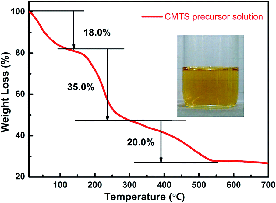
The possible mechanism for the synthesis of the CMTS precursor complex using the current solution route is as follows. In the solution preparation, firstly, metal salts were added into 2-methoxyethanol, Sn2+ ions are oxidized to Sn4+ by Cu2+, corresponding to eqn (1). Concurrently, when the TU was added to the solvent, a transparent solution was formed (shown in the inset of Fig. 2) under magnetic stirring for several minutes, which confirms the formation of metal–TU complexes (Cu–Tu, Mn–Tu, and Sn–Tu). Finally, Cu+, Mn2+, Sn4+, and S2− ions in the homogenous solution organize themselves to form the precursor complex. The detailed reaction equations are as follows:| | |
2Cu2+ + Sn2+ → 2Cu+ + Sn4+
| (1) |
| | |
Cu+ + nTU → [Cu(TU)n]+
| (2) |
| | |
Sn4+ + nTU → [Sn(TU)n]4+
| (3) |
| | |
Mn2+ + nTU → [Mn(TU)n]2+
| (4) |
| | |
[Cu(TU)n]+ + [Mn(TU)n]2+ + [Sn(TU)n]4+ → [CuMnSn(TU)n]m+
| (5) |
 |
| | Fig. 2 Thermo-gravimetric analysis of the CMTS precursor solution. Inset shows the prepared homogeneous CMTS solution. | |
Generally, sol films could be obtained through spin-coating the produced solution. Subsequently, the sol film was pre-annealed in order to remove organic residues and obtain a dense precursor film. Decomposition of the thiourea–metal complexes and the formation of CMTS are involved in this process. In order to gain the decomposition data, the obtained homogenous CMTS precursor solution, as presented in the inset of Fig. 2, was dried at 70 °C for several days and the obtained powder was subjected to TGA. The TGA data in Fig. 2 exhibits a first weight loss stage from room temperature to 140 °C, indicating the thermal evaporation of solvent and water. The second region starts at 140 °C and persists until 300 °C leading to about a 35.0% loss in weight due to thermal decomposition of the metal–TU complex and excess thiourea. At 300 °C, the formation of the CMTS compound is almost completed, and consequently the weight loss rate reduces thereafter. The weight loss still continues at a lower rate beyond 300 °C which may be due to the decomposition of residual precursor and other volatile organic moieties.21 It is also noteworthy that the TGA spectrum obtained in this work is similar to those reported for CZTS solutions prepared using the same solvent.13 Based on the above results, we estimate that the pre-annealed temperature required to remove the solvent and other volatile moieties from the precursor and achieve complete thermal decomposition of the metal–thiourea complexes during the spin coating process must be above 300 °C.
3.2 Structural studies
3.2.1 XRD characterization. The phase evolution of the CMTS precursor during annealing is presented in Fig. 3a. It can be seen that the as-prepared and post-annealed films with low annealing time (<4 min) show a weak and broad peak at 2θ ≈ 28.21°. Apart from the broad and less intense peak, the S phase (PDF: 65-1101; marked with ●) are detected in CMTS-00 before annealing. For sample CMTS-01, the S phase is not visible anymore and an amorphous CMTS phase is formed, which demonstrates that a short annealing time is insufficient for a complete reaction. Upon increasing the annealing time to 4 min, a considerable sharpening in the main diffraction peaks occurs, exhibiting that the CMTS phase could become the predominant phase in these conditions. Sharp peaks at 2θ ≈ 18.02°, 28.21° and 46.99° can be indexed to the diffraction of the (101), (112), and (220)/(204) planes of stannite CMTS (PDF: 51-0757), respectively. As the annealing time increases to 7 min, the (112) peak shows a dramatic increase, and the other diffraction peaks are well defined without additional impurity peaks, suggesting that the as-prepared films could be completely annealed into CMTS at the present conditions. No obvious impurity phase could be observed and the relatively intensity of the (112) plane shows a slight increment for CMTS-10, as shown in Fig. 3b, which presents the enlarged 2θ range from 27.7° to 29.7° of the (112) peak of the CMTS films. The (112) peak intensity decreases as the annealing time is further increased to 13 min. The decrease of the (112) peak intensity indicates that when the annealing time is too long it leads to decline of the CMTS crystallinity. Additionally, there are diffraction peaks of secondary phases at 2θ ≈ 26.53° and 34.31° (marked with ♦ and #) that can be attributed to the Cu4SnS4 (PDF: 27-0196) and MnS (PDF: 06-0815) phases, respectively, which indicates that further prolonging the annealing time may lead to the decomposition of CMTS films.
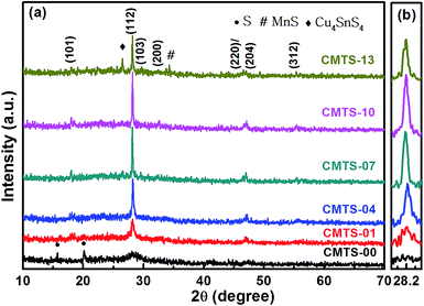 |
| | Fig. 3 (a) XRD patterns of the CMTS films prepared at different annealing times; (b) the magnified pattern of the (112) peak for a 2θ range from 27.7° to 29.7°. | |
The full-width at half-maximum (FWHM) of the (112) peak was measured and is summarised in Table 1. As presented in Table 1, the FWHM decreases from 0.481 to 0.169° as the annealing time increases from 1 min to 10 min, and then slightly increases to 0.174° with further prolonging the annealing time to 13 min. It should be noted that structural defects, internal strain and crystallite sizes can be correlated to the widths of the diffraction peaks. The interplanar spacing of the post-annealed films increases with the increase in annealing time, which indicates the internal compressive strain relaxation in CMTS films.4 Structural defects generally refer to dislocation density and local inhomogeneity etc. in polycrystalline to crystal materials. As shown in Fig. 5, the composition of all of the CMTS samples deviates from the stoichiometry of Cu2MnSnS4, which implies that structural defects might exist. Moreover, the crystallite size (CS) values of these samples have been calculated using Scherrer’s equation D = 0.9λ/(β![[thin space (1/6-em)]](https://www.rsc.org/images/entities/char_2009.gif) cosθ).13 The CS rises significantly from 16.84 to 48.19 nm with increasing the annealing time to 10 min and thereafter it decreases to 46.82 nm due to the degradation of the CMTS phase. The dislocation density (δ) values, defined as the length of dislocation lines per unit volume (lines per m2), can be obtained from the Williamson–Smallman’s formula, δ = 1/D2.22 The tendency of δ to decrease, as presented in Table 1, demonstrates that samples annealed for a shorter time have more crystal defects. Moreover, the lattice parameters (i.e. a and c) were calculated in accordance with the Bragg equation.23 The lattice constant a decreases with the increase of the annealing time, whereas c shows a tendency to increase. Furthermore, the calculated crystal parameters for the film annealed at 10 min are in good agreement with the reported values.24
cosθ).13 The CS rises significantly from 16.84 to 48.19 nm with increasing the annealing time to 10 min and thereafter it decreases to 46.82 nm due to the degradation of the CMTS phase. The dislocation density (δ) values, defined as the length of dislocation lines per unit volume (lines per m2), can be obtained from the Williamson–Smallman’s formula, δ = 1/D2.22 The tendency of δ to decrease, as presented in Table 1, demonstrates that samples annealed for a shorter time have more crystal defects. Moreover, the lattice parameters (i.e. a and c) were calculated in accordance with the Bragg equation.23 The lattice constant a decreases with the increase of the annealing time, whereas c shows a tendency to increase. Furthermore, the calculated crystal parameters for the film annealed at 10 min are in good agreement with the reported values.24
Table 1 Lattice constants of the CMTS films obtained from XRD patterns
| Sample ID |
FWHM of the (112) peak (degree) |
Interplanar spacing of (112) (Å) |
Lattice constant a (Å) |
Lattice constant c (Å) |
Volume of crystal (Å3) |
Crystallite size D (nm) |
Dislocation density δ (lines per m2) |
| CMTS-01 |
0.481 |
3.152 |
5.58 |
10.48 |
326.31 |
16.84 |
35.3 × 10¹⁴ |
| CMTS-04 |
0.215 |
3.157 |
5.55 |
10.63 |
327.43 |
37.68 |
7.04 × 10¹⁴ |
| CMTS-07 |
0.172 |
3.163 |
5.52 |
10.80 |
329.08 |
47.09 |
4.02 × 10¹⁴ |
| CMTS-10 |
0.153 |
3.165 |
5.54 |
10.70 |
328.40 |
51.94 |
3.57 × 10¹⁴ |
| CMTS-13 |
0.174 |
3.163 |
5.54 |
10.72 |
329.01 |
46.82 |
4.51 × 10¹⁴ |
3.2.2 Raman spectroscopy. It is observed that the 2θ positions of the dominant peak of CMTS and Cu2SnS3 (CTS) are very close,23 which makes it difficult to confirm the CMTS phase from XRD pattern analysis. Therefore, Raman spectroscopy was utilized to obtain further insight into the phase identification. The results of the CMTS films as a function of the annealing time are shown in Fig. 4. The as-prepared precursor film exhibits a broad band which encompasses the main modes expected from CMTS and/or CTS. According to the results of the TGA, at 300 °C, the formation of the CMTS compound is almost completed. Therefore, it might be inferred that the broad band can simply be ascribed to CMTS, but with poor crystallinity. The sample taken at 1 min shows a strong peak positioned at ∼328 cm−1, which is attributed to the A1 mode of CMTS. The A1 mode in CMTS involves only the anion vibrations and it has been assigned to the most intense lines observed in the experimental Raman spectra.25 With increasing the annealing time to 4 min, more characteristic peaks of CMTS are resolved. However, the CMTS-04 sample also exhibits a weak peak at 292 cm−1 which can be assigned to the MnS impurity phase.26 For the CMTS-07 film, there is a major peak positioned at 327 cm−1, along with two weak peaks at 245 cm−1 and 345 cm−1, which are consistent with previously reported CMTS values.23 The film annealed for 10 min appears similar to that which was annealed for 7 min. No evidence of other possible binary phases appears in the CMTS-10 Raman spectrum, indicating that the pure CMTS phase has been obtained. Moreover, there are no visible peaks which could be attributed to CTS since the characteristic peaks at 260, 298, and 356 cm−1 could not be observed.7,13,27 However, the CMTS-13 sample shows additional peaks at 217 and 292 cm−1 which can be assigned to the SnS and MnS phases, respectively. A weak peak appears at 474 cm−1 indicating the presence of the Cu2−xS phase.28 The SnS phase observed in CMTS-13 is not detected in the XRD pattern, which is possibly due to only a small amount of the SnS phase existing.
 |
| | Fig. 4 Room temperature Raman spectra of (a) CMTS-00, (b) CMTS-01, (c) CMTS-04, (d) CMTS-7, (e) CMTS-10, and (f) CMTS-13. Inset is the FWHM and peak position of the main A1 mode of the CMTS films. | |
The effect of annealing time on the CMTS films can be better understood by comparing the FWHM values of the dominant A1 mode, since the sharpness of the A1 mode can reflect the crystalline quality of films.29 For all of the post-annealed films, the FWHM values for the main A1 mode was measured and is presented in the inset of Fig. 4. The variation of the FWHM of the A1 mode with the change in annealing time is distributed from 12.95 to 7.85 cm−1. In particular, the minimum FWHM, 7.85 cm−1, is for the film annealed for 10 min which represents the best crystallinity. Moreover, the main peak position shows a small red-shift with an increase of the annealing time and then shifts towards high wavenumbers upon further increase of the annealing time to 13 min, which could be related to the presence of impurity phases and/or stress.30 The present experimental results display that further prolonging the annealing time up to 13 min could lead to decomposition of the CMTS phase. Therefore, the annealing time is very important for modulation of the secondary phase and fabrication of high quality CMTS films.
3.3 Composition analysis
The elemental compositions and compositional ratios of the as-prepared and post-annealed CMTS thin films are presented in Fig. 5. In the annealing time range studied, a general upward trend in the Cu content is observed. The ratio of Cu/(Mn + Sn) exhibits a similar trend as well. The ratio of Mn and Sn seems to be fluctuating which may be due to the evaporation of some components in the form of chalcogenide during annealing at a high temperature (570 °C). It has been reported that Sn is easily lost in the SnS phase at annealing temperatures higher than 400 °C.28 Further studies are still needed regarding the chemical kinetics of this material to obtain stability of the cation stoichiometry. In addition, a dramatic decrease of the S/metal ratio (from 0.81 to 0.68) and an increase of the Cu/(Mn + Sn) ratio (from 0.91 to 2.21) can be observed from Fig. 5b with the post-annealing time ranging from zero to 13 min, which may arise from the decomposition of the CMTS phase and volatilization of S during the long annealing process. Specifically the post-annealing process may give rise to the S-poor state, which may be fine-tuned by increasing the molar concentration of TU incorporated in the solution preparation (eqn (2)–(4)). The decomposition of the CMTS annealed for 13 min has been confirmed through XRD and Raman measurements.
 |
| | Fig. 5 (a) Chemical composition and (b) composition ratios of the precursor and sulfurized CMTS thin films. | |
3.4 Film morphology
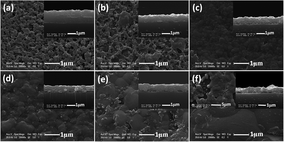
Fig. 6 shows the SEM images of the as-prepared precursor and of the films obtained at various annealing times. It can be seen that the as-prepared granular film has a cracked structure with a particle size smaller than 100 nm. This is consistent with the broad XRD peaks. The resultant grain size is increased with increasing the annealing time. Upon post-annealing for 1 min at 570 °C, parts of the small nanoparticles generated grew into large clusters of particles, as shown in Fig. 6b. The porosity (number of voids) of the film decreases sharply with increasing the annealing time to 4 min. Moreover, a relatively dense structure with large grains (∼500 nm) and occasional voids developed when the annealing time was 4 min. As the annealing time further increase to 10 min, the film exhibits a more uniform and compact surface and a relative enlargement in the grain size can be observed. The smeared and unsmooth surface could be caused by bad cutting. As shown in Fig. 6f, the grain size increased to 2 μm as the annealing time was increased to 13 min, however, the film also exhibits large voids and porous structures (the inset of Fig. 6f gives an enlarged section image of the CMTS-13 surface). The appearance of the poor surface of CMTS-13 could be due to overgrowth of the grains which has been confirmed through XRD and Raman results.
 |
| | Fig. 6 Surface and cross-sectional SEM images of (a) CMTS-00, (b) CMTS-01, (c) CMTS-04, (d) CMTS-07, (e) CMTS-10, and (f) CMTS-13. The insets show the cross-section SEM micrographs of those samples. | |
The insets in Fig. 6 show the cross-section SEM micrographs of those samples. As presented in the inset of Fig. 6a, the as-prepared precursor film shows a thickness of around 1.9 μm and the other post-annealed thin films show film thicknesses of ∼1.2 μm. As can be observed, the film thickness decreases dramatically for the precursor films which were post-annealed. We have reported previously that post-annealing the precursor film would lead to improvement of the crystal quality and a decrease in thickness due to decomposition and crystallization processes.4 Additionally, the films prepared at longer annealing times (7, 10, and 13 min) have some grains extending from the bottom to the top of the CMTS layer without large numbers of voids, relevant to the slight Sn loss during the annealing process, which would lead to the voids at the grain boundaries and/or CMTS/SLG interface.31 The film annealed for 13 min shows large grains that extend through the film and large voids at the CMTS/SLG interface. Even though the films consist of voids at the interface the overall adhesion of the film is good enough.
3.5 Optical properties
The optical transmittance spectra of the CMTS thin films prepared with different annealing times were measured for the determination of the band gap (Eg). According to the transmittance spectra, the optical absorption coefficient α is calculated using the equation α = −ln(T)/t, where T is the transmittance of the film and t is the film thickness. The Eg of CMTS can be determined by applying the equation (αhν)2 = A(hν − Eg).32 The optical band gap is determined by extrapolating the linear region of the plot (αhν)2 vs. hν and taking the intercept on the horizontal photon energy axis.
The typical (αhν)2 vs. hν plots of CMTS thin films are presented in Fig. 7. The determined band gap values of the as-prepared CMTS film and post-annealed films annealed for 1, 4, 7, 10, and 13 min are 1.69, 1.63, 1.53, 1.42, 1.35 and 1.18 eV, respectively. This shows that with increasing the annealing time, the band gap values shift to lower energies gradually. The decrease of the Eg values with increasing the annealing time can be attributed to the combined effect of the crystalline quality improvement of the CMTS thin films and the composition changes during the post-annealing process.18,27 On the one hand, the grain size increases and the grain boundary density decreases with the increase in annealing time, which would lead to the decrease of the scattering of electrons at grain boundaries.20 Therefore, electronic transitions from the valence band to the conduction band becomes easier, resulting in the decrease of band gap values. In particular, the as-prepared thin film, which exhibits the smallest crystallite size (16.84 nm) and largest dislocation density (35.3 × 10¹⁴ lines per m2), shows the largest band gap value (1.69 eV). On the other hand, Tanaka et al. investigated the performance of CZTS thin film as a function of the chemical composition of Cu/(Zn + Sn).18 They found that the band gap energy of CZTS shifts to lower energies with the increase of the Cu/(Zn + Sn) ratio. They attributed this to the changes in the degree of p–d hybridization between the Cu d-levels and S p-levels. In CZTS compounds, the Valance Band Maximum (VBM) is due to antibonding of the S-p and Cu-d orbitals, whereas the Conduction Band Minimum (CBM) is due to S-s and Sn-s orbitals.17,18,33 As discussed in the compositional analysis, the Cu content is slightly enhanced with increasing the annealing time and the Cu/(Mn + Sn) ratio also increases from 0.91 to 2.21. Therefore, the band gap energy shifts of CMTS thin films might also be attributed to the increase of the Cu content which results in the change of the degree of p–d hybridization between the Cu d-levels and S p-levels.
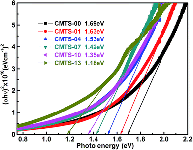 |
| | Fig. 7 Plot of (αhν)2 vs. hν for CMTS-00, CMTS-01, CMTS-04, CMTS-07, CMTS-10, and CMTS-13. | |
3.6 Device characterization
A photovoltaic device with a CMTS-10 absorber layer has been fabricated with the AZO/i-ZnO/CdS/CMTS/Mo/glass structural configuration. Cell-1, 2 and 3 in Fig. 8 are made with a CMTS-10 layer. J–V characteristics for the cell devices under simulated AM1.5 illumination are shown in Fig. 8, and all of the device parameters are listed in the inset of Fig. 8. Cell-3 gives a better power conversion efficiency (PCEs) of 0.49% with a short-circuit current density (Jsc) of 4.70 mA cm−2, an open-circuit potential (Voc) of 308.4 mV, a fill factor (FF) of 33.9%, a high series resistance (Rs) of 48.9 Ω cm2, and a low shunt resistance (Rsh) of 104.8 Ω cm2. Note that this is the first report on the synthesis of CMTS solar cells. Cell-1 and 2 are other devices in the same sample which are close to cell-3. They have PCEs of 0.42% and 0.43%, respectively, which indicates a relatively well controlled composition and quality distribution in the CMTS-10 absorber layer. In comparison to the photovoltaic parameters of the CMTS-10 device, those of the CZTS device are PCE = 6.6%, FF = 57.2%, Voc = 581.4 mV, Jsc = 19.9 mA cm−2, Rs = 5.3 Ω cm2 and Rsh = 282.8 Ω cm2.20 The PCEs in our device are predominantly limited by low Voc (308.4 mV), Jsc (4.70 mA cm−2), and FF (33.9%). The low Rsh can lead significantly to a low Voc, and the high Rs may result in a low FF value as well as a low Jsc.28 Generally, the high Rs might be attributed to the deterioration of charge transfer and the recombination of charge carriers at the CdS/CMTS interface, and the low Rsh can be ascribed to the small-grained CMTS layer.20 Therefore, further optimization of the annealing conditions and interface treatment are important for fabricating a homogenous CMTS absorber layer composed of large grain size and a pure phase in order to improve the device performance.
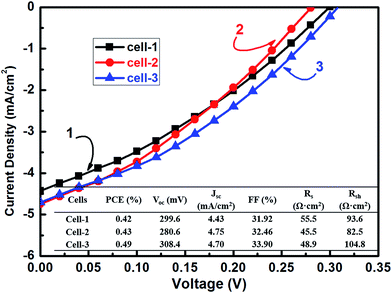 |
| | Fig. 8 Current–voltage (J–V) characteristics of the solar cell devices fabricated with CMTS-10, measured under AM1.5 simulated illumination. | |
4. Conclusions
A simple and non-toxic spin-coating method is introduced to prepare CMTS thin films. The effect of annealing time on the grown film was optimized. Specifically, annealing for a short time (<10 min) left the synthesis incomplete, yielding films where secondary phases coexist with CMTS. A longer annealing time (10 min) yields film with an upgraded degree of crystallinity, large grains and low dislocation density. Further increasing the annealing time to 13 min leads to the decomposition of CMTS into MnS, SnS and Cu2S phases. The surface morphology shows that increasing the annealing time generally leads to improved film morphology in the form of well-defined and densely packed CMTS grains. However, as the annealing time is further increased to 13 min, the overgrowth of grains on the film is observed resulting in a rough surface. The Cu content generally increases with the increase of annealing time with the Cu/(Mn + Sn) ratio increasing from 0.91 to 2.21. Analysis of transmission spectra for the post-annealed CMTS thin films shows that the band gap energy shifts toward lower energies gradually with increasing the annealing time from 1.63 to 1.18 eV; in particular, the as-prepared precursor film exhibits the largest band gap of 1.69 eV. The decrease of Eg values with increasing annealing time can be attributed to the combined effects of the improvement of the crystalline quality and the Cu/(Mn + Sn) ratio in the CMTS thin films. Most importantly, a CMTS solar cell (PEC = 0.49%, Jsc = 4.70 mA cm−2, Voc = 308.4 mV, and FF = 33.9%) with the common structure has been fabricated for the first time. This result offers the possibility for the application of a CMTS absorber layer in low-cost solar cells by further optimization of the preparation process.
Acknowledgements
This work was supported by the National Natural Science Foundation of China (61474045), and the State Key Basic Research Program of China (2013CB922300).
References
- P. Jackson, D. Hariskos, R. Wuerz, O. Kiowski, A. Bauer, T. M. Friedlmeier and M. Powalla, Phys. Status Solidi RRL, 2015, 9, 28–31 CrossRef CAS PubMed.
- K. Ito and T. Nakazawa, Jpn. J. Appl. Phys., Part 1, 1988, 27, 2094–2097 CrossRef CAS.
- M. Quintero, E. Moreno, S. Alvarez, J. Marquina, C. Rincón, E. Qunitero, P. Grima, J. A. Heano and M. A. Macías, Rev. LatinAm. Metal. Mat, 2014, 34, 28–38 Search PubMed.
- L. Chen, H. Deng, J. Tao, W. Zhou, L. Sun, F. Yue, P. Yang and J. Chu, J. Alloys Compd., 2015, 640, 23–28 CrossRef CAS PubMed.
- X. Liang, P. Guo, G. Wang, R. Deng, D. Pan and X. Wei, RSC Adv., 2012, 2, 5044–5046 RSC.
- C. Xu, H. Zhang, J. Parry, S. Perera, G. Long and H. Zeng, Sol. Energy Mater. Sol. Cells, 2013, 117, 357–362 CrossRef CAS PubMed.
- J. J. Scragg, T. Ericson, X. Fontané, V. Izquierdo-Roca, A. Pérez-Rod ríguez, T. Kubart, M. Edoff and C. Platzer-Björkman, Prog. Photovolt. Res. Appl., 2014, 22, 10–17 CrossRef CAS PubMed.
- L. Yin, G. Cheng, Y. Feng, Z. Li, C. Yang and X. Xiao, RSC Adv., 2015, 5, 40369–40374 RSC.
- S. C. Riha, B. A. Parkinson and A. L. Prieto, J. Am. Chem. Soc., 2009, 131, 12054–12055 CrossRef CAS PubMed.
- Y. Cui, R. Deng, G. Wang and D. Pan, J. Mater. Chem., 2012, 22, 23136–23139 RSC.
- T. K. Todorov, J. Tang, S. Bag, O. Gunawan, T. Gokmen, Y. Zhu and D. B. Mitzi, Adv. Energy Mater., 2013, 3, 34–38 CrossRef CAS PubMed.
- W. Wang, M. T. Winkler, O. Gunawan, T. Gokmen, T. K. Todorov, Y. Zhu and D. B. Mitzi, Adv. Energy Mater., 2014, 4, 1301465 Search PubMed.
- Z. Su, K. Sun, Z. Han, H. Cui, F. Liu, Y. Lai, J. Li, X. Hao, Y. Liu and M. A. Green, J. Mater. Chem. A, 2014, 2, 500–509 CAS.
- Y. Sun, Y. Zhang, H. Wang, M. Xie, K. Zong, H. Zheng, Y. Shu, J. Liu, H. Yan, M. Zhu and W. Lau, J. Mater. Chem. A, 2013, 1, 6880–6887 CAS.
- K. Maeda, K. Tanaka, Y. Fukui and H. Uchiki, Sol. Energy Mater. Sol. Cells, 2011, 95, 2855–2860 CrossRef CAS PubMed.
- V. Tunuguntla, W. Chen, P. Shih, I. Shown, Y. Lin, J. Hwang, C. Lee, L. Chen and K. Chen, J. Mater. Chem. A, 2013, 1–3 Search PubMed.
- J. Chen, Q. Chen, Y. Ni, Y. Yamaguchi, T. Wang, Z. Jia, X. Dou and S. Zhuang, J. Sol-Gel Sci. Technol., 2015, 75, 25–30 CrossRef CAS.
- K. Tanaka, Y. Fukui, N. Moritake and H. Uchiki, Sol. Energy Mater. Sol. Cells, 2011, 95, 838–842 CrossRef CAS PubMed.
- S. G. Kwon and T. Hyeon, Acc. Chem. Res., 2008, 41, 1696–1709 CrossRef CAS PubMed.
- J. Tao, K. Zhang, C. Zhang, L. Chen, H. Cao, J. Liu, J. Jiang, L. Sun, P. Yang and J. Chu, Chem. Commun., 2015, 51, 10337–10340 RSC.
- S. Wang, Q. Y. Gao and J. C. Wang, J. Phys. Chem. B, 2005, 109, 17281–17289 CrossRef CAS PubMed.
- A. Begum, A. Hussain and A. Rahman, Beilstein J. Nanotechnol., 2012, 3, 438–443 CrossRef PubMed.
- L. Chen, H. Deng, J. Cui, J. Tao, W. Zhou, H. Cao, L. Sun, P. Yang and J. Chu, J. Alloys Compd., 2015, 627, 388–392 CrossRef CAS PubMed.
- T. Fries and Y. Shapira, Phys. Rev. B: Condens. Matter Mater. Phys., 1997, 56, 5424–5431 CrossRef CAS.
- M. Himmrich and H. Haeuseler, Spectrochim. Acta, Part A, 1991, 47, 933–942 CrossRef.
- A. Anastassiadou, E. Liarokapis and E. Anastassakis, Phys. Scr., 1988, 38, 444–447 CrossRef CAS PubMed.
- J. He, L. Sun, Y. Chen, J. Jiang, P. Yang and J. Chu, RSC Adv., 2014, 4, 43080–43086 RSC.
- J. Tao, J. Liu, J. He, K. Zhang, J. Jiang, L. Sun, P. Yang and J. Chu, RSC Adv., 2014, 4, 23977–23984 RSC.
- D. Fan, R. Zhang, Y. Zhu, H. Peng and J. Zhang, J. Alloys Compd., 2014, 583, 566–573 CrossRef CAS PubMed.
- L. Sun, J. He, H. Kong, F. Yue, P. Yang and J. Chu, Sol. Energy Mater. Sol. Cells, 2011, 95, 2907–2913 CrossRef CAS PubMed.
- N. Moritake, Y. Fukui, M. Oonuki, K. Tanaka and H. Uchiki, Phys. Status Solidi C, 2009, 6, 1233–1236 CrossRef CAS PubMed.
- D. B. Khadka and J. Kim, J. Phys. Chem. C, 2014, 118, 14227–14237 CAS.
- S. Chen, A. Walsh, Y. Luo, J. Yang, X. G. Gong and S. H. Wei, Phys. Rev. B: Condens. Matter Mater. Phys., 2010, 82, 195203 CrossRef.
|
| This journal is © The Royal Society of Chemistry 2015 |
Click here to see how this site uses Cookies. View our privacy policy here.