Electronic transport properties of in-plane heterostructures constructed by MoS2 and WS2 nanoribbons

Yi Zhoua, Jichen Dongb and Hui Li*a
aKey Laboratory for Liquid-Solid Structural Evolution and Processing of Materials, Ministry of Education, Shandong University, Jinan 250061, People's Republic of China. E-mail: lihuilmy@hotmail.com
bDepartment of Mechanical and Biomedical Engineering, City University of Hong Kong, 83 Tat Chee Avenue, Hong Kong

Received 22nd July 2015 , Accepted 27th July 2015

First published on 27th July 2015


Abstract

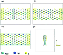
A new and simple kind of in-plane heterostructure is constructed by MoS2 nanoribbons (MoS2NRs) and WS2 nanoribbons (WS2NRs) arranged both perpendicularly and in parallel. The electronic transport properties of two-probe devices with these heterostructures are investigated by first-principle density functional theory and non-equilibrium Green function. The results indicate that for all these heterostructures, with the number of WS2NR unit cell increasing, the bandgap decreases slightly and the negative differential resistance (NDR) effect can be tuned. Especially for the case with W atoms doping on the edge, it not only displays a notable NDR effect but also has a high current peak under low bias, which indicates that it shows a better performance applied as a logic transistor. This study may provide a new path for the creation of the novel nanoelectronic devices with good performance.


I. Introduction

Following the discovery of graphene, considerable research interest has been focused on graphene-based nanoscale electronics and photonic devices as a result of the unique electronic characteristics and peculiar structure, such as the zero band gap semiconducting property and its massless charge carriers.1–7 Graphene field effect transistors (FETs) are most widely studied because FETs occupy the fundamental position on the integrated circuits. Many researchers have reported that graphene displays an exceptionally high carrier mobility, enabling fast-speed FETs to be fabricated.8–12 However, pristine graphene does not possess a band gap, a property that is critical for applications in logic transistors to attain a large on/off ratio.13–15 Therefore, it becomes an urgent issue that opening a sizable band gap for graphene must be solved by theoretical and experimental studies. Considerable methods have been used to tackle this issue, such as chemical decorations,16–19 applying a high electric field to bilayer graphene20–23 and cutting graphene into GNRs,24–26 but these methods add complexity and diminish mobility. To overcome this problem, it would be a better choice for seeking other semiconducting graphene-like materials.

More recently, 2D transition metal dichalcogenides (TMDs), which are composed of atomic layers coupled by van der Waals forces, have gained considerable interest because of the large variety of electronic phases that they can exhibit, namely, metallic, semiconductor, superconductor, and charge density wave.27–34 Unlike graphene, single-layer MoS2, a member of TMD family, is a semiconductor with a large bandgap,30 and hence monolayer MoS2 has been regarded as a promising candidate for field effect transistor (FET).35,36 MoS2 has a crystal structure consisting of weakly-coupled sandwich layers S–Mo–S, where a Mo-atom layer is enclosed within two S layers with hexagonal structure, and these layers are held together by van der Waals interactions.37 Owing to such a structure, single layer of MoS2 can be probably fabricated repeatedly one by one from bulk materials by micromechanical cleavage38 or exfoliation.39 Recently, MoS2 nanoribbons and other TMD materials with a width down to several nanometers have been synthesized.40–43 Importantly, among these TMDs, WS2 is expected to have similar properties with MoS2,44–47 and the first experimental demonstrations of monolayer WS2 have just been reported.48 Armchair MoS2 and WS2 nanoribbons have the same crystal structure and share the very similar lattice constants. The electronic properties of 2D heterostructures consisting of WS2 and MoS2 monolayer, which are stacked in vertical, have been studied.49–54 More recently, Gong et al.55 experimentally fabricated in-plane heterostructures of WS2/MoS2 with seamless and atomically sharp interface. However, little has been done to theoretically study the electronic properties of such in-plane heterostructures composed of MoS2NRs and WS2NRs.

In this work, we propose two kinds of armchair MoS2NRs and WS2NRs heterostructures arranged both in perpendicular and in parallel, that is, with the interfaces along the zigzag and armchair directions respectively. Systematic first-principles calculations are performed to study the electronic transport properties of two-probe devices with these heterostructures.

II. Models and methods

Fig. 1 shows the devices consisting of an armchair MoS2NRs/WS2NRs heterostructure. The devices are placed along the z direction, and the x axis is perpendicular to its surface. The two-probe device is composed of two parts, i.e., the scattering region and the electrodes, where the number of atoms are 179, the central region is six unit cells, electrode region is one unit cell. The yellow marked boxes denotes the supercell of the source and drain electrodes, between which is located the scattering region made of a hybrid MoS2NRs/WS2NRs structure. These devices are described by M(na) and M(nz), where n denotes the number of WS2NR unit cell in the scattering region, and a(z) indicates the armchair or zigzag shaped ribbon.
image file: c5ra14507d-f1.tif
Fig. 1 Schematics of MoS2NR/WS2NR two-probe devices. The yellow box denote the source and drain electrodes and unit cell of WS2NR are marked by dashed box. The whole device is situated in a supercell represented by solid rectangle. (a) Structure of M(1a) two-probe device. (b) Structure of M(1z) two-probe device. (c) Structure of M(edge) two-probe device. (d) Side view of the crystal structures.

All the calculations of these heterostructures are performed by the non-equilibrium Green function together with the first-principles density functional theory (DFT) supplied in the AtomistixToolKit software package.56,57 Double-zeta single polarized basis sets are adopted for the local atomic numerical orbitals, and norm-conserving pseudo-potentials are employed. Perdew–Burke–Ernzerhof (PBE) exchange-correlation function under the spin-unpolarized generalized gradient approximation (GGA) is implemented. Periodic boundary conditions are employed to calculate the electronic structures. The mesh cutoff for the electrostatic potentials is set to 75 Ha. A 1 × 1 × 100 Monkhorst sampling is utilized in the Brillouin zone integration. The electron temperature in the Fermi function is 300 K. To avoid interactions between periodic images, all heterostructures are modeled within a supercell with at least 15 Å vacuum layer thickness between neighboring cells. The energy convergence criterion is set to 10−5 eV. Before calculating the electronic properties, these devices and crystal structures are optimized until the forces acting on each atom are less than 0.05 and 0.01 eV Å−1, respectively. The device current Id is manifested by the Landauer–Büttiker equation:

image file: c5ra14507d-t1.tif
where f1,2(E) are the Fermi functions of source and drain electrodes, e is the electron charge, and h is Planck's constant, T(E,V) is the quantum mechanical transmission probability of electrons, and it can be given as:
T(E,V) = tr[ΓL(E,V)GR(E,V)ΓR(E,V)GA(E,V)]
where GR,A are the retarded/advanced Green functions of the conductor part and ΓR,L are the coupling functions to the left/right electrodes.

III. Results and discussion

In Gong et al.55 work, in-plane heterostructure of WS2/MoS2 with zigzag direction interface could be easily identified. Based on this heterostructure with the interfaces along the zigzag directions, we first construct M(na), where MoS2NRs and WS2NRs are arranged in perpendicular and investigate the effect of WS2NR length on the electron transport properties of these heterostructures. Fig. 2 shows IdVd characteristics of M(na) with lengths n ranging from 1 to 3. It is clear that in all three cases there is no current until 0.6 V bias, which exhibits a semiconducting property, and increasing the bias further they all exhibit NDR, with dips in the current occurring between 0.9 to 1.0 V bias. With the increase of the WS2NR length, not only the current increases more quickly, but PVR (Peak to Valley Ratio) also increases, namely, 3.01, 4.931 and 5.441, respectively, along with the same NDR window, that is 0.1 V, which indicates that it shows a relatively better performance in the application of logic transistor when contacting more unit cells of WS2NRs.
image file: c5ra14507d-f2.tif
Fig. 2 IdVd curves of M(na) with WS2NR length n ranging from 1 to 3.

We now investigate the physical origin of the NDR, the transmission spectrum is shown in Fig. 3(a) for M(3a) at several typical bias voltages and other points are presented in ESI Fig. 1. Under a small bias of 0.6 V, a little transmission peak moves into the bias window, resulting in an initial increase in current. As the bias increases further, the peak broadens and the current increases, reaching its maximum when the bias is 0.9 V. When the bias is larger than 0.9 V, the peak height decreases dramatically, and this decrease dominates positive contributions to the current rather than additional two small peaks moving into the bias window at 1.0 V bias, leading to the NDR. The peaks in the expanding bias window are enhanced by continuous increasing applied drain voltage to 1.4 V, giving rise to a steady increase in current. In Fig. 3(b) and (c), to illustrate the difference of these three curves, transmission spectrum is calculated at 0.9 and 1.0 V, respectively. When the bias is 0.9 V, the single peak height increases slowly with the increase of the WS2NR length, leading to a small increase in current peak. At the bias of 1.0 V, when n ranges from 1 to 3, two of three peaks height in the bias window decrease, which play an important role in decrease of current valley, although another small peak displays an opposite trend. In Fig. 3(b), as unit cell of WS2NR ranges from 1 to 2, the reduction extent of peaks denoted by b and c is more obvious than that from 2 to 3, resulting in a higher current valley for M(1a) heterostructure.


image file: c5ra14507d-f3.tif
Fig. 3 Transmission spectrum (a) for M(3a) at several typical bias voltages. Dotted line represent chemical potentials of the source and drain electrodes and for M(na) with WS2NR length n ranging from 1 to 3 (b) at the bias of 0.9 V and (c) at the bias of 1.0 V.

For a deep insight into the electronic transport properties, equilibrium density of states (DOS) of these devices and their corresponding band structure of crystal structures are calculated and shown in Fig. 4. Features of other M(na) are presented in ESI Fig. 2 because they are similar to each other except for some detailed distinctions. In Fig. 4(a), the curve of DOS indicates that zero electron states occur at Ef because of the semiconductor characteristics of armchair MoS2 and WS2 nanoribbons, not resulting in electron transmission at Ef, which corresponding to IdVd characteristics that there is no current until 0.6 V bias. Moreover the transmission peaks are consistent with that of DOS around Ef. Importantly, the total density of states (TDOS) and the projected density of states on the edge (PDOS-edge) almost coincide with each other in the energy range from −0.4 to 1.2 eV, which implies that electron states near Ef mainly originate from the edge. To describe this phenomenon clearly, local density states (LDOS) at −0.18 eV is calculated and shown in Fig. 4(b), it is clear that LDOS is mainly on the W and Mo atoms of the two edges, and becomes bigger and bigger with the increase of the WS2NR length (shown in ESI Fig. 2). The above discussion means that electrons transport through the central region mainly from the transition metal atoms of the edge due to the effect of dangling bonds. The band structure further demonstrates that armchair MoS2NRs can remain semiconducting by contacting WS2NRs and there is a direct band gap with its lowest unoccupied conductance band minimum (LUCBM) and highest occupied valence band maximum (HOVBM) both at Γ point in the Brillouin zone in Fig. 4(c) and the optical characteristics of MoS2 are retained when contacted WS2, meaning these heterostructures can be also applied in optoelectronic devices to investigate the changes of LUCBM and HOVBM clearly, the information is extracted and given in Fig. 4(d). It can be seen, when n increasing from 1 to 3, LUCBM decreases and HOVBM increases, giving rise to a decrease in bandgap (Eg). Although the change is not obvious, when the bias is applied, it leads to the quick increase of the current, and the higher current peak. The variation of the bandgap is consistent with Gong et al.55 work that the PL peak position shifted continuously across the interface.


image file: c5ra14507d-f4.tif
Fig. 4 (a) Equilibrium transmission spectrum and total and projected DOS of M(3a). (b) LDOS at Ef −0.18 eV of M(3a) with an isovalue of 0.1. (c) Band structures of M(3a). (d) HOVBM and LUCBM and bandgap for M(na) with WS2NR length n ranging from 1 to 3.

In addition, as Gong et al.55 work mentioned, besides the preferred zigzag interface, in-plane heterostructures of WS2/MoS2 along the armchair direction were also occasionally observed in their sample. Based on this structure with the interfaces along the armchair directions, electronic properties of such structure consisting of MoS2NRs and WS2NRs arranged in parallel with the increase of WS2NR length are also studied. In Fig. 5, IdVd characteristics of M(nz), where n ranges from 1 to 4, are shown. Apparently, the curves all display the NDR effect under a drain bias sweep from 0.9 to 1.0 V. Besides, another NDR effect is observed from 1.2 to 1.4 V for M(4z) two-probe device, and the PVR is 1.001. With WS2NR width increasing from 1 to 4, the NDR window remains the 0.1 V, but PVR decreases, that is, 3.3037, 2.7585, 1.6063, 1.003, respectively. Although the NDR effect weakens when contacting more unit cells of WS2NR, the current is enhanced obviously. Especially for M(4z), the current increase more quickly than the others, while the NDR is very low, indicating that it would be not the good candidate in the application of logic transistor.


image file: c5ra14507d-f5.tif
Fig. 5 IdVd curves of M(nz) with WS2NR length n ranging from 1 to 4.

To understand the observed NDR effect, it is useful to analyze the evolution of the transmission spectrum as the bias potential is ramped up for M(1z) in ESI Fig. 3 and some typical biases are shown in Fig. 6(a). When a small bias of 0.6 V applied, transmission peak begins to appear in the bias window, giving rise to an original current increase. Before 0.9 V bias, the applied bias simultaneously enhances the only one peak height, increasing the weight of the transmission spectrum in the bias window and current. The overall reduction in peak height outweighs increase from an additional peak moving into the expanding bias window, leading to a net drop in current and the appearance of NDR at 1.0 V. With a further increase of the bias to 1.4 V, the peaks broaden together with more peaks moving into the extending bias window, which results in a steady current increase. In contrast to M(1z), transmission spectrum at different bias potential from 0.6 to 1.4 V is shown in ESI Fig. 4 for M(4z) and several typical biases are presented in Fig. 6(b). It is more obvious that the initial peak occurs in the bias window and the height appearance with increasing bias. After the bias of 0.9 V, the weights of the transmission spectrum in the bias window decrease slightly both at 1.0 V and 1.4 V bias, which results in twice NDR effect with small PVR. To clearly identify the distinction among the four cases, transmission spectra of 0.9 and 1.0 V bias are calculated, and shown in Fig. 6(c) and (d). As WS2NR width increases from 1 to 4, the transmission peaks in both biases broaden, leading to an increase in either current peak or valley, however for bias of 0.9 V the extent is less obvious than 1.0 V bias, and results in a decrease in PVR.


image file: c5ra14507d-f6.tif
Fig. 6 Transmission spectrum for (a) M(1z) and (b) M(4z) at several typical bias voltages. Dotted line represent chemical potentials of the source and drain electrodes. Transmission spectrum for M(nz) with WS2NR length n ranging from 1 to 4 (c) at the bias of 0.9 V and (d) at the bias of 1.0 V.

To identify the nature states of the electronic transport properties, equilibrium TDOS and PDOS of M(1z) two-probe devices are calculated, just as shown in Fig. 7(a). Due to the semiconducting property of armchair MoS2 nanoribbons, no electron and its transmission states are observed at Ef, which corresponding to the transmission spectrum that transmission peak begins to appear in the bias window when a small bias of 0.6 V applied, the PDOS-edge is almost consistent with TDOS around Fermi energy, which leads to the transmission spectrum, indicating that electron transmission states mainly localize on the edge. To clearly see this phenomenon, local density states (LDOS) at −0.18 eV is calculated and given in Fig. 7(b), it shows that the electron states at −0.18 eV is mainly on the Mo atoms of the two edges. As discussed above, electrons from the transition metal atoms of the edge can transport through the central region more easily because the Mo atoms of the edge have higher energy with unfilled d orbit. Moreover, band structure of the crystal is analyzed in Fig. 7(c). We can see that for all the four heterostructures, both LUCBM and HOVBM localize at Γ point in the Brillouin zone (shown in ESI Fig. 5), which exhibits direct band gap semiconducting characteristics. The optical characteristics of MoS2 do not change after contacting WS2, which means that these heterostructures can be also applied in optoelectronic devices. In Fig. 7(d), we can see that as LUCBM decreases and HOVBM increases, there is a slight decrease in bandgap with the increase of the WS2NR width, therefore the current increases more quickly with a higher current peak despite a small decline when bias is applied. Gong et al.55 found that the PL peak position shifted continuously across the interface that corresponds to the change of the bandgap of our work.


image file: c5ra14507d-f7.tif
Fig. 7 (a) Equilibrium transmission spectrum and total and projected DOS of M(1z). (b) LDOS at Ef −0.18 eV of M(1z) with an isovalue of 0.1. (c) Band structures of M(1z). (d) HOVBM and LUCBM and bandgap for M(nz) with WS2NR length n ranging from 1 to 4.

Lastly, we study the another heterostructure denoted by M(edge) that Gong et al.55 did not discuss, in which the Mo atoms on the edges are replaced by W atoms. Due to the same amount of W doping, M(1z) makes a comparison with this heterostructure to investigate whether edge states influence electronic transport properties. IdVd characteristics of M(edge) is illustrated in Fig. 8. Compared with M(1z), M(edge) also exhibits NDR effect with a wider NDR window between 0.9 V to 1.2 V rather than 1.0 V. When the bias is larger than 0.6 V with an initial current, the curve of the latter increases more rapidly until reaching its maximum where the current is almost similar to the case of M(4z). Moreover, the current valley is the lowest among the above four heterostructures, resulting in a largest PVR, which is 18.4462. Although M(edge) shares the same amount of W doping with M(1z), the performance of M(edge) is enhanced heavily with a wider NDR window, six times higher PVR which means a better NDR effect and a higher current peak. Because the energy of W atoms on the edge is higher than that on the inner, the current is increased quickly. Compared to M(4z) with the highest current peak among this type of heterostructures, M(edge) is almost close to it in the current peak but shows a superior NDR effect. As discussed above, M(edge) not only displays a notable NDR effect but also has a high current peak under low bias, which would be the best candidate in the application of logic transistor.


image file: c5ra14507d-f8.tif
Fig. 8 IdVd curves of M(edge) and M(nz) with WS2NR length n ranging from 1 to 4.

To understand the physical origin of the NDR, transmission spectrum is calculated as the bias voltages ranging from 0.6 to 1.4 V, and shown in ESI Fig. 6. Fig. 9(a) presents several typical bias voltages. As 0.6 V bias is applied, transmission peak starts to move into the bias window, leading to an initial current. Before the bias of 1.2 V, the single peak firstly broadens up to its maximum at 0.9 V bias, and then reduces dramatically into two small peaks, which results in the NDR effect. To clearly illustrate the difference between the two cases, Fig. 9(b–d) shows transmission spectrum at the bias of 0.9, 1.0 and 1.2 V, respectively. For M(edge), when the bias is 0.9 V and 1.0 V, the contribution of the transmission peaks in the bias window is larger than its counterpart, giving rise to a higher current. Conversely, at 1.2 V bias, the two peaks height are both lower than the case of M(1z), leading to a small current.


image file: c5ra14507d-f9.tif
Fig. 9 (a) Transmission spectrum for M(edge) at various bias voltages. Dotted line represent chemical potentials of the source and drain electrodes. Transmission spectrum for M(1z) and M(edge) (b) at the bias of 0.9 V, (c) at the bias of 1.0 V and (d) at the bias of 1.2 V.

IV. Conclusions

In this study, we put forward two kinds of in-plane heterostructures composed of MoS2NRs and WS2NRs arranged in perpendicular and in parallel respectively which can be fabricated in practice, and investigate the electronic transport properties of these heterostructures using non-equilibrium Green function and the first-principles DFT calculations. It is found that for all the heterostructures, they exhibit direct band gap semiconducting characteristics at Γ point, which means that these heterostructures can be applied in optoelectronic devices and bandgap decreases slightly as the number of WS2NR unit cell increases, resulting in the rapid increase of the current and the higher current peak. In addition, for M(na), the NDR effect is enhanced little with the number of WS2NR unit cell increasing, while for M(nz), it exhibits an opposite trend but the current increases more quickly with a higher current peak, which indicates that the heterostructures arranged in perpendicular have a better application than those in parallel in logic transistor. Especially for M(edge) with W atoms doping on the edge, it shows the best performance in the application of logic transistor, because it not only displays a notable NDR effect but also has a high current peak under low bias. With these unique properties, it is expected that MoS2NR/WS2NR heterostructures promote the applications in the next generation nanoelectronic devices.

Acknowledgements

The authors would like to acknowledge the support from the National Natural Science Foundation of China (Grant No. 51271100). This work is also supported by the National Basic Research Program of China (Grant No. 2012CB825702). This work is also supported by the Special Funding in the Project of the Taishan Scholar Construction Engineering.

References

  1. K. A. Ritter and J. W. Lyding, Nat. Mater., 2009, 8, 235–242 CrossRef CAS PubMed.
  2. L. Shen, M. G. Zeng, S. W. Yang, C. Zhang, X. F. Wang and Y. P. Feng, J. Am. Chem. Soc., 2010, 132, 11481–11486 CrossRef CAS PubMed.
  3. J. M. Mativetsky, A. Liscio, E. Treossi, E. Orgiu, A. Zanelli, P. Samorì and V. Palermo, J. Am. Chem. Soc., 2011, 133, 14320–14326 CrossRef CAS PubMed.
  4. R. M. Westervelt, Science, 2008, 320, 324–325 CrossRef CAS PubMed.
  5. K. S. Novoselov, A. K. Geim, S. V. Morozov, D. Jiang, Y. Zhang, S. V. Dubonos, I. V. Grigorieva and A. A. A. Firsov, Science, 2004, 306, 666–669 CrossRef CAS PubMed.
  6. J.-H. Chen, C. Jang, S. Xiao, M. Ishigami and M. S. Fuhrer, Nat. Nanotechnol., 2008, 3, 206–209 CrossRef CAS PubMed.
  7. F. Chen, J. Xia, D. K. Ferry and N. Tao, Nano Lett., 2009, 9, 2571–2574 CrossRef CAS PubMed.
  8. Y. M. Lin, C. Dimitrakopoulos, K. A. Jenkins, D. B. Farmer, H. Y. Chiu, A. Grill and P. Avouris, Science, 2010, 327, 662 CrossRef CAS PubMed.
  9. M. J. Hollander, M. LaBella, Z. R. Hughes, M. Zhu, K. A. Trumbull, R. Cavalero, D. W. Snyder, X. J. Wang, E. Hwang, S. Datta and J. A. Robinson, Nano Lett., 2011, 11, 3601–3607 CrossRef CAS PubMed.
  10. L. Liao, J. W. Bai, Y. Q. Qu, Y. C. Lin, Y. J. Li, Y. Huang and X. F. Duan, Proc. Natl. Acad. Sci. U. S. A., 2001, 107, 6711–6715 CrossRef PubMed.
  11. D. C. Elias, R. V. Gorbachev, A. S. Mayorov, A. A. Zhukov, P. Blake, L. A. Ponomarenko, I. V. Grigorieva, K. S. Novoselov, F. Guinea and A. K. Geim, Nat. Phys., 2011, 7, 701–704 CrossRef CAS PubMed.
  12. A. S. Mayorov, R. V. Gorbachev, S. V. Morozov, L. Britnell, R. Jalil, L. A. Ponomarenko, P. Blake, K. S. Novoselov, K. Watanabe, T. Taniguchi and A. K. Gein, Nano Lett., 2011, 11, 2396–2399 CrossRef CAS PubMed.
  13. A. H. Castro Neto, F. Guinea, N. M. R. Peres, K. S. Novoselov and A. K. Geim, Rev. Mod. Phys., 2009, 81, 109–162 CrossRef CAS.
  14. L. Liao, J. W. Bai, Y. Q. Qu, Y. C. Lin, Y. J. Li, Y. Huang and X. F. Duan, Proc. Natl. Acad. Sci. U. S. A., 2010, 107, 6711–6715 CrossRef CAS PubMed.
  15. X. Li, W. W. Cai, J. H. An, S. Y. Kim, J. Nah, D. X. Yang, R. Piner, A. Velamakanni, I. Jung, E. Tutuc, S. K. Banerjee, L. Colombo and R. S. Ruoff, Science, 2009, 324, 1312–1314 CrossRef CAS PubMed.
  16. R. Balog, B. Jørgensen, L. Nilsson, M. Andersen, E. Rienks, M. Bianchi, M. Fanetti, E. Lægsgaard, A. Baraldi, S. Lizzit, Z. Sljivancanin, F. Besenbacher, B. Hammer, T. G. Pedersen, P. Hofmann and L. Hornekær, Nat. Mater., 2010, 9, 315–319 CrossRef CAS PubMed.
  17. L. Gan, J. Zhou, F. Ke, H. Gu, D. N. Li, Z. H. Hu, Q. Sun and X. F. Guo, NPG Asia Mater., 2012, 4(11), e31 CrossRef PubMed.
  18. W. J. Zhang, C. T. Lin, K. K. Liu, T. Tite, C. Y. Su, C. H. Chang, Y. H. Lee, C. W. Chu, K. H. Wei, J. L. Kuo and L. J. Li, ACS Nano, 2011, 5, 7517–7524 CrossRef CAS PubMed.
  19. J. C. Dong and H. Li, J. Phys. Chem. C, 2012, 116, 17259–17267 CAS.
  20. Y. Zhang, T.-T. Tang, C. Girit, Z. Hao, M. C. Martin, A. Zettl, M. F. Crommie, Y. R. Shen and F. Wang, Nature, 2009, 459, 820–823 CrossRef CAS PubMed.
  21. E. V. Castro, K. S. Novoselov, S. V. Morozov, N. M. R. Peres, J. M. B. Lopes dos Santos, J. Nilsson, F. Guinea, A. K. Geim and A. H. Castro Neto, Phys. Rev. Lett., 2007, 99, 216802–216805 CrossRef.
  22. T. Ohta, A. Bostwick, T. Seyller, K. Horn and E. Rotenberg, Science, 2006, 313, 951–954 CrossRef CAS PubMed.
  23. Y. B. Zhang, T. T. Tang, C. Girit, Z. Hao, M. C. Martin, A. Zettl, M. F. Crommie, Y. R. Shen and F. Wang, Nature, 2009, 459, 820–823 CrossRef CAS PubMed.
  24. X. Li, X. Wang, L. Zhang, S. Lee and H. Dai, Science, 2008, 319, 1229–1232 CrossRef CAS PubMed.
  25. Y. W. Son, M. L. Cohen and S. G. Louie, Phys. Rev. Lett., 2006, 97, 216803–216806 CrossRef.
  26. J. Hicks, A. Tejeda, A. Taleb-Ibrahimi, M. S. Nevius, F. Wang, K. Shepperd, J. Palmer, F. Bertran, P. Le Fèvre, J. Kunc, W. A. de Heer, C. Berger and E. H. Conrad, Nat. Phys., 2013, 9, 49–54 CrossRef CAS PubMed.
  27. H. Zhang, X.-B. Li and L.-M. Liu, J. Appl. Phys., 2013, 114, 093710 CrossRef PubMed.
  28. M. Chhowalla, H. S. Shin, G. Eda, L.-J. Li, K. P. Loh and H. Zhang, Nat. Chem., 2013, 5, 263 CrossRef PubMed.
  29. H. Zhang, L.-M. Liu and W.-M. Lau, J. Mater. Chem. A, 2013, 1, 10821 CAS.
  30. J. A. Wilson and A. D. Yoffe, Adv. Phys., 1969, 18, 193–335 CrossRef CAS PubMed.
  31. R. Fivaz and E. Mooser, Phys. Rev., 1967, 163, 743–755 CrossRef CAS.
  32. B. Radisavljevic, A. Radenovic, J. Brivio, V. Giacometti and A. A. Kis, Nat. Nanotechnol., 2011, 6, 147–150 CrossRef CAS PubMed.
  33. J. T. Ye, Y. J. Zhang, R. Akashi, M. S. Bahramy, R. Arita and Y. Iwasa, Science, 2012, 338, 1193–1196 CrossRef CAS PubMed.
  34. R. L. Withers and J. A. Wilson, J. Phys. C: Solid State Phys., 1986, 19, 4809–4845 CrossRef CAS PubMed.
  35. H. Liu, A. T. Neal and P. D. Ye, ACS Nano, 2012, 6, 8563–8569 CrossRef CAS PubMed.
  36. B. Radisavljevic and A. A. Kis, Nat. Mater., 2013, 12, 815–820 CrossRef CAS PubMed.
  37. J. L. Verble, T. J. Wietling and P. R. Reed, Solid State Commun., 1972, 11, 941–944 CrossRef CAS.
  38. K. S. Novoselov, D. Jiang, F. Schedin, T. J. Booth, V. V. Khotkevich, S. V. Morozov and A. K. Geim, Proc. Natl. Acad. Sci. U. S. A., 2005, 102, 10451–10453 CrossRef CAS PubMed.
  39. J. N. Coleman, M. Lotya, A. O'Neill, S. D. Bergin, P. J. King, U. Khan, K. Young, A. Gaucher, S. De and R. J. Smith, Science, 2011, 331, 568–571 CrossRef CAS PubMed.
  40. Z. Wang, H. Li, Z. Liu, Z. Shi, J. Lu, K. Suenaga, S.-K. Joung, T. Okazaki, Z. Gu, J. Zhou, Z. Gao, G. Li, S. Sanvito, E. Wang and S. Iijima, J. Am. Chem. Soc., 2010, 132, 13840–13847 CrossRef CAS PubMed.
  41. X. Liu, T. Xu, X. Wu, Z. Zhang, J. Yu, H. Qiu, J.-H. Hong, C.-H. Jin, J.-X. Li, X.-R. Wang, L.-T. Sun and W. Guo, Nat. Commun., 2013, 4, 1776 CrossRef PubMed.
  42. Z. Liu, K. Suenaga, Z. Wang, Z. Shi, E. Okunishi and S. Iijima, Nat. Commun., 2013, 2, 213 CrossRef PubMed.
  43. C. Nethravathi, A. Anto Jeffery, M. Rajamathi, N. Kawamoto, R. Tenne, D. Golberg and Y. Bando, ACS Nano, 2013, 7, 7311–7317 CrossRef CAS PubMed.
  44. Z. Y. Zhu, Y. C. Cheng and U. Schwingenschlögl, Phys. Rev. B: Condens. Matter Mater. Phys., 2011, 84, 153402 CrossRef.
  45. H. Jiang, J. Phys. Chem. C, 2012, 116, 7664 CAS.
  46. A. Ramasubramaniam, Phys. Rev. B: Condens. Matter Mater. Phys., 2012, 86, 115409 CrossRef.
  47. W. Feng, Y. Yao, W. Zhu, J. Zhou, W. Yao and D. Xiao, Phys. Rev. B: Condens. Matter Mater. Phys., 2012, 86, 165108 CrossRef.
  48. H. R. Gutierrez, N. Perea-López, A. L. Elías, A. Berkdemir, B. Wang, R. Lv, F. López-Urías, V. H. Crespi and H. Terrones, Nano Lett., 2013, 13, 3447–3454 CrossRef CAS PubMed.
  49. C. Gong, H. Zhang, W. Wang, L. Colombo, R. M. Wallance and K. Cho, Appl. Phys. Lett., 2013, 103, 053513 CrossRef PubMed.
  50. H. Komsa and A. Krasheninnikov, Phys. Rev. B: Condens. Matter Mater. Phys., 2013, 88, 085318 CrossRef.
  51. J. Kang, S. Tongay, J. Zhou, J. Li and J. Wu, Appl. Phys. Lett., 2013, 102, 012111 CrossRef PubMed.
  52. H. Terrones, F. López-Urías and M. Terrones, Sci. Rep., 2013, 3, 1549 Search PubMed.
  53. W.-T. Hsu, Z.-A. Zhao, L.-J. Li, C.-H. Chen, M.-H. Chiu, P.-S. Chang, Y.-C. Chou and W.-H. Chang, ACS Nano, 2014, 8, 2951–2958 CrossRef CAS PubMed.
  54. H. Fang, C. Battaglia, C. Carraro, S. Nemsak, B. Ozdol, J. S. Kang, H. A. Bechtel, S. B. Desai, F. Kronast, A. A. Unal, G. Conti, C. Conlon, G. K. Palsson, M. C. Martin, A. M. Minor, C. S. Fadley, E. Yablonovitch, R. Maboudian and A. Javey, Proc. Natl. Acad. Sci. U. S. A., 2014, 111, 6198–6202 CrossRef CAS PubMed.
  55. Y. Gong, J. Lin, X. Wang, G. Shi, S. Lei, Z. Lin, X. Zou, G. Ye, R. Vajtai, B. I. Yakobson, H. Terrones, M. Terrones and P. M. Ajayan, Nat. Mater., 2014, 13, 1135–1142 CrossRef CAS PubMed.
  56. M. Brandbyge, J. L. Mozos, P. Ordejon, J. Taylor and K. Stokbro, Phys. Rev. B: Condens. Matter Mater. Phys., 2002, 65, 165401–165417 CrossRef.
  57. ATK, version 2010.8, QuantumWise, Copenhagen, Denmark, 2008, www.quantumwise.com Search PubMed.

Footnote

Electronic supplementary information (ESI) available. See DOI: 10.1039/c5ra14507d

This journal is © The Royal Society of Chemistry 2015