Evaluation of a metal free dye for efficient dye sensitized solar cells based on hydrothermally synthesized TiO2 nanoflowers

Chang Su Shim a, Sawanta S. Mali a, Ryota Aokie b, Masski Matsui b, K. Manseki c and Chang Kook Hong *a
aDepartment of Chemical Engineering, Chonnam National University, Gwangju, South Korea 500-757. E-mail: hongck@chonnam.ac.kr
bDepartment of Materials Science and Technology, Faulty of Engineering, Gifu University, Yanagido, Gifu, Japan 501-1193
cGraduate School of Engineering, Environmental and Renewable Energy System (ERES) Division, Gifu University, Yanagido, Gifu, Japan 501-1193

Received 21st July 2015 , Accepted 19th October 2015

First published on 19th October 2015


Abstract

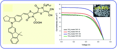
The main aim of the present investigation is to evaluate dye sensitized solar cells (DSSCs) properties of hydrothermally synthesized 3D TiO2 nanoflowers based on DN350 organic dye. The dye loading time has been optimized from the current–voltage (JV) characteristics in order to obtain high performance DSSCs. Further TiCl4 surface treatment was conducted for effective dye loading and fast electron transport for the improvement of DSSC performance. The dye loading and its performance evaluation has been optimized and analysed using JV performance, UV-vis spectroscopy and incident-photon-to-electron conversion efficiency (IPCE) etc. characterization techniques. The diffusion coefficient, diffusion length and electron life time have be evaluated using intensity-modulated photocurrent and photovoltage experiments (IMPS/IMVS). Our optimized results show that 30 min TiCl4 treated TNF samples exhibit current density (JSC) = 14.70 mA cm−2, open circuit voltage (VOC) = 0.650 V, Fill Factor (FF) = 0.62 and power conversion efficiency (PCE) = 5.92%.


1. Introduction

Dye-sensitized solar cells (DSSCs) have become one of the most promising alternatives in low-cost photovoltaic technology. Low-cost material, easy fabrication and relatively high conversion efficiency are the promising factors of DSSCs.1 Mesoporous TiO2 (mp-TiO2), a light absorber (dye), an iodine based redox electrolyte and catalytic Pt-FTO counter electrodes are key components of the DSSC architecture. The mp-TiO2, dye loading time and effective catalytic section boost the conversion efficiency. Usually, Ru-based dye requires 24 h dye loading time which is needed for the formation of a monolayer on the metal oxide. However, due to low dietetic constant and low conductivity of organic dyes, optimization of dye loading time strongly influences its performance. On the other hand, organic dyes have many more anchoring sites that facilitate easy adsorption onto the metal oxide surface. The small-sized particles suffer from grain boundaries and insufficient light scattering, thus resulting in low light-harvesting efficiency.2 Moreover, Frank et al. discussed limitations of electron diffusion coefficient and electron collection time in such nanoparticulate samples, which stem mainly from the prevailing hopping mechanism in them.3 On the other hand, the one dimensional (1D) TiO2 or ZnO nanostructures could provide slow recombination rate, fast electron transport and effective light scattering ability within the nanostructures. While, 3D nanostructures such as hierarchical microspheres4 nanoflowers5,6 functioning high specific surface area results in an effective dye adsorptive and light-scattering layer. The nanostructures of metal oxides and its composites will open new approaches toward efficient DSSCs. Muduli et al. synthesized TiO2-MWCNT nanocomposite and demonstrated 7.37% PCE using cis-bis(isothiocyanato)bis(2,2′-bipyridyl-4,4′-dicarboxylato)-ruthenium(II)bis-tetrabutylammonium (N-719) dye.7 On the other hand, Jiang et al. developed ZnO-nanoflower array with 1.9% PCE using cis-bis(isothiocyanato)bis(2,2′-bipyridyl-4,4′-dicarboxylato)-ruthenium(II)bis-tetrabutylammonium (N-719) dye. This efficiency has been obtained due to better dye loading and light harvesting of the ZnO-nanoflower structures.8 To tackle these problems, one dimensional (1-D) growth of nanostructured metal oxides is the effective solution, which can provide a direct path for the rapid collection of photogenerated electrons and reduce the charge recombination. Recently, hierarchical nano/microstructures like hierarchical SnO2 nanoflowers,9 hierarchical SnO2 octahedra10 are used as light-scattering layer with TiO2 and demonstrated 6.2% and 5.6% power conversion efficiency. Therefore such hierarchical nano/microstructures have attracted much attention in DSSCs owing to the improvement of effective light harvesting, fast transport pathway and effective dye loading. Taking into advantages of hydrothermal technique, we have developed surfactant free hydrothermal synthesis route for 1D as well as 3D TiO2 nanostructures with well-defined shape and size.5 Such 1D nanorods arrays with 3D dendrites are provide not only effective surface area but also helpful for effective light harvesting in DSSCs.

It is well known that, ruthenium based dyes are expensive and rare which hampers the cost-effectiveness of DSSCs technology. Therefore metal-free indoline/organic dyes open a unique opportunity towards cost-effective eco-friendly building photovoltaic (BIPV) technology. Recently we have studied variety of organic dyes including DN149, D205, DN319 etc. with mp-TiO2 and ZnO.11

To the author's best knowledge there is no single report available based on TiO2 nanoflowers DN350 organic dye. With this aspect of the limited resources of noble metal, metal-free organic dyes have been introduced for DSSCs.12–14 The indoline based organic dye D149 was introduced15 for DSSC with 6.1% conversion efficiency based on the TiO2. The indoline dye (D205) in which the ethyl group of D149 is substituted with octyl group has been reported to improve the open-circuit voltage (VOC) from the blocking of the charge recombination.14 The DN319 dye, in which the thiocarbonyl group of D205 in the terminal rhodanine moiety was converted into a dicyanovinylidene unit to achieve higher conversion efficiency than D205 based on the ZnO. Here more bathochromic absorption band plays an important role in fast transportation with good absorption of DN319 dye.16 The DN350 shows higher conversion efficiency due to bathochromic absorption band and prevention of aggregates formation.16 In DN350 dye, the 4-(2,2-diphenyvinyliden)phenylene moiety of DN319 is substituted with 2-(9,9-dimethylfluorenyl) group, has been reported to higher efficiency of 5.6% on the ZnO than DN319 due to prevention of aggregates formation of dye elevated by our group.17 The present study is focused on the evaluation of hydrothermally grown 3D TiO2 nanoflowers and organic dye DN350 for the DSSCs applications. Initially, hydrothermally grown 3D TiO2 nanoflowers were treated with TiCl4 and dye loading time has been optimized.

2. Experimental

2.1. Methods

Titanium(IV) butoxide (C16H36O4Ti) (Aldrich, 97%) (TBT) was dissolved in equal volume of concentrated HCl (37% Sigma Aldrich) and distilled water by magnetic stirring. The fluorine doped tin oxide coated glass (FTO) substrate was then immersed into the solution parallel to the Teflon wall. The sealed autoclave was then kept in a furnace for 3 h at 180 °C. More experimental details are available in our previous report.5,6 For the comparison we have used commercial TiO2 paste (P25, ENB Korea, TTP-20N, ENB-T12010501). The FTO (FTO, Pilkington TEC™ 7 Ω cm−2) glasses were washed with soap, water, ethanol and isopropanol each of 15 min using the ultrasonication. Commercial TiO2 (P25) paste was deposited on FTO glass substrate using doctor blade technique (device area 0.25 cm2), and then gradually heated at 550 °C for 10 min. The sintered mp-TiO2 films, as well as hydrothermally grown 3D TiO2 nanoflower samples, are showing ∼8.5 μm thickness. For TiCl4 treatment, the deposited TNF and TiO2 photoelectrodes were immersed in 0.04 M TiCl4 solution at 70 °C for 30 min. After treated samples are gradually heated 550 °C for 10 min. The sintered TNF and mp-TiO2 films are immersed in 0.5 mM DN350 dye solution (0.5 mM in a mixture of acetonitrile and tert-butylalchol (v/v, 1[thin space (1/6-em)]:[thin space (1/6-em)]1) with 0.5 mM chenodeoxycholic acid) at room temperature. The DN350 organic dye was synthesized as described in the literature.16 The Pt/FTO counter electrodes were prepared by commercial Pt-paste (Solaronix) as doctor blade technique. The iodide-based electrolyte (acetonitrile, valeronitrile (v/v, 85[thin space (1/6-em)]:[thin space (1/6-em)]15) with 0.1 M lithium iodide, 0.6 M butylmethylimidazolium iodide, 0.05 M I2, 0.05 M 4-tert-butylpyriine)14 was used as the redox electrolyte and injected into the interelectrode space from the counter electrode side through a pre-drilled hole. Dye adsorbed TiO2 samples are washed with ethanol and dried. For the measurement of dye loading amount, the dried electrodes were immersed in 20 mL dimethyl formamide (DMF, Daujung) solution at 50 °C in 24 h and the dye was totally desorbed in solvent from the electrode.

2.2. Characterizations

The surface morphology of the sample was recorded by a field emission scanning electron microscope (FESEM; S-4700, Hitachi). Transmission electron microscopy (TEM) micrographs, selected area electron diffraction (SAED) pattern and high-resolution transmission electron microscopy (HRTEM) images were obtained by TECNAI F20 Philips operated at 200 kV. The DSSC performances of cells were measured using a solar simulator at AM 1.5 G for 10 s, where the light intensity was adjusted with an NREL-calibrated Si solar cell with a KG-5 filter to 1 sun intensity (100 mW cm−2). The incident-photon-to-current conversion efficiency (IPCE) spectra were measured as a function of wavelength from 300 nm to 800 nm on the basis of a Spectral Products DK240 monochromator. The electron transport time and life time was measured by intensity-modulated photocurrent (IMPS) and photovoltage (IMVS) (Electronic-Chemical Analyzer; Iviumstat, HS technology) with varied the voltage from 0.550 to 1.000 V with amplitude from 0.00825 to 0.01500 Hz. The dye absorption and dye loading amount on the electrode was measured by UV-vis spectroscopy (Hitachi U-4000, F-4500) range and wavelength. The dye loading amount was measured from desorbed in 20 mL dimethylformamide (DMF, Daujung) solution absorption graph and calculated by a proportional expression from the reference of 0.5 M DN350 dye solution of UV absorption peak intensity at 567 nm.

3. Results and discussion

3.1. Morphological and structural characterization

Fig. 1(a) shows structural representation of an indoline DN350 dye. We have synthesized DN350 dye as per our previous report.17Fig. 1(b) shows typical micrograph of mesoporous TiO2 deposited and sintered on to FTO substrate. The FESEM image shows around 20 nm size mesoporous TiO2 nanoparticles are uniformly deposited throughout the surface. This commercial TiO2 paste (P25) TTP-20N, ENB-T12010501 was used as a reference electrode. Fig. 1(c) shows surface morphology of TiO2 nanoflowers (TNF) was synthesized by hydrothermal method. The SEM image shows nanoflowers like morphology having bunch of aligned nanorods. The diameter of nanorod is around 150 to 180 nm and total size of nanoflowers is around 2 μm as shown in Fig. 1(d). Fig. 1(e) shows spotted SAED pattern indicating single crystalline nature of TiO2 nanorods. Fig. 1(f) shows highly magnified transmission electron microscopy (TEM) image of the bunch of aligned tetragonal TiO2 nanorods. It is clear that the nanorods are with 150 nm diameter each nanorod and several micrometer long length has been observed. The agglomerated tetragonal tiny nanorod bundles are separated at the upper side while lower side is compact in nature. It is also notices that, images shows the dendrites are tapered and centered at the core of the nanoflower. The TEM morphology is consistent with FESEM morphology.
image file: c5ra14431k-f1.tif
Fig. 1 (a) Structural formula of DN350 organic dye, (b) SEM micrograph of mesoporous TiO2 (P25), (c and d) FESEM images of TNF sample at different magnifications (e) SAED pattern (f) HRTEM image of TNF sample.

Fig. 2(a) shows typical cross sectional FESEM image of P25 deposited by doctor blade technique. Nearly 8.85 μm thick mp-TiO2 with interconnecting network has been deposited on to FTO substrate. Fig. 2(b) shows the XRD pattern of P25 nanoparticles deposited by doctor blade technique. The diffraction peaks of the P25 nanoparticles can be indexed to the pure anatase phase (JCPDS 21-1272). The peaks at 25.49°, 38.16°, 48.07°, 54.69° and 62.79° are ascribed to the reflection of (101), (004), (200), (105), (211), (204) and (220) planes of anatase TiO2 phase. Fig. 2(c) shows typical cross sectional FESEM image of TNF sample. The cross sectional FESEM image shows TiO2 nanoflowers having uniform size and shape and aligned towards centre to the FTO substrate. The thickness of deposited sample is 9.48 μm. Such type of nanorod arrays are beneficial for effective flow of electrons, effective light harvesting and scattering. Fig. 2(d) shows the XRD pattern of TNF sample deposited by hydrothermal route. The diffraction peaks of the TiO2 nanoflowers can be indexed to the pure rutile phase (021-1276). Eleven distinct reflections such as (110), (101), (200), (111), (210), (211), (220), (002), (310), (301) and (112) are at 27.45, 36.09, 39.21, 41.29, 44.05, 54.32, 56.64, 62.74, 64.05, 69.01 and 69.80, respectively, which show the tetragonal rutile phase of TiO2. No additional phases were observed.


image file: c5ra14431k-f2.tif
Fig. 2 (a & c) Cross sectional FESEM images of P25 and TNF sample. (b & d) show respective XRD patterns.

Fig. 3 shows the N2 adsorption–desorption isotherm curves of the P25 and TNF samples. The BET specific surface area of the commercial P25 Degussa powder is 54 m2 g−1. The sample deposited by hydrothermal route having nanoflower morphology shows 106 m2 g−1, which is much higher than mp-TiO2 samples. This high surface area is due to the formation of well separated TiO2 nanorod arrays providing high surface area. These samples facilitates large amount of dye adsorption, fast electron transportation through 1D TiO2 nanorods, effective light harvesting due to nanorod structure and effective scattering due to nanoflower like morphology.18


image file: c5ra14431k-f3.tif
Fig. 3 Nitrogen adsorption–desorption isotherms of the commercial P25 and TiO2 nanoflowers deposited by hydrothermal technique.

3.2. Optimization of dye loading time

In DSSCs, dye loading time and formation of monolayer on mesoporous metal oxide is strongly dependent on dye loading concentration, time and anchoring sites. The over dye loading increases absorption, but recombination rate and device resistance can be increases. Therefore, the optimization of dye loading is a key factor in order to achieve high conversion efficiency with good absorption.

Initially commercially available P25 (ENB-Korea, TTP-20N, Product Name TiO2 paste (20 nm) (TTP-20N), ENB-T12010501.) paste based transparent photoelectrodes were used for dye loading the optimization. The dye loading time was varied from 5 to 90 min. Fig. 4 shows the JV characteristics of DN350 organic dye based on P25 photo electrodes, the dye loading time was varied from 5 min, 15 min and 90 min and measured its JV plots under 100 mW cm−2 illumination. The 5 min dye loaded sample shows current density (JSC) = 6.75 mA cm−2, open circuit voltage (VOC) = 0.660 V, fill factor (FF) = 0.61 leading to power conversion efficiency (PCE) η = 2.72%. The 15 min sample shows JSC = 11.70 mA cm−2, VOC = 0.66 V, FF = 0.62 leading to η = 4.79%. Finally 90 min dye loading sample shows JSC = 8.62 mA cm−2, VOC = 0.660 V, FF = 0.63 leading to η = 3.58%. From these results it is clear that, 15 min dye loading time shows best conversion efficiency (4.79%).


image file: c5ra14431k-f4.tif
Fig. 4 Various dye loading time versus JV curves based on P25 photoelectrodes.

These optimized conditions were further used for TNF samples. Fig. 5 shows JV curves for TNF sample with various the dye loading times from 15 to 120 minute. The 15 min dye loaded sample shows JSC = 10.04 mA cm−2, VOC = 0.72 V, FF = 0.59 leading to η = 4.26%. While 30 min dye loading time shows the highest performance value of JSC = 13.61 mA cm−2, VOC = 0.730 V, FF = 0.56 and PEC = 5.56%. The over, 120 min dye loading sample shows JSC = 10.39 mA cm−2, VOC = 0.650 V, FF = 0.62 leading to η = 4.19%. Our 5 min and 10 min samples show very poor performance for TNF sample. This may happen due to insufficient dye loading. In the present analysis, it is observed that current density for 30 min dye loaded sample has been dramatically increased compare to 15 min. From this, it is concluded that, 15 min dye loading time is enough for TNF sample for sufficient dye loading. Interestingly, it is also observed that 30 min sample showed much higher current density than P25-30 min sample. This may be due to efficient dye loading due to high surface area provided by 1D nanostructured TNF which facilitates fast electron transportation.


image file: c5ra14431k-f5.tif
Fig. 5 Dye loading time versus JV curve based on TNF electrode: TNF-15, TNF-30 and TNF-120 samples for 15 min, 30 min and 120 min respectively.

From above discussion it is clear that, TNF-30 sample shows JSC = 13.61 mA cm−2, VOC = 0.730 V, FF = 0.56 and PEC = 5.56% which is much higher than P25. In order to evaluate these results, we have recorded the incident-photon-to-electron conversion efficiency (IPCE). Fig. 6 shows the IPCE spectra of optimized dye loaded P25 and various dye loading time of TNF sample in 300–800 nm wavelength. All devices show the photocurrent generation start around 730 nm in agreement with the band gap of DN350. The IPCE spectra exhibit maximum absorption at approximately 550 nm which is highest absorption of DN350 dye. The P25/DN350 sample shows around 50% IPCE while TNF/DN350 sample show 58% IPCE. This means that, dye loading in TNF sample is higher than P25 sample. For the TNF, 30 min sample exhibits highest 58% IPCE from 680 nm to 530 nm wavelength range. On the other hand, TNF 120 min photoelectrode shows drastic decrement in IPCE value; it exhibits only 42% IPCE in the respective region. These results concluded that, high dye loading time (120 min) hamper the conversion efficiency due to high recombination rate. It is also observed that TNF 30 min shows much higher IPCE value than P25 sample.


image file: c5ra14431k-f6.tif
Fig. 6 Optimized dye loaded P25-15 and various dye loading time of TNF samples IPCE spectra.

The excited electron transferred through the number of grain boundaries in P25 sample. While 1D structure has a lower grain boundaries which facilitates to reduce the recombination compare to P25.19 In order to study the electron transport behaviour within these devices, we have recorded the interfacial properties with the help of IMPS/IMVS analysis. Fig. 7 shows the electrodes electron life time, electron transport time and diffusion coefficient for P25 and TNF photoelectrodes. The electron lifetime corresponding to TNF-30 is longer than other all nanofibers may be due to fewer defects. This enables the shorter electron life time and low diffusion coefficient. The diffusion length (Ln) were calculated using following equation image file: c5ra14431k-t1.tif.20 The Ln provides important information regarding electron travelling distance before its recombination. From Ln we can predict the best suitable thickness of photoelectrode for better efficiency.


image file: c5ra14431k-f7.tif
Fig. 7 IMPS response of the DSSCs based on P25-15 and TNF-30 photoelectrodes under 0.55 V, 0.70 V, 0.85 V and 1.0 V applied potential. (a) Electron lifetimes (τe) (b) transport time (τt) and (c) electron diffusion coefficients (Dn) for the P25, TNF-30 and TNF-120 photoelectrodes.

The calculated ‘Ln’ values are 5.36 μm, 5.17 μm and 7.56 μm for P25, TNF-30 and TNF-120 photoelectrodes respectively. In the present case Ln values were measured for 1 V light intensity. The TNF-30 shows lowest Ln value which is one the reason for higher efficiency. From Fig. 7 it is clear that, the TNF-30 as well as TNF-120 samples show higher life time compared to P25 photoelectrodes. This may be due to nanoflower morphology of 1D TiO2 which facilitates scattering within nanoflower architecture. The 1D TiO2 facilitates fast electron transfer and low recombination rate due to low grain boundaries compared to nanoparticulated TiO2. From the IMPS/IMVS results, TNF shows higher electron life and short electron transport time than P25. From the above discussion, it is concluded that characters of 1D nanostructure can increase the electron transport property from the dye to FTO for efficient DSSCs.

3.3. TiCl4 treated TNF

In a detailed investigation of dye loading behaviour, we have treated these photoelectrodes to TiCl4 treatment. The TiCl4 treatment is well-known method for the enhancement of the TiO2 electrode connection can help the increasing the electron transportation. Moreover, it facilitates the downward shift in the band edge and reducing the recombination rate.21–23 For the improvement of solar cell performance, TNF electrodes were treated with TiCl4 treatment. Fig. 8 shows the JV plot of TiCl4 treated TNF sample. With respect to different dye loading, the sample TNF 15 min exhibits JSC = 11.26 mA cm−2, VOC = 0.670 V, FF = 0.60 and PCE = 4.53%. The 30 min dye loading TNF sample shows JSC = 12.27 mA cm−2, VOC = 0.670 V, FF = 0.60 and PCE = 4.93%. The 120 min dye loading TNF sample was showing the highest performance value of JSC = 14.70 mA cm−2, VOC = 0.650 V, FF = 0.62 and PCE = 5.92%. Finally the 240 min dye loading time TNF sample shows JSC = 11.48 mA cm−2, VOC = 0.660 V, FF = 0.56 and PCE = 4.24%. The TiCl4 treated TNF the optimized dye loading time showing 120 min in the various dye loading time. Also, the IPCE result showing that the TiCl4 treated TNF showing higher IPCE value than TiCl4 untreated TNF in visible area. After 120 min dye loading time, the IPCE value was decreased.
image file: c5ra14431k-f8.tif
Fig. 8 Dye loading time viruses JV curves of TiCl4 treated TNF electrodes.

Fig. 9 exhibited detailed spectral formation on the effective light harvesting capability of the samples according to the dye loading time. The IPCE spectrum of DN350 dye loaded sample shows 63% maximum absorption at approximately 500 to 650 nm, which is attributed to the contribution of effective dye loading samples. The TiCl4 treated sample exhibits 63% IPCE at 567 nm while bare TNF sample shows only 57% IPCE. The IPCE defined terms of the light harvesting efficiency (LHE), electron injection quantum yield (Φinj) and collection efficiency (ηc) as a followed equation.

 
IPCE = LHE × Φinj × ηc(1)


image file: c5ra14431k-f9.tif
Fig. 9 IPCE spectra of various dye loading time of TiCl4 treated TNF photoelectrodes.

The LHE is depending on TiO2 surface area, dye loading amount and light scattering/reflection factors.

From the Fig. 10 of TNF and TiCl4 treated TNF IPCE spectra, we concluded that the electron injection quantum yield and collection efficiency has been enhanced for the TiCl4 treated TiO2 nanostructure. Fig. 11 shows UV-vis absorption spectra of TiCl4 treated and untreated sample. The TiCl4 treated and untreated optimized samples from the JV characteristics and the results show the initial absorbing speed of the organic dyes was changed. But for the optimized dye loading of each of conditions are showing that similar value from the UV-vis absorption. From the optimized dye loading samples of TiCl4 treated TNF, untreated TNF and untreated P25, dye loading amount was measured by UV-vis spectroscopy in desorbed the solvent. The optimized P25 with 15 min dye loading time shows JSC = 11.70 mA cm−2, VOC = 0.660 V, FF = 0.62 and PCE = 4.79% (Table 1).


image file: c5ra14431k-f10.tif
Fig. 10 IPCE spectra of optimized bare TNF and TiCl4 treated TNF photoelectrodes. The dye loading time was 30 min and 120 min for respective samples.

image file: c5ra14431k-f11.tif
Fig. 11 UV-vis spectra of dye loaded TNF samples with different time interval; (a) without TiCl4 treated (b) TiCl4 treated TNF samples.
Table 1 Average solar cells performance optimized 20 devices based on P25, TNF and TiCl4 treated TNF photoelectrodes
Sample J SC (mA cm−2) V OC (V) FF (%) η (%) Dye loading amounta (mol)
a The amount of dye loading were measured for all samples having 1cm2 dye loading area.
P25-15 11.70 ± 0.25 0.66 ± 0.05 62 ± 1 4.79 ± 0.25 3.2 × 10⁻⁴
TNF-30 13.60 ± 0.20 0.74 ± 0.05 56 ± 1 5.64 ± 0.20 4.2 × 10⁻⁴
TiCl4–TNF-120 14.70 ± 0.20 0.65 ± 0.05 62 ± 1 5.92 ± 0.20 4.3 × 10⁻⁴


The amounts of dye adsorbed for P25-15 photoelectrode (3.2 × 10⁻⁴ mol) is lower than that of TNF-30 (4.2 × 10⁻⁴ mol) as well as TiCl4–TNF-120 (4.3 × 10⁻⁴ mol). From above discussion it is clear that TNF morphology facilitates higher surface area for effective dye loading. On the other hand, TiCl4 treated TNF sample shows small increment in dye loading amount, but the JSC value increased from 13.60 to 14.70 mA cm−2 results in 5.92% PCE. This may be due to TiCl4 treatment. It is well known that, the TiCl4 treatment is one of the key processes for achieving fast electron transport, low recombination, and dye adsorption. This treatment also reduces grain boundaries and surface traps and better charge carrier separation and hindered recombination.24Table 1 concluded the final optimized results for best efficiency based on DN350 for P25 and TNF samples. Fig. 12 shows that optimized dye loaded TNF had more dye loading than P25. We guess that more dye loaded TNF sample has ability of faster electron transport time and long electron life time. After and before TiCl4 treatment for TNF, the optimized dye loading amount was showing the similar amount. Thus our results revealed that, PCE for DN350 is TiCl4–TNF-120 > TNF-30 > TiCl4–mp-TiO2 > mp-TiO2. However, the dye loading time is different for each photoelectrodes.


image file: c5ra14431k-f12.tif
Fig. 12 UV-vis spectra of optimized photoelectrodes used for evaluation of dye loading amount.

In order to check the stability of these devices, we have tested life time stability performance of these devices of respective condition and recorded its performance. For stability testing, the fabricated devices were stored in dark before and after measurements. Fig. 13 shows the stability performance up to 1000 h. Overall, all devices shows good air stability up to 500 h while little decrement has been observed later.


image file: c5ra14431k-f13.tif
Fig. 13 Stability of optimized devices based on P25, TNF-30 and TiCl4–TNF-120 photoelectrodes.

4. Conclusions

We have optimized the DN350 dye loading parameters for commercial P25 and hydrothermally grown TNF samples. The 15 min for P25 and 30 min for bare 3D TNF is enough for sufficient dye loading, and these samples exhibited 4.79% and 5.56% conversion efficiency respectively. While, TiCl4 treated sample exhibit 15 min for P25 photoelectrodes and 120 min for TNF photoelectrodes dye loading exhibits excellent power conversion efficiency 5.56% and 5.92% respectively. The prepared 3D TNF sample offers much higher surface area and excellent charge separation results in higher solar cell performance. The thicker photoelectrodes will also be improved conversion efficiency. This study is underway in our laboratory.

Acknowledgements

This study was financially supported by Chonnam National University, 2010. This research was also supported by Basic Science Research Program though the National Research Foundation of Korea (NRF) funded by the Ministry of Education (NRF-2009-0094055).

Notes and references

  1. B. O'Regan and M. Grätzel, Nature, 1991, 353, 737 CrossRef PubMed.
  2. P. J. Cameron, L. M. Peter and S. Hore, How Important is the Back Reaction of Electrons via the Substrate in Dye-Sensitized Nanocrystalline Solar Cells?, J. Phys. Chem. B, 2005, 109, 930 CrossRef CAS PubMed.
  3. G. Schlichthorl, N. G. Park and A. J. Frank, J. Phys. Chem. B, 1999, 103, 782 CrossRef.
  4. S. S. Mali, R. S. Devan, Y.-R. Ma, C. A. Betty, P. N. Bhosale, R. P. Panmand, B. B. Kale, S. R. Jadkar, P. S. Patil, J.-H. Kim and C. K. Hong, Electrochim. Acta, 2013, 90, 666–672 CrossRef CAS PubMed.
  5. S. S. Mali, H. Kim, S. Shim, P. S. Patil, J. H. Kim and C. K. Hong, Sci. Rep., 2013, 3, 3004 Search PubMed.
  6. S. S. Mali, C. A. Betty, P. N. Bhosale and P. S. Patil, CrystEngComm, 2011, 13, 6349–6351 RSC.
  7. S. Muduli, W. Lee, V. Dhas, S. Mujawar, M. Dubey, K. Vijayamohanan, S.-H. Han and S. Ogale, ACS Appl. Mater. Interfaces, 2009, 1, 2030–2035 CAS.
  8. C. Y. Jiang, X. W. Sun, G. Q. Lo and D. L. Kwong, Appl. Phys. Lett., 2007, 90, 263501 CrossRef PubMed.
  9. H. Niu, S. Zhang, R. Wang, Z. Guo, X. Shang, W. Gan, S. Qin, L. Wan and J. Xu, J. Phys. Chem. C, 2014, 118, 3504–3513 CAS.
  10. Y.-F. Wang, J.-W. Li, Y.-F. Hou, X.-Y. Yu, C.-Y. Su and D.-B. Kuang, Chem.–Eur. J., 2010, 16, 8620–8625 CrossRef CAS PubMed.
  11. M. Matsui, M. Ono, Y. Kubota, K. Funabiki, T. Yoshida, H. Jin Kim, C. K. Hong, S. Higashijima and H. Miura, Dyes Pigm., 2013, 99, 829–832 CrossRef CAS PubMed.
  12. Z. Tian, M. Huang, B. Zhao, H. Huang, X. Feng, Y. Nie, P. Shen and S. Tan, Dyes Pigm., 2010, 87, 181–187 CrossRef CAS PubMed.
  13. N. Koumura, Z.-S. Wang, M. Miyashita, Y. Uemura, H. Sekiguchi, Y. Cui, A. Mori, S. Mori and K. Hara, J. Mater. Chem., 2009, 19, 4829–4836 RSC.
  14. S. Ito, H. Miura, S. Uchida, M. Takata, K. Sumioka, P. Liska, P. Comte, P. Péchy and M. Grätzel, Chem. Commun., 2008, 5194–5196 RSC.
  15. T. Horiuch, H. Miura and S. Uchida, Chem. Commun., 2003, 3036–3037 RSC.
  16. S. Higashijima, H. Miura, T. Fujita, Y. Kubota, K. Funabiki, T. Yoshida and M. Matsui, Tetrahedron, 2011, 67, 6289–6293 CrossRef CAS PubMed.
  17. S. Higashijima, Y. Inoue, H. Miura, Y. Kubota, K. Funabiki, T. Yoshida and M. Matsui, RSC Adv., 2012, 2721–2724 RSC.
  18. S. S. Mali, H. J. Kim, C. S. Shim, W. R. Bae, N. L. Tarwal, S. B. Sadale, P. S. Patil, J.-H. Kim and C. K. Hong, CrystEngComm, 2013, 15, 5660–5667 RSC.
  19. Y. H. Jung, K. H. Park, J. S. Oh, D. H. Kim and C. K. Hong, Nanoscale Res. Lett., 2013, 8, 37 CrossRef PubMed.
  20. J. Y. Kim, J. H. Noh, K. Zhu, A. F. Halverson, N. R. Neale, S. Park, K. S. Hong and A. J. Frank, ACS Nano, 2011, 5, 2647–2656 CrossRef CAS PubMed.
  21. G. O. Kim, K. W. Kim, K. K. Cho and K. S. Ryu, Appl. Chem. Eng., 2011, 22(2), 190–195 CAS.
  22. J. K. Kim, K. Shin, K. S. Lee and J. H. Park, J. Electrochem. Sci. Technol., 2010, 1(2), 81–84 CrossRef CAS.
  23. P. M. Sommeling, B. C. O'Regan, R. R. Haswell, H. J. P. Smith, N. J. Bakker, J. J. T. Smits, J. M. Kroon and J. A. M. van Roosmalen, J. Phys. Chem. B, 2006, 110, 19191–19197 CrossRef CAS PubMed.
  24. S. S. Mali, C. S. Shim, H. K. Park, J. Heo, P. S. Patil and C. K. Hong, Chem. Mater., 2015, 27, 1541–1551 CrossRef CAS.

This journal is © The Royal Society of Chemistry 2015