Construction of CuInS2/Ag sensitized ZnO nanowire arrays for efficient hydrogen generation†
Zhongzhou Cheng‡
ab,
Xueying Zhan‡a,
Fengmei Wanga,
Qisheng Wanga,
Kai Xua,
Quanlin Liub,
Chao Jianga,
Zhenxing Wang*a and
Jun He*a
aCAS Key Laboratory of Nanosystem and Hierarchical Fabrication, National Center for Nanoscience and Technology, Beijing 100190, China. E-mail: wangzx@nanoctr.cn; hej@nanoctr.cn
bSchool of Materials Science and Engineering, University of Science and Technology Beijing, Beijing 100083, China
First published on 18th September 2015
Abstract
CuInS2 has attracted much attention for application in solar energy due to its small and tunable band gap. It has demonstrated high photoelectric conversion efficiency as a photocathode for solar cells, and it is also suitable for hydrogen generation under visible light (ECBM = −0.44 eV, EVBM = 1.06 eV, vs. NHE). However, there are rare reports of water splitting based on CuInS2. In this work, a simple solution method was designed to decorate a ZnO nanowire (NW) array grown on a FTO substrate with Ag and CuInS2 nanoparticles (NPs). The photoelectrochemical (PEC) activities and hydrogen generation performances were studied. Compared with a bare ZnO NW array, a steady photocurrent increases 100-fold for the ZnO/Ag/CIS system (ZAC) under visible illumination. The solar-to-chemical energy conversion efficiency reaches up to 0.05% with excellent stability. It is expected that this conversion efficiency may be further enhanced several times by increasing the length of the ZnO NWs and controlling the distribution of CuInS2 and Ag NPs on the ZnO NWs.
Introduction
Solar water splitting by utilizing photo-catalysts has been considered as promising research toward clean energy in scientific communities.1–3 The effectiveness is dictated to a great extent by improving the semiconductor’s capability to absorb visible and infrared light, as well as its ability to suppress the rapid combination of photogenerated electrons and holes.4 Due to their low toxicity, high mobility and rapid response, ZnO nanowires (NWs) have been widely used as photo-catalysts for hydrogen generation.5 However, its wide band gap (3.4 eV) limits its light absorption under the sun, which leads to a low solar energy conversion efficiency. What’s worse, the high carrier recombination rates and severe light corrosion also hinder the practical utilization of ZnO NWs as photo-catalysts. Constructing type II core/shell heterostructures from ZnO NWs and another narrower band gap semiconductor, such as CdS6 or CdSe,7 is considered as an effective way to solve these problems. Importantly, the absorption range of ZnO NWs can be extended into the visible light and even infrared light by combining ZnO with other semiconductors.8–10 The shell of the heterostructure not only blocks non-radiative recombination of the electrons in the ZnO core with the electrolyte but also provides corrosion protection for the ZnO cores from the electrolyte. Furthermore, type II core/shell heterojunctions formed in the interfacial area of the core/shell heterostructures profoundly improve the separation efficiency of photo-generated electron–hole pairs.11 In this aspect, a lot of ZnO-based type II core/shell architecture nanowires have been developed to fabricate efficient photo-catalysts, such as ZnO/CdS,6 ZnO/CdTe,12 ZnO/ZnSe,13 or ZnO/In2S3.13 The shell material has to be in accordance with the following standards. In order to construct a type II band alignment, the shell materials need to provide suitable band alignment14 and shell materials with good chemical stability and that are friendly to the environment are also necessary.15 Copper indium disulfide CuInS2 (CIS), a material usually used in thin film solar cells, has demonstrated very high photoelectric conversion efficiency. Its suitable energy band gap at room temperature (Eg ∼ 1.5 eV, ECBM ∼ −0.44 eV, vs. NHE), high optical absorption coefficient, and high chemical and thermal stability gives rise to the above result.16 So far, several results have been reported with CuInS2,17 for example, a CuInS2/CdS/ZnO heterostructure,18 a ZnO/CuInS2 core/shell heterojunction19 and ZnO microspheres via hybridization with CuInSe2 and CuInS2 nanocrystals.20 In addition, noble metal nanoparticles, such as Au21 and Ag,22 are usually used in the photo-catalyst because of their excellent advantages. For example, the ability for light harvesting arising from localized plasmons,23 hot electron excitation and fast carrier transport24 of noble metal nanoparticles has been confirmed by many previous literature studies.Herein, based on the advantages of ZnO, CIS and metal nanoparticles, a ZnO–Ag–CIS core/shell nanostructure (ZAC) is proposed for efficient photocatalytic hydrogen production. The ZnO NW array was prepared on a fluorine-doped tin oxide (FTO) substrate using a typical solution method and subsequently the Ag NPs and CIS QDs were loaded onto it. For this kind of ZAC composite, the type II band alignment between ZnO and CIS increases the separation efficiency of the photogenerated electron–hole pairs, thus accounting for the enhanced hydrogen generation, which plays a very important role. The photo-corrosion, which is induced by the inefficient transport of photo-generated holes, usually happens on a ZnO photocatalyst under light illumination. Thus, the poor stability of ZnO was revealed in many studies. The CIS shell can not only extend the absorption range from UV (∼380 nm) to NIR (∼850 nm) but also protects the ZnO core from light corrosion.25–27 Ag nanoparticles are introduced into this architecture to enhance the transport of the photoelectrons between ZnO and the CIS shell. Electrochemical impedance spectroscopy (EIS) and UV/vis/NIR absorption spectra are employed to investigate the role of the Ag NPs in the charge transfer and recombination processes. Significantly, the CIS shell profoundly enhances the yield of hydrogen from the ZnO NW array with the assistance of the Ag NPs. The ZAC system developed in our work provides a new platform for the design of highly efficient solar cells and photo-catalysts.
Experimental
ZAC arrays were prepared in a three-step process: ZnO NW array growth and subsequent Ag and CIS deposition, respectively. In brief, a 10 nm thick seed layer was deposited onto a FTO substrate using a magnetron sputtering machine. Then, an aqueous solution containing 20 mM hexamethylenetetramine (HMT) and zinc nitrite (Zn(NO3)2) was prepared for the growth of the ZnO NW array. The substrates were placed floating in the mixed solution, with the seeded side facing down.28 The growth was conducted at 80 °C for 20 h in the reactor. In step 2, the oven-dried ZnO NW array on FTO was immersed in an aqueous solution of AgNO3 (10 mL, 0.01 M), then illuminated under UV light (λ = 254 nm) for 10 min to form the ZnO–Ag composites.29 This step was repeated several times to form more Ag NPs. CIS NPs were deposited on the ZnO–Ag composites to form ZAC structures using a chemical solution method. The aqueous solutions used for pulverization contained the precursors of the CIS materials, i.e. 0.1 M of CuCl2 for the copper, 0.1 M of InCl3 for the indium and 0.4 M of SC(NH2)2 for the sulfur. The mixed solution was spin coated several times on FTO, which contained prepared ZnO or ZnO/Ag. The CIS films were formed on heated substrates at 320 °C according to the following reaction:16| CuCl2 + InCl3 + 2SC(NH2)2 + 4H2O → CuInS2 + 2CO2 + 4NH4Cl | (1) |
The crystal structure, morphology, and chemical composition of the composites were analyzed with X-ray diffraction (XRD, D/MAX-TTRIII (CBO) diffractometer) using Cu-Kα radiation (λ = 1.5418 Å), field emission scanning electron microscopy (FE-SEM, Hitachi S4800) and field emission transmission electron microscopy (FE-TEM, Tecnai G2 F20) with energy dispersive X-ray (EDX) spectroscopy, respectively. The light absorption spectra were measured using a UV/vis/NIR spectrometer (Lambda 950) equipped with an integrating sphere. Photocurrent measurements were conducted in a typical three electrode electrochemical system (CHI-660D), under visible light illumination (xenon lamp, λ > 420 nm) with zero bias versus the saturated calomel electrode (SCE). Photo-catalytic water splitting experiments were conducted in a 500 mL cylinder quartz reactor at ambient temperature. A 300 W xenon lamp with a 420 nm cutoff filter (light intensity was 100 mW cm−2) used as a visible light source. In a typical H2 evolution experiment, a FTO substrate (2 × 4 cm2) with photo-catalyst on it was placed on the bottom of a reactor containing 100 mL of a mixed aqueous solution of 3.15 g Na2SO3 and 8.4 g Na2S. Before irradiation, the system was vacuumed for about 30 min to remove the air inside and ensure the system was under anaerobic conditions. A certain amount of gas was intermittently sampled and analyzed using gas chromatography (GC-14C, Shimadzu, Japan, TCD, nitrogen as the carrier gas and a 5 Å molecular sieve column). A base-line was recorded for each test before exposure to the xenon lamp.
Results and discussion
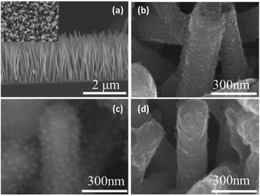
Fig. 1 shows SEM images of the as-prepared ZnO NW array, ZnO–CIS (ZC), ZnO–Ag (ZA) and ZAC nanostructures. A low-magnification side-view SEM image of the ZnO NW array on FTO is presented in Fig. 1(a), while the inset shows the top-view SEM image. Note that the ZnO NWs are about 150 nm in width and 2 μm in length with a highly vertical alignment. Fig. 1(b)–(d) display typical single nanowires of ZC, ZA and ZAC, respectively. It can be clearly seen that CIS or Ag NPs are distributed on the surface of the ZnO NWs.XRD spectra were measured to examine the crystalline structures of the ZAC samples. As shown in Fig. 2, as a comparison, the XRD pattern of the substrate (FTO) was measured at the same time. Besides the FTO, it can be seen that there are three sets of diffraction peaks for ZnO, Ag and CIS, respectively. Note that the sample lies on the test bench, and that the strongest peaks for ZnO are (101), (102), and (103). We can infer the ZnO NWs grew along the (001) direction with high orientation.29,30 The data shows a strong peak in the (111) direction is attributed to the synthesized Ag nanoparticles, consistent with a face-centered cubic (fcc) structure,30 which is an important property relating to the enhanced photo-catalytic activity of our ZAC sample. Another two diffraction peaks can be indexed to the (112) and (204) directions, reflecting the tetragonal crystal structure of CIS.31
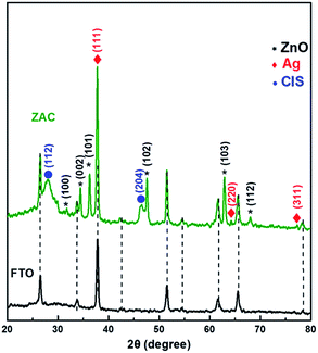 | ||
| Fig. 2 X-ray diffraction patterns for the ZAC sample and the substrate (FTO) (JCPDS no. 99-0111 for ZnO, 87-0598 for Ag, 27-0159 for CIS). | ||
The as-prepared ZAC nanostructures were further characterized using high resolution TEM (HRTEM) and EDX. Fig. 3(a) shows a low-magnification TEM image of ZnO decorated with Ag and CIS NPs. It’s clear that the ZnO nanowire is fully covered by CIS, which can effectively protect ZnO from photo-corrosion. In order to further analyze the micro-structures, a HRTEM image of the ZAC nanostructure is displayed in Fig. 3(b). Four sets of parallel lattice fringes were obtained easily. The spacing of 0.26 nm corresponds to the (002) plane of hexagonal ZnO, the 0.25 nm is attributed to the (004) plane of Ag nanoparticles and the 0.32 nm arises from the (112) plane of CIS NPs.17 Additionally, the HRTEM image also reveals a distinguished and coherent interface between the ZnO NWs, Ag nanoparticles and CIS NPs, demonstrating the formation of semiconductor–metal–semiconductor hetero-structures. From the above analysis, the ZAC nanostructure has been fabricated on the FTO substrate. Fig. 3(c) shows the corresponding EDX image of the sample, in which we can find the elements Zn, O, Ag, Cu, In and S.
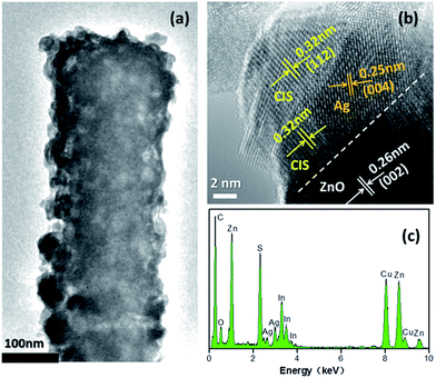 | ||
| Fig. 3 (a) A low-magnification TEM image of a Ag and CIS NP decorated ZnO NW, (b) a HRTEM image and (c) an EDX spectrum of the ZAC sample. | ||
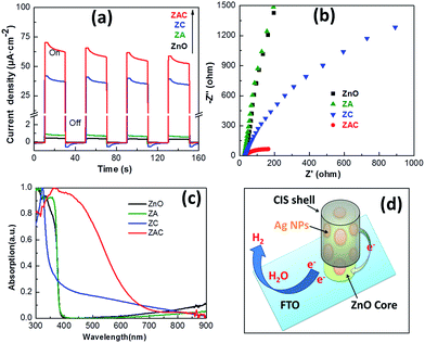
To better understand the roles of the ZnO NWs and the Ag and CIS NPs, photoelectrochemical (PEC) measurements were performed. The time courses of the photoresponses of the different sample electrodes with visible light switching on and off are depicted in Fig. 4(a), which are generally used to evaluate the electronic interactions among ZnO NWs, Ag NPs, and CIS NPs. As shown in Fig. 4(a), prompt and reversible photocurrent responses are achieved for each on/off cycle when the as-prepared ZAC sample serves as the working electrode. The sharp change between the on and off cycles indicates that the separation rate of photogenerated electron–hole pairs had increased due to the heterostructure built between the three components. In contrast, the photo-current of the ZnO sample shows a relatively slow response (the black line). Under the same conditions, the photocurrent density of ZAC (the red line) is about 100 times higher than that of pristine ZnO, while that of the ZC electrode (the blue line) is about 60 times higher, as shown in Fig. 4(a).
The significant enhancement of the photocurrent density originates from the charge separation occurring in the ZC and ZAC samples. It is worth noting that the photocurrent density of ZAC is higher than the sum of those of the ZC and ZA electrodes. Therefore, the deposition of Ag NPs on the surface of the ZnO NWs improves the photogenerated electron–hole separation because of the different conduction band alignment and Fermi level of ZnO and the Ag nanoparticles. In our system, it suggests that the Ag NPs can separate and collect the photogenerated electrons, leaving holes in CIS and consequently reducing the recombination rate of the photogenerated electrons and holes. After chemical deposition of the CIS NPs, the ZA NWs reveal further enhanced photocurrent generation, manifesting that the charge separation is further improved. Therefore, this hybrid ZAC nanostructure effectively promotes the overall charge separation efficiency. Furthermore, it is noteworthy that the photocurrent of the ZAC electrode maintains relative stability after four on–off light cycles. Meanwhile, Fig. 4(b) shows the EIS Nyquist plots of the ZAC samples with light irradiation. The smaller circles indicate that more effective and faster electron–hole separation occurred under visible light irradiation. It is obvious that there is a huge improvement of the charge separation efficiency between the ZC and ZAC samples, which means that the Ag NPs play an important role in this system.
Diffusive reflectance spectra (from 300 nm to 900 nm) of the samples were also measured and are shown in Fig. 4(c). The black line (ZnO) and the green line (ZnO/Ag) are typical semiconductor absorption spectra, in which the band gap of the ZnO NWs was revealed to be approximately 3.21 eV (386 nm). The huge absorbance of ZAC proves that the Ag NPs and CIS NPs have a synergistic effect. Thus, a scheme of the electronic transmission is described in Fig. 4(d). Under sunlight, the electrons in the CIS NPs were activated from the valence band to the conduction band. Attributed to the good electrical conductivity of the Ag NPs, the electrons were quickly transferred to the conduction band of ZnO. Then the electrons were collected on FTO and the hydrogen evolution occurred.
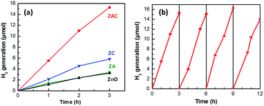
A full-spectrum solar simulator was used as the excitation source, placed in a Pyrex glass container with 100 mL water. 3.15 g Na2SO3 and 8.4 g Na2S were added to the water as sacrificial reagents, and the anodic reaction generating O2 from H2O did not occur. The ZnO NWs, Ag NP assisted ZnO NWs, CIS NP assisted ZnO NWs and Ag and CIS NP assisted ZnO NWs on one piece of FTO (2 × 4 cm2) were tested in turn for their photo-catalytic H2 generation in this system, as shown in Fig. 5(a). Compared with pure ZnO NWs, the catalytic production of H2 by the Ag or CIS NP assisted ZnO NWs was just slightly increased, however, it was significantly enhanced by the ZAC nanostructures. XPS was conducted (see the ESI Fig. S1†), demonstrating the existence of Ag(0).32,33 From these results, we can conclude that Ag and CIS NPs play a synergistic role, serving as co-catalysts. The Ag NPs can improve the transport of photogenerated electrons on the surface of CIS under visible light (Fig. 4(b)), reducing the recombination rate of the photogenerated electron–hole pairs. As such, the Ag nanoparticles make a pronounced charge separation occur at the ZnO/CIS interfaces. Furthermore, the type II heterostructure between ZnO and CIS with an appropriate band alignment not only increases the adsorption but further enhances the photogenerated electron–hole separation. In this system, the photogenerated electrons were transferred and collected on ZnO nanorods for H2 evolution (Fig. 4(d)). Meanwhile, the holes were consumed by the sacrificial reagent. The result indicates that any component in this system is indispensable for achieving a high photo-catalytic efficiency. On average, nearly constant H2 evolution by ZAC under light illumination has been observed for at least 12 h, as shown in Fig. 5(b). The yield of H2 after a 12 h reaction time had reached 60 μmol, and more importantly, this system also showed the stability after light irradiation from the post irradiation. For ZAC, the rate of H2 production can reach up to 0.625 μmol cm−2 h−1, about 5 times that of pure ZnO NWs. It is expected that this rate may be further enhanced several times by increasing the length of the ZnO NWs and controlling the distribution of CIS and Ag on the ZnO NWs.22
Conclusions
In summary, Ag and CuInS2 NPs are loaded onto ZnO NW arrays that are prepared on extensive substrates. With the sensitization of the CuInS2 NPs, the increase in the photocurrent is about 60 fold compared to pure ZnO. With the synergistic effect of the Ag and CuInS2 NPs, the increase in the photocurrent is about 100 fold. The enhancement of hydrogen evolution is more than 5 fold, as well as the relative stability. Furthermore, compared with the traditional pulverous catalysts such as CdTe, CdS and ZnSe, the ZnO/Ag/CuInS2 system is environmentally friendly and the growth on a substrate can improve recyclability in an aqueous solution because it is easily entirely removed from the aqueous solution. Notably, the noble metal nanoparticles introduced into the traditional binary semiconductor composite provide a new strategy for designing new photo-catalysts for the decomposition of water, driven by visible light.Acknowledgements
This work was supported by the 973 Program of the Ministry of Science and Technology of China (No. 2012CB934103), the 100-Talents Program of the Chinese Academy of Sciences (No. Y1172911ZX), the National Natural Science Foundation of China (No. 21373065 and 61474033) and the Beijing Natural Science Foundation (No. 2144059).References
- M. D. Hernández-Alonso, F. Fresno, S. Suárez and J. M. Coronado, Energy Environ. Sci., 2009, 2, 1231 Search PubMed.
- N. Liu, C. Schneider, D. Freitag, M. Hartmann, U. Venkatesan, J. Muller, E. Spiecker and P. Schmuki, Nano Lett., 2014, 14, 3309–3313 CrossRef CAS PubMed.
- W. Zhao, Z. Ai, J. Dai and M. Zhang, PLoS One, 2014, 9, e103671 Search PubMed.
- X. Chen, L. Liu, P. Y. Yu and S. S. Mao, Science, 2011, 331, 746–750 CrossRef CAS PubMed.
- J. Huang, Z. Yin and Q. Zheng, Energy Environ. Sci., 2011, 4, 3861 CAS.
- Y. Tak, S. J. Hong, J. S. Lee and K. Yong, J. Mater. Chem., 2009, 19, 5945 RSC.
- G. Wang, X. Yang, F. Qian, J. Z. Zhang and Y. Li, Nano Lett., 2010, 10, 1088–1092 CrossRef CAS PubMed.
- Z. Wang, H. Yin, C. Jiang, M. Safdar and J. He, Appl. Phys. Lett., 2012, 101, 253109 CrossRef PubMed.
- Z. Wang, X. Zhan, Y. Wang, M. Safdar, M. Niu, J. Zhang, Y. Huang and J. He, Appl. Phys. Lett., 2012, 101, 073105 CrossRef PubMed.
- J. Xu, X. Yang, H. Wang, X. Chen, C. Luan, Z. Xu, Z. Lu, V. A. Roy, W. Zhang and C. S. Lee, Nano Lett., 2011, 11, 4138–4143 CrossRef CAS PubMed.
- Y. Wang, Q. Wang, X. Zhan, F. Wang, M. Safdar and J. He, Nanoscale, 2013, 5, 8326–8339 RSC.
- X. Wang, H. Zhu, Y. Xu, H. Wang, Y. Tao, S. Hark, X. Xiao and Q. Li, ACS Nano, 2010, 4, 3302–3308 CrossRef CAS PubMed.
- S. Khanchandani, S. Kundu, A. Patra and A. K. Ganguli, J. Phys. Chem. C, 2013, 117, 5558–5567 CAS.
- X. Zhan, Q. Wang, F. Wang, Y. Wang, Z. Wang, J. Cao, M. Safdar and J. He, ACS Appl. Mater. Interfaces, 2014, 6, 2878–2883 CAS.
- Y. Wang, Z. Wang, S. Muhammad and J. He, CrystEngComm, 2012, 14, 5065 RSC.
- M. Ajili, M. Castagné and N. Kamoun Turki, J. Lumin., 2014, 150, 1–7 CrossRef CAS PubMed.
- J. Ran, J. Zhang, J. Yu, M. Jaroniec and S. Z. Qiao, Chem. Soc. Rev., 2014, 43, 7787–7812 RSC.
- Y. Choi, M. Beak and K. Yong, Nanoscale, 2014, 6, 8914–8918 RSC.
- Y. Li, Z. Liu, Y. Wang, Z. Liu, J. Han and J. Ya, Int. J. Hydrogen Energy, 2012, 37, 15029–15037 CrossRef CAS PubMed.
- F. Shen, W. Que, Y. He, Y. Yuan, X. Yin and G. Wang, ACS Appl. Mater. Interfaces, 2012, 4, 4087–4092 CAS.
- K. Lee, R. Hahn, M. Altomare, E. Selli and P. Schmuki, Adv. Mater., 2013, 25, 6133–6137 CrossRef CAS PubMed.
- C. Duan, H. Wang, X. Ou, F. Li and X. Zhang, ACS Appl. Mater. Interfaces, 2014, 6, 9742–9750 CAS.
- Z. Bian, T. Tachikawa, P. Zhang, M. Fujitsuka and T. Majima, J. Am. Chem. Soc., 2014, 136, 458–465 CrossRef CAS PubMed.
- J. S. DuChene, B. C. Sweeny, A. C. Johnston-Peck, D. Su, E. A. Stach and W. D. Wei, Angew. Chem., Int. Ed., 2014, 53, 7887–7891 CrossRef CAS PubMed.
- J. Han, W. Qiu and W. Gao, J. Hazard. Mater., 2010, 178, 115–122 CrossRef CAS PubMed.
- M. A. Fox and M. T. Dulay, Chem. Rev., 1993, 93, 341–357 CrossRef CAS.
- P. Spathis and I. Poulios, Corros. Sci., 1995, 37, 673–680 CrossRef CAS.
- R. Zhu, W. Zhang, C. Li and R. Yang, Nano Lett., 2013, 13, 5171–5176 CrossRef CAS PubMed.
- S. A. Ansari, M. M. Khan, J. Lee and M. H. Cho, J. Ind. Eng. Chem., 2014, 20, 1602–1607 CrossRef CAS PubMed.
- D. H. Yoo, T. V. Cuong, V. H. Luan, N. T. Khoa, E. J. Kim, S. H. Hur and S. H. Hahn, J. Phys. Chem. C, 2012, 116, 7180–7184 CAS.
- H. Zhong, S. S. Lo, T. Mirkovic, Y. Li, Y. Ding, Y. Li and G. D. Scholes, ACS Nano, 2010, 4, 5253 CrossRef CAS PubMed.
- R. Bird and P. Swift, J. Electron Spectrosc. Relat. Phenom., 1980, 21, 227–240 CrossRef CAS.
- L. Liu, D. T. Pitts, H. Zhao, C. Zhao and Y. Li, Appl. Catal., A, 2013, 467, 474–482 CrossRef CAS PubMed.
Footnotes |
| † Electronic supplementary information (ESI) available. See DOI: 10.1039/c5ra14188e |
| ‡ Z. Cheng and X. Zhan contributed equally to this work. |
| This journal is © The Royal Society of Chemistry 2015 |

