Pankaj Sharmaa,
Rohit Singha,
Vishnu Awasthia,
Sushil K. Pandeyb,
Vivek Garga and
Shaibal Mukherjee*a
aHybrid Nanodevice Research Group (HNRG), Indian Institute of Technology, Indore 453446, India. E-mail: shaibal@iiti.ac.in; Fax: +91-731-2361482; Tel: +91-732-4240704
bDepartment of Electrical Engineering, Indian Institute of Technology Bombay, Mumbai 400076, India
First published on 5th October 2015
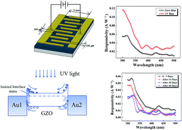
Ga-doped ZnO (GZO) based ultraviolet photodetectors (PDs) were fabricated by dual ion beam sputtering with a metal–semiconductor–metal structure. The room-temperature operable PD demonstrated responsivity of 58 mA W−1 at zero bias, which is 15 times larger than that reported on similar material grown by a different physical vapour deposition process, with internal and external quantum efficiency values of ∼22.5% and 37.4%. The unbiased photodetection is attributed to the tunnelling of electrons due to heavy doping of GZO and built-in electric field due to different barriers at the two metal semiconductor contacts. The asymmetry in the electrodes was investigated by temperature-dependent current–voltage measurements.
Since almost all kind of photodetectors requires external supply for their operation, it is highly desired to have PDs based on self-powered mechanism. These PDs are critical in terms of energy saving point of view and are preferred for long-term monitoring of air-pollution and wastewater. To the best of our knowledge the reports on unbiased photoresponse of ZnO based MSM photodetectors are still rare. Instead, recently Bai et al. and Ni et al. have reported similar results, for ZnO based heterostructures.13,14 In this work, we discuss the phenomenon of zero bias photoresponse of GZO thin film PD, grown by DIBSD system, by investigating the electron transport mechanism through Au/GZO interface. In our GZO based photodetector, the internal quantum efficiency (IQE) at zero bias was as high as 37% with ultraviolet to visible rejection ratio of more than five orders.
![]() | ||
Fig. 1 (a) XRD patterns of GZO films grown at different Tg, (b) carrier concentration, mobility, and resistivity of GZO films, (c) SIMS depth profile of as-grown GZO film. |
Sample (device) | Growth temperature (°C) | Peak position 2θ (degree) | FWHM (degree) | Grain size (nm) | EQE (%) | IQE (%) |
---|---|---|---|---|---|---|
S2 (D2) | 200 | 34.05 | 0.32 | 27.1 | 6.11 | 10.18 |
S3 (D3) | 300 | 34.3 | 0.2 | 43.4 | 22.5 | 37.41 |
S4 (D4) | 400 | 34.25 | 0.36 | 24.1 | 3.21 | 5.35 |
S5 (D5) | 500 | 34.32 | 0.3 | 28.9 | 1.01 | 1.68 |
S6 (D6) | 600 | 34.27 | 0.68 | 12.7 | 0.99 | 1.65 |
The Hall measurement exhibited n-type conduction for all GZO films. This n-type conduction is due to Ga incorporation into GZO where Ga will occupy Zn sites and be ionized into Ga3+. This process supplies one free electron to the conduction band for each Ga atom added. Fig. 1(b) shows the carrier concentration, mobility, and resistivity of GZO films as a function of Tg. The electrical resistivity of GZO film decreased marginally when Tg reached 300 °C and afterwards the resistivity increased sharply with higher Tg. A minimum resistivity value of 5.3 × 10⁻⁴ Ω cm is obtained at 300 °C. Similarly, the carrier concentration demonstrated an enhancement19 up to 300 °C and then reduced gradually with further increase in Tg. The trend of variation of electrical resistivity and carrier concentration was guided by the crystallinity of GZO films, as depicted in Fig. 1(a).19 However, carrier mobility exhibited an initial increase with increasing Tg from 200 to 400 °C and then decreased sharply at 500 °C. This decay in mobility, with carrier concentration of ∼1020 cm−3, may have been caused by ionized impurity scattering.20 As it is well known that mobility in heavily doped ZnO is controlled by various factors such as dislocations, grain boundary scattering, ionized impurity scattering, and carrier concentration etc.,20 a sharp increase in mobility at 600 °C may be correlated to lesser scattering effect with comparatively low electron concentration at 600 °C.21 The depth profile of the main elements in an as-grown GZO film (S3) is shown in Fig. 1(c). It is evident that Ga has been clearly detected, and its concentration profile is quite flat throughout the film depth.
Shadow masking technique was deployed to fabricate MSM-type device structure using a metal interdigitated mask. The electrode fingers were 5 mm long, 100 μm wide, and the spacing between two adjacent fingers were 200 μm. The schematic diagram of the fabricated device is shown in Fig. 2(a). Fig. 2(b) shows the absorption spectra of sample S3 that clearly depicts that the layer has a strong absorption to photons with wavelength shorter than 370 nm, while it is almost transparent to those with wavelength longer than 400 nm. The spectral response measurements of PD, as shown in Fig. 2(c), were carried out from 300 to 500 nm. The photo-responsivity was measured in unbiased (zero bias) mode as well as applying a small positive bias voltage, 1 V at room temperature. It is observed that the device D3 has the highest responsivity of 58 mA W−1 at zero bias, which is ∼15 times and 3 times larger than that reported in ref. 8 and 22, respectively. The response peak is centered on 325 nm and a cut-off wavelength around 370 nm corresponding to the band gap energy of GZO films. Table 2 compares the various reports on zero bias photo response from available literature.8,22,23 Responsivity (Ri) of the photodetector can be expressed as Ri = ηg(qλ/hc),9 where λ is wavelength, q is electronic charge, h is the Plank's constant, c is light velocity in free-space, η is EQE, and g is the gain. An increase in the quantum efficiency was observed on application of external bias exhibiting the photoconductive gain. Table 3 shows the values of absorption edge wavelength, as calculated using the inset of Fig. 2(b), and peak photoresponse wavelength, as evaluated from Fig. 2(c), of all GZO samples and corresponding devices. It is clear that the trend of variation of photoresponse peak wavelength is governed by that of absorption peak wavelength. Fig. 2(d) shows the spectral response of device D3 at zero and 1 V bias, respectively. Device IQE was determined by normalizing the EQE as IQE = EQE/(1 − R),24 where R is the measured reflectance of the GZO layer. While the EQE at zero bias was measured to be ∼22.5%, it reached to 48% at 1 V bias with an average photocurrent of 23 mA. A significantly higher value of IQE at zero bias was calculated to be 37.4%. On further increase in applied bias, the photocurrent reaches saturation and the measurement was limited by instrument capability. Moreover, photosensitivity measurements of the GZO PDs were performed by turning the continuous UV illumination at 325 nm ON and OFF at an applied bias of 1 V. Fig. 2(e) shows the photocurrent rise and decay as a function of time at an applied bias of 1 V. The device was kept in dark for 12 hours to stabilize and then exposed to UV radiation for 25 s. The rise time is defined as the time needed to reach 90% from 10% of the maximum photocurrent while the fall time is the time needed to reach 10% from 90% of the maximum photocurrent.6 From Fig. 2(e), the values of rise time of 806 ms and fall time of 54 s were obtained for the GZO UV photodetector. The photosensitivity (S) can be expressed as S = (Ilight − Idark)/Idark,11 where Ilight and Idark are the light and dark current with and without UV illumination, respectively. The values of photosensitivity and on/off ratio (Ilight/Idark) for device D3 were calculated to be 0.076 and 1.076, respectively. In order to assess the feasibility of using the MSM PD for practical applications, the responsivity measurement at zero bias voltage is conducted, as demonstrated in Fig. 2(f), for different intervals: (a) first 7 days, (b) 14 days, (c) 30 days, and (d) 60 days after device fabrication. It should be noted that the device was kept in normal ambient condition without having any passivation layer on top of it during the photo stability measurement.
Sample (device) | Absorption edge (nm) | Peak photoresponse wavelength (nm) |
---|---|---|
S2 (D2) | 356 | 355 |
S3 (D3) | 325 | 325 |
S4 (D4) | 340 | 365 |
S5 (D5) | 351 | 355 |
S6 (D6) | 363 | 375 |
In order to get a better understanding of the carrier transport phenomenon at the Au/GZO interface, one must recognize which transport process plays a dominant role in our MSM PD. Various models have been proposed to explain the excess leakage current through Au/GZO Schottky barrier but in general, the total current constitutes of both thermionic emission and tunnelling component. Assuming that thermionic emission is predominant, the reverse saturation current of a diode with tunnelling is given as,25
I = Is![]() | (1) |
E00 = (qħ/2)(ND/m*εs)1/2 | (2) |
In order to investigate the high photoresponse at zero applied bias, a model based on thin surface barrier27 with asymmetric electrodes28,29 is assumed. It is well known that surface barrier lowering occurs at metal–semiconductor interface25,30 due to the presence to donor defect states, resulting in reduction of Schottky barrier width such that the electron can easily tunnel across the junction, as confirmed by above calculation. To establish the dissimilar characteristic of identically deposited Au electrodes on GZO films, I–V measurements for both forward and reverse bias voltages were performed in temperature ranging from 80 to 300 K. Indium contact was realized on top of GZO surface to form a perfect ohmic contact. Fig. 3(a) shows the temperature dependent ln(I)–V curves for Au1/GZO/In while Fig. 3(b) displays the temperature dependent ln(I)–V curves for Au2/GZO/In, where Au1 and Au2 are two Au contacts on GZO films, respectively. It is clearly observed that the current for Au1/GZO/In is temperature independent confirming the tunnelling of carriers, whereas current increases for Au2/GZO/In contacts demonstrating a relatively weaker Schottky behaviour. Moreover, Fig. 3(c) depicts I–V characteristics of both Au contacts at 80 and 300 K illustrating the clear inhomogeneity in the identically deposited electrodes.
The asymmetrical behaviour of Au electrodes may have been originated from dissimilar accumulation of surface/donor defect states at the interface of Au/GZO junction.31 The variation in the generation of such interface defect states might have been resulted due to dissimilar surface damage triggered by sputtering of Au electrodes on GZO films. Based on the experimental results and analysis, the energy band diagram for GZO-based MSM PD in zero biased conditions is shown in Fig. 3(d). Under the UV illumination, the photogenerated electrons tend to move towards the GZO while the photogenerated holes move towards the metal contacts. The interface states may be ionized by the accumulation of these hot carriers, modifying the local potential, which has been displayed by the band bending at interface of Fig. 3(d). In order to verify the assumed hypothesis, the Schottky barrier heights for two Au contacts is calculated using the equation I = AA*T2exp(−qΦb/KBT) where I is the current through the Schottky barrier, A is the contact area, A* is Richardson's coefficient, T is absolute temperature, and qΦb is the barrier height.32 The values of qΦb, as measured from the forward biased region in Fig. 3(c) at room temperature, show very little difference for Au1/GZO/In (0.342 eV) and Au2/GZO/In (0.345 eV). However, in the reverse bias region this difference is comparatively larger with 0.344 eV for Au1/GZO/In and 0.352 eV for Au2/GZO/In. Liu et al. have reported similar observations in ZnO film with electron concentration of order of 1 × 1017 cm−3, due to trapping of carriers in the presence of trap states. In this case, GZO films having an electron concentration ≥ 1020 cm−3 the phenomenon is attributed to the ionization of interface states33 on exposure to UV light. This ionization of interface states in highly conducting films enhances the free electron charge in conduction band and thereby shifting the quasi Fermi level to higher energies34 resulting in lowering of barrier height and enhanced carrier tunnelling. There can be two-fold explanations behind higher zero bias photoresponse from our MSM-based UV PD as compared to others in literature, as shown in Table 2: (1) good crystalline quality of GZO film deposited by DIBSD system, (2) high electron concentration of the order of 1021 cm−3 and a very low electrical resistivity allow a significantly larger amount of photocurrent to pass between the electrodes under the exposure of UV illumination. The physical transport of electrons dominated by tunnelling under the effect of asymmetric Schottky barrier enables the device to operate at zero bias voltage.
This journal is © The Royal Society of Chemistry 2015 |