DOI:
10.1039/C5RA13884A
(Paper)
RSC Adv., 2015,
5, 74126-74131
Facile synthesis of oleylamine-capped silver nanowires and their application in transparent conductive electrodes†
Received
15th July 2015
, Accepted 24th August 2015
First published on 24th August 2015
Abstract
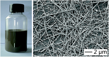
We report a facile method for the synthesis of oleylamine-capped silver (Ag) nanowires in high purity. For the first time, Ag nanowires could be produced in high purity via a simple one-pot approach in a hydrophobic phase. The success of this synthesis relies on the use of Cu2+ to mediate the reduction of silver bromide (AgBr) by oleylamine at an elevated temperature, which promoted the high-yield formation of Ag products with a wire-like shape. These Ag nanowires were washed and deposited on PET films to form a transparent conductive electrode (TCE), which showed a sheet resistance of 34.0 Ω sq−1 and an optical transmittance of 70–80% at visible wavelengths. In addition to TCEs, these nanowires could also find important applications in the fields of conductive ink, and wearable electronics, among others.
Introduction
One-dimensional metallic nanocrystals have attracted significant research attention in the past few decades due to their unique electronic, optical, thermal, and catalytic properties.1–13 Among these metals, silver (Ag) nanowires has been an area of active research because Ag exhibits the highest electrical and thermal conductivities.14–21 Owing to these merits, Ag nanowires are attractive building blocks for applications in photonic, electronic, and sensing fields. For example, Ag nanowires have been considered as one of the most promising candidates to replace tin-doped indium oxide (ITO) to serve as the transparent conductive electrode (TCE) for the next-generation display devices with flexible characteristics.22–27
Thanks to research efforts contributed by many groups, several synthetic approaches have been proposed and validated for the fabrication of metallic nanowires with reasonable yields (e.g., template assisted in-plane growth of nanowires, and electric field assisted growth of nanowires, among others).28–31 Compared to physical routes, wet-chemical synthesis exhibited tremendous advantages, such as being template-free, low cost, easy to scale up, and having mild reaction conditions, among others.32–39 Take silver for example: as a pioneer in this field, Xia and coworkers demonstrated that high-quality Ag nanowires could be obtained by dropwisely adding ethylene glycol solutions of AgNO3 and poly(vinylpyrrolidone) (PVP) at an elevated temperature.40–43 This method was further improved and optimized to overcome several drawbacks, such as long reaction times, low wire-to-particle yields, irregular wire morphologies, and low aspect ratios.44,45 In addition to the use of ethylene glycol as the solvent, other reagents were also employed.46–48 For example, Murphy and coworkers reported the synthesis of crystalline silver nanowires in water, in the absence of a surfactant or polymer to direct nanoparticle growth. Wong and coworkers reported a facile preparation method for Ag nanowires with uniform diameters of 60 ± 2 nm where glycerol was used as the solvent.48 All these reports have contributed to the development of synthetic protocols for Ag nanowire fabrication.
Despite these successful demonstrations, it is worth noting that there has been no report about the synthesis of Ag nanowires in a hydrophobic phase yet. When the Ag nanowires were capped with hydrophilic molecules, it is difficult to mix and suspend them with hydrophobic materials (e.g., oil, resin, among others) homogeneously, which limits their further applications. To this end, it is highly desirable to develop a convenient approach for the production of Ag nanowires capped with hydrophobic molecules and extend their use to more applications in hydrophobic systems.
The use of metallic cations to mediate the shape-controlled synthesis of noble metals has aroused enormous research attention recently.49–51 Typically, the addition of a secondary metal precursor in a trace amount in the synthesis, which can react with the major metal through specific adsorption or coordination, changes the growth pattern of the major metal. Take copper cations for example: Xia and coworkers reported the use of Cu2+ to reduce the amount of free Ag+ during the formation of initial seeds, and to scavenge adsorbed oxygen from the surface of the seeds once formed in the synthesis of Ag nanowires.45 Xie and coworkers synthesized Au–Pd alloyed nanocrystals with a special hexoctahedral (HOH) shape via a Cu2+-mediated reaction.52 For these demonstrations, the roles of copper cations are considered to influence the reaction kinetics and/or vary the crystal plane growth via underpotential deposition.
Herein, we describe a facile route for the fabrication of high-purity Ag nanowires capped with hydrophobic molecules, oleylamine (OAm). The success of this synthesis relies on the use of copper chloride (CuCl2) to mediate the reduction of silver bromide (AgBr) by OAm at an elevated temperature. To the best of our knowledge, it is the first time that hydrophobic molecule-capped Ag nanowires have been produced in high purity via a simple one-pot method. To understand the formation mechanism, we monitored the process by terminating the reaction and taking out an aliquot for SEM imaging at different stages. In addition, the amount of CuCl2, reaction temperature, and type of Ag precursor were also evaluated to reveal their impacts on the final product morphology. These oleylamine-capped Ag nanowires were then washed and deposited on PET films to form a TCE, which showed a sheet resistance of 34.0 Ω sq−1 and an optical transmittance of 70–80% at visible wavelengths. This work provides a feasible strategy to synthesize one-dimensional Ag nanomaterials in a hydrophobic phase, which can potentially be extended to other noble metals.
Experimental
Materials
Silver bromide (AgBr, ≥99.0%), anhydrous copper chloride (CuCl2, 99.99%), oleylamine (OAm, 80–90%), and hexane were all obtained from Aladdin Industrial Inc. and used as received. Silver chloride (AgCl, ≥99.5%) and silver nitrate (AgNO3, ≥99.8%) were obtained from Sinopharm Chemical Reagent Co., Ltd and used as received. CuCl2–OAm solution (0.3 g L−1) was prepared by mixing 3 mg of CuCl2 in 10 mL of OAm at 60 °C for 10 min and cooled down to room temperature naturally.
Synthesis of OAm-capped Ag nanowires
For a typical synthesis, 600 mg of AgBr, 0.1 mL of CuCl2–OAm solution (0.3 g L−1), and 30 mL of oleylamine were added to a 250 mL round bottle flask to which a stir bar was added. The concentration of Ag ions in the reaction system was 106.5 mM. The flask was then suspended and heated using a heating mantle under magnetic stirring (300 rpm). The reaction was allowed to continue for 6 hours and was then quenched by cooling the flask in a room-temperature water bath. The products were then centrifuged at 6000 rpm for 10 minutes, washed with hexane three times, and stored in hexane for further use and characterization.
Preparation of TCE films composed of Ag nanowires
For a typical process, the as-prepared hexane solution containing Ag nanowires was directly applied onto a piece of PET film. A Meyer rod was used to make sure the film with homogeneously coated with the solution. Then the films were dried in air at room temperature for further use and characterization.
Instrumentation
Scanning electron microscopy (SEM) images were captured using an Ultra Plus microscope operated at 3.0 kV (Zeiss, Oberkochen, Germany). The samples were prepared by dropping suspensions of nanowires onto Cu foils. High-resolution TEM (HRTEM) images and electron diffraction patterns were obtained using a field-emission JEM-2100F microscope operated at 200 kV (JEOL, Tokyo, Japan). The samples were prepared by dropping suspensions of nanowires onto carbon-coated Cu grids and dried under ambient conditions. X-ray diffraction (XRD) patterns were recorded using a diffractometer with filtered Cu Kα radiation at 0.154 nm. All extinction spectra were recorded using a Persee TU-1900 UV-vis-NIR spectrometer (Purkinje General Instrument, Beijing, China). Sheet resistance was measured using the four-probe method.
Results and discussion
In a standard process, oleylamine solution containing AgBr and CuCl2 was heated at 160 °C for 6 hours and cooled down to room temperature naturally. Grey precipitates were observed at the bottom of the flask, indicating the formation of Ag nanowires. As shown in Fig. 1A–C, the resultant products exhibited a wire-like shape (33.8 ± 2.6 nm in width and 15 ± 7 μm in length) in high purity. It is worth pointing out that such Ag nanowires could be routinely synthesized in high purity (>98%) without involving any additional purification/separation processes. To further confirm their structure and shape, we also performed a series of measurements in addition to SEM and TEM imaging, including HRTEM, ED, EDS, and XRD. The HRTEM image (Fig. 1D) taken from an individual Ag wire shows a continuous fringe pattern with a spacing of 0.236 nm, which could be indexed to the {111} reflection of face-centered cubic (fcc) Ag. The corresponding ED pattern (the inset in Fig. 1C) has more than one set of diffraction spots, suggesting a twinned structure. Fig. S1† shows an XRD pattern of the Ag nanowires, where the diffraction peaks occurring at 38.1°, 44.3°, 64.5°, and 77.5° are indexed as (111), (200), (220), and (311) facets, being in good consistency with an fcc Ag crystalline structure (JCPDS 04-0783). No peak for other crystal types was observed. The sharp diffraction peaks indicated the sample had a high crystallinity. The EDS pattern confirmed that there is no other metallic element involved in the product (Fig. S2†). Taken together, we can conclude that the as-obtained Ag products had a twinned structure, together with a wire-like shape.
 |
| Fig. 1 Characterization of Ag nanowires: (A–B) SEM images; (C) TEM and (D) HRTEM images. The inset in (C) shows the electron diffraction pattern. | |
To understand the formation mechanism, we monitored the reaction by terminating the synthesis at different periods and taking out aliquots for SEM imaging. As shown in Fig. 2A, at t = 1 h, the products were predominantly nanocubes with a typical size of 168 nm. It is worth noting that these nanocubes were not stable and exhibited noticeable shape variation upon SEM electron irradiation, suggesting they are likely to be composed of AgBr instead of Ag due to their photosensitivity. To verify this, we collected those particles and performed analysis using XRD. As shown in Fig. S3,† their diffraction patterns could be identified as AgBr (JCPDS 79-0149) rather than Ag, which confirmed their composition. Previous studies indicated that during the synthesis of Ag nanowires, the formation of silver halide nanocubes could induce the heterogeneous nucleation of metallic Ag upon their surfaces.46,53 Then, Ag nanowires would subsequently grow from these nucleation sites. When the reaction was continued to t = 2 h, wire-like products began to appear but the yield was still low (Fig. 2B). The percentage of nanowires significantly increased as reaction proceeded to t = 4 h (Fig. 2C). An even longer reaction period had little impact on the yield of wire-like products (Fig. 2D). Based on these results, the reaction pathway was schematically illustrated in Fig. S4.†
 |
| Fig. 2 SEM images of an aliquot taken out from the reaction system at (A) t = 1 h; (B) t = 2 h; (C) t = 4 h; and (D) t = 12 h. The inset in (A) shows typical AgBr nanocubes. | |
In the current synthesis, CuCl2 was found to be necessary for Ag nanowire formation. To probe the role of Cu ions in this synthesis, a set of control experiments were conducted with the addition of different amounts of CuCl2. As shown in Fig. 3A and B, if no or a lower amount of CuCl2 was present in the reaction solution, the purity of the final products was not satisfactory. Only part of the final products was nanowire and large quantities of nanoparticles could be observed. In contrast, the yield of Ag nanowires remained unchanged when the concentration of CuCl2 was increased (Fig. 3C and D). These results indicated that a sufficient supply of CuCl2 was necessary for the formation of wire-like products in high purity. Generally, in order to achieve high-yield formation of Ag nanowires, particles with a penta-twinned structure should survive and dominate the seeds formed in the initial stages. In our case, Cu(I), generated in situ from the reduction of Cu(II), could effectively scavenge any adsorbed atomic oxygen from the Ag seeds, thus dampening the oxidative etching strength and protecting the penta-twinned particles from being etched.45,54,55 In other words, without sufficient Cu ions, it is highly possible that those penta-twinned particles could not survive in the initial stages. As a result, Ag nanocrystals with other crystallinities may appear as final products, which make the percentage of Ag nanowires lower. In short, the concentration of CuCl2 in the system could significantly influence the oxidative etching strength of Ag and thus the yield of penta-twinned Ag nanowires.
 |
| Fig. 3 The effect of CuCl2 amount on product morphologies. SEM images of products obtained using the standard procedure, except that the amount of CuCl2 was tuned from 0.03 mg in the standard procedure to (A) 0, (B) 0.01, (C) 0.5, and (D) 2 mg, respectively. The molar ratio of CuCl2 to Ag was (A) 0, (B) 1 : 42 818, (C) 1 : 856.37, and (D) 1 : 142.73, respectively. | |
We also evaluated the effect of the type of Ag precursor on the product morphology. As shown in Fig. 4, when the Ag precursor, AgBr, was replaced by AgNO3 and AgCl, the resultant products no longer exhibited the wire-like shapes. Instead, they were predominately polyhedral particles (Fig. 4A) and porous spheres with hollow interiors (Fig. 4B), respectively. These results indicated the anions involved with the Ag precursor can cause a significant change to the morphology of the final product. Compared to AgBr/Ag, the standard potentials of Ag+/Ag and AgCl/Ag are much higher (AgCl/Ag, 0.2223 V; Ag+/Ag, 0.7996 V; AgBr/Ag, 0.07133 V). The reduction rate would be accelerated when AgBr was replaced by either AgCl or AgNO3. As a result, variation of Ag precursor can significantly cause a change of the reaction kinetics, which may impact the nucleation and growth pattern and thus the morphology of the final products.
 |
| Fig. 4 The effect of Ag precursor on product morphologies. SEM images of products obtained using the standard procedure, except that the AgBr was replaced by (A) AgNO3 and (B) AgCl, respectively. | |
The current synthesis involved the use of AgBr, anhydrous CuCl2, and oleylamine. At an elevated temperature, oleylamine can serve as both the solvent and the reductant to reduce the Ag+ species to zero-valent Ag.56–59 As a result, the reaction temperature played an important role in influencing the reaction kinetics. To evaluate the effect of reaction temperature on product morphologies, we conducted a set of control experiments. Fig. 5 shows SEM images of the products obtained using the standard procedure except that the reaction temperature was changed. In particular, as reaction temperature was changed from 160 °C to 140, 170, 180, and 200 °C, the resultant products no longer exhibited the wire-like shape in high yield. In contrast, they were predominantly a mixture of wires and particles with various shapes. As indicated in the discussion above, the synergetic effect of oxidative etching and crystal growth played an important role in the formation of Ag nanowires in high purity. When the temperature was altered, the oxidative etching strength would be either enhanced or dampened. Since the amount of oxygen scavenger, CuCl2, was kept unchanged, different types of seeds may survive in the initial stages and thus the percentage of those five-fold twinned seeds may become lower. In short, the results of these control experiments showed that an appropriate reaction temperature was essential for the formation. Either higher or lower temperature may cause the change of oxidative etching strength, which led to the variation of crystallinities and shapes of the final products.
 |
| Fig. 5 The effect of reaction temperature on product morphologies. SEM images of products obtained using the standard procedure, except that the reaction temperatures were changed to (A) 140, (B) 170, (C) 180, and (D) 200 °C, respectively. | |
We washed the as-prepared oleylamine-capped Ag nanowires and deposited these nanowires onto PET films to test their performance as a TCE (Fig. 6A and B). As shown in Fig. 6C, by varying the concentration of Ag nanowire suspensions, a series of Ag nanowire films with different thicknesses on PET films have been prepared. The variation of concentration and thus thickness modifies the light transmittance of the films from 30–40% to approaching 90%. Simultaneously, their sheet resistance increases from 3.22 to 53.5 ohm sq−1, which means they have an extremely high conductivity level. This conductivity level satisfies the industrial requirements well and compares with Ag nanowire network electrodes documented in the literature.
 |
| Fig. 6 (A and B) Pictures of (A) a bottle of oleylamine-capped Ag nanowires suspended in hexane and (B) a piece of PET film coated with the as-prepared Ag nanowires. (C) UV/vis transmission spectra of Ag nanowire films on PET with controlled transparency. The resistance decreased from 53.5 to 3.22 ohm sq−1 with the decrease of transparency. | |
Conclusions
In summary, oleylamine-capped Ag nanowires have been successfully prepared in high purity via a simple one-pot approach. With the addition of CuCl2, the reduction of AgBr by oleylamine at an elevated temperature was found to promote the formation of Ag nanowires in high yield. By monitoring the reaction, we found that AgBr nanocubes were formed in the early stage, which then served as the sites for heterogeneous nucleation and thus the formation of Ag nanowires. The amount of CuCl2, type of Ag precursor, and reaction temperature were systematically evaluated to reveal their contributions to the formation of the wire-like products. Additionally, the as-prepared Ag nanowires were washed and deposited on PET films to form a TCE, which exhibited good conductivity at high transparency. In addition to the TCE, these products could find important applications in the fields of conductive ink, wearable electronics, among others.
Acknowledgements
This work was supported by the National Natural Science Foundation of China (No. 21175059), Shandong Province Science and Technology Development Program (No. 2013GRC30202), Shandong Province Independent Innovation and Achievements Conversion Special Project (No. 2014ZZCX01401), and International S&T Cooperation Program of China (No. 2015DFA50060).
Notes and references
- Y. Xia, Y. Xiong, B. Lim and S. E. Skrabalak, Angew. Chem., Int. Ed., 2009, 48, 60–103 CrossRef CAS PubMed.
- J. Chen, B. J. Wiley and Y. Xia, Langmuir, 2007, 23, 4120–4129 CrossRef CAS PubMed.
- C. M. Lieber, Solid State Commun., 1998, 107, 607–616 CrossRef CAS.
- J. Hu, T. W. Odom and C. M. Lieber, Acc. Chem. Res., 1999, 30 Search PubMed.
- J. I. Pascual and J. Mendez, Science, 1995, 267, 1793–1795 CAS.
- Y. Wu, J. Xiang, C. Yang, W. Lu and C. M. Lieber, Nature, 2004, 430, 61–65 CrossRef CAS PubMed.
- T. M. Whitney and J. S. Jiang, Science, 1993, 261, 1316–1319 CAS.
- B. Wu, A. Heidelberg and J. J. Boland, Nat. Mater., 2005, 4, 525–529 CrossRef CAS PubMed.
- C. J. Murphy, T. K. Sau, A. Gole and C. J. Orendorff, MRS Bull., 2005, 30, 349–355 CrossRef CAS.
- C. J. Murphy and N. R. Jana, Adv. Mater., 2002, 14, 80–82 CrossRef CAS.
- R. M. Dickson and L. A. Lyon, J. Phys. Chem. B, 2000, 104, 6095–6098 CrossRef CAS.
- J. He, Y. Wang, Y. Feng, X. Qi, Z. Zeng, Q. Liu, W. S. Teo, C. L. Gan, H. Zhang and H. Chen, ACS Nano, 2013, 7, 2733–2740 CrossRef CAS PubMed.
- B. Wiley, Y. Sun, B. Mayers and Y. Xia, Chem.–Eur. J., 2005, 11, 454–463 CrossRef CAS PubMed.
- B. Wiley, Y. Sun and Y. Xia, Acc. Chem. Res., 2007, 40, 1067–1076 CrossRef CAS PubMed.
- X. M. Sun and Y. D. Li, Adv. Mater., 2005, 17, 2626–2630 CrossRef CAS PubMed.
- A. I. Boukai, Y. Bunimovich, J. Tahir-Kheli, J.-K. Yu, W. A. Goddard III and J. R. Heath, Nature, 2008, 451, 168–171 CrossRef CAS PubMed.
- A. Tao, F. Kim, C. Hess, J. Goldberger, R. He, Y. Sun, Y. Xia and P. Yang, Nano Lett., 2003, 3, 1229–1233 CrossRef CAS.
- C. J. Murphy, A. M. Gole, S. E. Hunyadi and C. J. Orendorff, Inorg. Chem., 2006, 45, 7544–7554 CrossRef CAS PubMed.
- P.-C. Hsu, X. Liu, C. Liu, X. Xie, H. R. Lee, A. J. Welch, T. Zhao and Y. Cui, Nano Lett., 2015, 15, 365–371 CrossRef CAS PubMed.
- F. Xu and Y. Zhu, Adv. Mater., 2012, 24, 5117–5122 CrossRef CAS PubMed.
- S. de, T. M. Higgins, P. E. Lyons, E. M. Doherty, P. N. Nirmalraj, W. J. Blau, J. J. Boland and J. N. Coleman, ACS Nano, 2009, 3, 1767–1774 CrossRef CAS PubMed.
- L. Hu, ACS Nano, 2010, 4, 2955–2963 CrossRef CAS PubMed.
- S. Lee, S. Shin, S. Lee, J. Seo, J. Lee, S. Son, H. J. Cho, H. Algadi, S. Al-Sayari and D. E. Kim, Adv. Funct. Mater., 2015, 25 CAS.
- H. Lu, D. Zhang, J. Cheng, J. Liu, J. Mao and W. C. H. Choy, Adv. Funct. Mater., 2015, 25, 4211–4218 CrossRef CAS PubMed.
- T. C. Hauger, S. M. I. Al-Rafia and J. M. Buriak, ACS Appl. Mater. Interfaces, 2013, 5, 12663–12671 CAS.
- L. Hu, H. Wu and Y. Cui, MRS Bull., 2011, 36, 760–765 CrossRef CAS.
- P. Kumar, M. G. Krishna and A. K. Bhattacharya, Int. J. Nanosci., 2008, 7, 255–261 CrossRef CAS.
- P. Kumar, J. Nanopart. Res., 2010, 12, 2473–2480 CrossRef CAS.
- P. Kumar, M. G. Krishna, A. K. Bhatnagar and A. K. Bhattacharya, Int. J. Nanomanuf., 2008, 2, 477–495 CrossRef CAS.
- M. G. Krishna and P. Kumar, Non-lithographic techniques for nanostructuring thin films and surfaces in emerging nanotechnologies for manufacturing, 2009, ed. W. Ahmed and M. J. Jackson, Elsevier, p. 15838, ISBN 97808155 Search PubMed.
- Z. Wang, J. Liu, X. Chen, J. Wan and Y. Qian, Chem.–Eur. J., 2005, 11, 160–163 CrossRef PubMed.
- B. H. Hong, S. C. Bae, C.-W. Lee, S. Jeong and K. S. Kim, Science, 2001, 294, 348–351 CrossRef CAS PubMed.
- J. Q. Hu, Q. Chen, Z. X. Xie, G. B. Han, R. H. Wang, B. Ren, Y. Zhang, Z. L. Yang and Z. Q. Tian, Adv. Funct. Mater., 2004, 14, 183–189 CrossRef CAS PubMed.
- N. R. Jana, L. Gearheart and C. J. Murphy, Chem. Commun., 2001, 617–618 RSC.
- P. Jiang, S.-Y. Li, S.-S. Xie, Y. Gao and L. Song, Chem.–Eur. J., 2004, 10, 4817–4821 CrossRef CAS PubMed.
- S. Liu, J. Yue and A. Gedanken, Adv. Mater., 2001, 13, 656–658 CrossRef CAS.
- S. Tang, S. Vongehr, N. Wan and X. Meng, Mater. Chem. Phys., 2013, 142, 17–26 CrossRef CAS PubMed.
- W. Zhang, P. Chen, Q. Gao, Y. Zhang and Y. Tang, Chem. Mater., 2008, 20, 1699–1704 CrossRef CAS.
- Y. Sun, B. Gates, B. Mayers and Y. Xia, Nano Lett., 2002, 2, 165–168 CrossRef CAS.
- Y. Sun and Y. Xia, Adv. Mater., 2002, 14 Search PubMed.
- Y. Sun, Y. Yin, B. T. Mayers, T. Herricks and Y. Xia, Chem. Mater., 2002, 14, 4736–4745 CrossRef CAS.
- B. Wiley, Y. Sun, B. Mayers and Y. Xia, Chem.–Eur. J., 2005, 11, 454–463 CrossRef CAS PubMed.
- B. Wiley, Y. Sun and Y. Xia, Langmuir, 2005, 21, 8077–8080 CrossRef CAS PubMed.
- K. E. Korte, S. E. Skrabalak and Y. Xia, J. Mater. Chem., 2008, 18, 437–441 RSC.
- C. An, J. Wang, S. Wang, Q. Zhang, M. Yang and J. Zhan, CrystEngComm, 2012, 14, 5886–5891 RSC.
- L. R. Shobin, D. Sastikumar and S. Manivannan, Sens. Actuators, A, 2014, 214, 74–80 CrossRef CAS PubMed.
- C. Yang, H. Gu, W. Lin, M. M. Yuen, C. P. Wong, M. Xiong and B. Gao, Adv. Mater., 2011, 23, 3052–3056 CrossRef CAS PubMed.
- Y. Zheng, J. Tao, H. Liu, J. Zeng, T. Yu, Y. Ma, C. Moran, L. Wu, Y. Zhu and J. Liu, Small, 2011, 7, 2307–2312 CrossRef CAS PubMed.
- B. Nikoobakht and M. A. El-Sayed, Chem. Mater., 2003, 15, 1957–1962 CrossRef CAS.
- X. Xia, J. Zeng, B. McDearmon, Y. Zheng, Q. Li and Y. Xia, Angew. Chem., Int. Ed., 2011, 50, 12542–12546 CrossRef CAS PubMed.
- L. Zhang, J. Zhang, Q. Kuang, S. Xie, Z. Jiang, Z. Xie and L. Zheng, J. Am. Chem. Soc., 2011, 133, 17114–17117 CrossRef CAS PubMed.
- W. M. Schuette and W. E. Buhro, ACS Nano, 2013, 7, 3844–3853 CrossRef CAS PubMed.
- Q. Zhang, J. Xie, Y. Yu, J. Yang and J. Y. Lee, Small, 2010, 6, 523–527 CrossRef CAS PubMed.
- H. Huang, Y. Wang, A. Ruditskiy, H.-C. Peng, X. Zhao, L. Zhang, J. Liu, Z. Ye and Y. Xia, ACS Nano, 2014, 8, 7041–7050 CrossRef CAS PubMed.
- D. Wang, T. Xie, Q. Peng and Y. Li, J. Am. Chem. Soc., 2008, 130, 4016–4022 CrossRef CAS PubMed.
- S. Sun and A. Moser, Science, 2000, 287, 1989–1992 CrossRef CAS.
- J. Zhang, H. Yang, J. Fang and S. Zou, Nano Lett., 2010, 10, 638–644 CrossRef CAS PubMed.
- S. Peng and Y. Sun, Proc. Natl. Acad. Sci. U. S. A., 2010, 107, 14530–14534 CrossRef CAS PubMed.
Footnote |
† Electronic supplementary information (ESI) available. See DOI: 10.1039/c5ra13884a |
|
This journal is © The Royal Society of Chemistry 2015 |
Click here to see how this site uses Cookies. View our privacy policy here.