DOI:
10.1039/C5RA13763B
(Paper)
RSC Adv., 2015,
5, 88725-88735
Electronic, optical and photocatalytic properties of three-layer perovskite Dion–Jacobson phase CsBa2M3O10 (M = Ta, Nb): a DFT study
Received
13th July 2015
, Accepted 5th October 2015
First published on 5th October 2015
Abstract
Structure, electronic and optical properties have been studied to consider the photocatalytic activity of the three-layer perovskite Dion–Jacobson phase CsBa2M3O10 (M = Ta, Nb) using the density functional theory (DFT) method with the plane-wave pseudo-potential in the frame of the GGA proposed by Perdew, Burke, and Ernzerhof (PBE). CsBa2Ta3O10 and CsBa2Nb3O10 are indirect band gap semiconductors with different types of M–O bonds, from pure covalent to pure ionic. According to the symmetry breaking of MO6 octahedra from the Oh point group to centrosymmetric (D4h) and non-centrosymmetric (C4v) point groups, the generation of local internal fields, the promotion of electron–hole pairs separation in the very initial process of photo-oxidation and the improvement in photocatalytic activity are suggested. Site and angular projected densities of state for CsBa2M3O10 show that the valence and conduction bands are made mainly of O and M orbitals, therefore the presence of a dipole moment at the MO6 octahedra will play an important role in separating electrons and holes. According to the optical properties simulation, the origin of interband transitions for CsBa2Ta3O10 and CsBa2Nb3O10 are from O-p and M-d orbitals. CsBa2Ta3O10 and CsBa2Nb3O10 are UV-light-responsive photocatalysts with plasmon energies of 13.16 and 12.07 eV, respectively, which can possibly oxidize/decompose organic pollutants and generate hydrogen from water splitting.
1. Introduction
Perovskites are inorganic compounds with a general chemical formula ABX3, where A and B are two cations of different sizes and X is an anion, usually oxygen, that bonds to both cations. Most perovskites have a cubic symmetry structure in which the B cation is in a 6-fold coordination surrounded by an octahedron of anions and the A cation is in a 12-fold cuboctahedral coordination. The stability of the cubic structure depends on the relative ionic size, in which a slight buckling and distortion, such as tilting of BO6 octahedra, can reduce the coordination number of the A or B cation, or both. The orthorhombic and tetragonal structures of perovskites are the result of changes in the coordination numbers of the cations. Perovskites can also have layered structures constructed of negatively charged thin layers and cations in the interlayer space compensating for negative charges on the layers. According to their chemical nature, three types of layered perovskites are known with the general formulas of [Bi2O2]An−1B2O7 for the Aurivillius (AV) phase, A′[An−1BnO3n+1] for the Dion–Jacobson (DJ) phase, and A′2[An−1BnO3n+1] for the Ruddlesden–Popper (RP) phase; where A′ is a monovalent alkali metal ion, A is a divalent alkaline earth metal ion, and B is a tetravalent or pentavalent transition metal ion. In the AV phase, the intruding layer is the [Bi2O2]2+ ion, whereas the intruding layer is an alkali metal in the DJ and RP phases. In the DJ and RP phases, the thickness of perovskite slabs relies on the number of BO6 octahedral (n) corners shared along the c-axis.1–4 The DJ and RP layered perovskites have various interesting physical and chemical properties, such as ionic conductivity due to ion exchange of alkali ions with molten salts or under acidic conditions, dielectricity, superconductivity, luminescence, photocatalytic activity, magnetism, and giant magnetoresistivity.1,5 In this work, the structure, electronic, optical, and photocatalytic properties of two members of the three-layer perovskite DJ family, cesium dibarium tritantalate (CsBa2Ta3O10) and cesium dibarium triniobate (CsBa2Nb3O10) were systematically studied by applying density functional theory (DFT) calculations. Hereafter, CsBa2Ta3O10 and CsBa2Nb3O10 are denoted as CBTO and CBNO, respectively.
2. Computational methodology
The experimental crystal structural data of CsBa2M3O10 (M = Ta, Nb) were taken as initial geometries.1,6 The Cambridge Serial Total Energy Package (CASTEP) code,7 which uses a plane wave expansion technology in reciprocal space, was used. The generalized gradient approximation (GGA) of Perdew, Burke, and Ernzerhof (PBE) was used for the electronic exchange- and correlation interactions.8 The core–valence interactions were described by the Vanderbilt ultrasoft pseudo-potential9 with the valence configurations 5s2 5p6 6s1 for Cs, 5s2 5p6 6s2 for Ba, 4s2 4p6 4d4 5s1 for Nb, 5s2 5p6 5d3 6s2 for Ta and 2s2 2p4 for O, in order to allow calculations to be performed with the lowest possible cut-off energy with minimum contribution from the core region. The crystal reciprocal-lattice and integration over the Brillouin zone were performed using the Monkhorst–Pack10 grid of 12 × 12 × 3 for CBTO and 13 × 13 × 3 for CBNO, in which the spacing of grid points was smaller than 0.03 Å−1 for all calculations. The Broyden–Fletcher–Goldfarb–Shanno (BFGS)11 algorithm has been used for geometry optimizations, and the convergence parameters were as follows: the plane wave basis set energy cut-off 550 eV; total energy convergence tolerance 1 × 10⁻⁵ eV per atom; self-consistent field tolerance 2 × 10⁻⁶ eV per atom; maximum force 0.03 eV Å−1; maximum stress 0.05 GPa; and maximum displacement 0.001 Å. The separation between k-points in the band structure calculations was adopted as 0.005 Å−1.
3. Results and discussion
The conventional cell of the DJ phase CsBa2M3O10 (M = Ta, Nb) is displayed in Fig. 1a.
 |
| | Fig. 1 (a) Crystal structure and corresponding polyhedron structure of Dion–Jacobson phase CsBa2M3O10 (M = Ta, Nb). The cesium, barium, tantalum/niobium, and oxygen atoms are represented by purple, green, blue, and red spheres, respectively. In the polyhedron structure, MO6 octahedral environments are shown by a blue color. (b) Distortion of octahedral MO6 (Oh) to centrosymmetric (D4h) and non-centrosymmetric (C4v). The tantalum/niobium and oxygen atoms are represented by blue and red spheres, respectively. The numbering system is proposed by authors and it is different from Table 2. | |
The crystalline structures of tetragonal CBTO and CBNO with a space group of P4/mmm (no. 123) contain one cesium atom, two barium atoms, three tantalum/niobium atoms, and ten oxygen atoms in a unit cell. In these crystal structures, Cs and Ba atoms are in an environment of MO6 octahedral units, in which there are one type of Cs atom (1 atom with site of 1d), one type of Ba atom (2 atoms with site of 2h), two types of M atoms (1 atom with site of 1a and 2 atoms with site of 2g), and four types of O atoms (2 atoms with site of 2f, 4 atoms with site of 2g, and 4 atoms with site of 4i). The optimized crystallographic parameters and final atomic positions of tetragonal CBTO and CBNO are listed in Table 1 and compared with the experimental values.
Table 1 Optimized crystallographic parameters and final atomic positions of tetragonal CBTO and CBNO compared with the experimental values from ref. 1 and 6a
| Crystallographic parameters |
Atom |
Wyckoff position |
x |
y |
z |
| Experimental values are given in parenthesis. |
| CsBa2Ta3O10 (CBTO), a = 4.1362 (3.9647) Å, b = 4.1362 (3.9647) Å, c = 16.2527 (15.7392) Å, α = β = γ = 90° |
Cs |
1d |
0.5 (0.5) |
0.5 (0.5) |
0.5 (0.5) |
| Ba |
2h |
0.5 (0.5) |
0.5 (0.5) |
0.1439 (0.1442) |
| Ta (1) |
1a |
0.0 (0.0) |
0.0 (0.0) |
0.0 (0.0) |
| Ta (2) |
2g |
0.0 (0.0) |
0.0 (0.0) |
0.2847 (0.2985) |
| O (1) |
2f |
0.0 (0.0) |
0.5 (0.5) |
0.0 (0.0) |
| O (2) |
2g |
0.0 (0.0) |
0.0 (0.0) |
0.1272 (0.1280) |
| O (3) |
4i |
0.0 (0.0) |
0.5 (0.5) |
0.2587 (0.2680) |
| O (4) |
2g |
0.0 (0.0) |
0.0 (0.0) |
0.4009 (0.4030) |
| CsBa2Nb3O10 (CBNO), a = 3.9915 (3.9766) Å, b = 3.9915 (3.9766) Å, c = 16.1099 (15.5792) Å, α = β = γ = 90° |
Cs |
1d |
0.5 (0.5) |
0.5 (0.5) |
0.5 (0.5) |
| Ba |
2h |
0.5 (0.5) |
0.5 (0.5) |
0.1435 (0.1437) |
| Nb (1) |
1a |
0.0 (0.0) |
0.0 (0.0) |
0.0 (0.0) |
| Nb (2) |
2g |
0.0 (0.0) |
0.0 (0.0) |
0.2900 (0.2908) |
| O (1) |
2f |
0.0 (0.0) |
0.5 (0.5) |
0.0 (0.0) |
| O (2) |
2g |
0.0 (0.0) |
0.0 (0.0) |
0.1226 (0.1220) |
| O (3) |
4i |
0.0 (0.0) |
0.5 (0.5) |
0.2654 (0.2680) |
| O (4) |
2g |
0.0 (0.0) |
0.0 (0.0) |
0.3993 (0.4020) |
As shown, the calculated crystallographic values and atomic positions are close to the experimental values. The main difference between the theoretical and experimental values is due to two factors: (i) the experimental measurements were performed at 298 K, while the theoretical calculations were done in the ground state condition under absolute zero temperature and (ii) the known DFT limitation is due to certain simplifications and approximations.12 The crystal structures of CBTO and CBNO are built up of columns of apex-sharing octahedra running parallel to the c-axis, which are linked by apex oxygens. The calculated and experimental results in Table 2 showed that the MO6 octahedra in CBTO and CBNO are distorted from the Oh point group to centrosymmetric (D4h) and non-centrosymmetric (C4v) point groups, as shown in Fig. 1b. The interlayer cesium ion is located in the channel between four C4v polyhedra, whereas barium ions are located in the channel between two D4h and two C4v polyhedra. In the MO6 group with a D4h point group the axial M–O bond lengths are slightly different than those of equatorial M–O bonds, and the O–M–O bond angles are exactly 90°. The calculated M–O bond lengths in Table 2 show that the axial and equatorial M–O bond lengths in CBTO are 2.068 and 2.067 Å, respectively, whereas for CBNO they are 1.975 and 1.996 Å. Therefore, the center of gravity is located at the M position, and consequently, the dipole moment in the local MO6 groups with a D4h point group is zero. On the other hand, in the MO6 group with a C4v point group, two axial M–O bond lengths are significantly different, that is, 2.559 and 1.889 Å for CBTO and 2.696 and 1.761 Å for CBNO. Also, the equatorial M–O bond lengths are 2.111 and 2.034 Å for CBTO and CBNO, respectively. The various M–O bonds and the M–O–M angles that deviate from 90° prevent the centers of the positive and negative charges from locating at the same point. The separation between the centers of the positive and negative charges generates a dipole moment in the local MO6 groups with C4v point group. The local internal fields due to the dipole moments are suggested to promote the separation of electron–hole pairs in the initial process of photo-oxidation and to improve photocatalytic activity.13
Table 2 The calculated Mulliken bond population, population ionicity, and bond lengths of tetragonal CBTO and CBNO compared with the experimental values from ref. 1 and 6 (The numbering system is based on Fig. 1b)
| Sample |
Bond (type) |
Population |
Ionicity |
Bond length/Å |
| Exp. |
Cal. |
| CsBa2Ta3O10 (CBTO) |
Ta1–O1 (ax) |
0.97 |
0.03 |
2.014 |
2.068 |
| Ta1–O2 (eq) |
0.39 |
0.79 |
1.982 |
2.067 |
| Ta2–O1 (ax) |
0.08 |
∼1 |
2.542 |
2.559 |
| Ta2–O3 (eq) |
0.88 |
0.13 |
2.011 |
2.111 |
| Ta2–O4 (ax) |
1.03 |
0.03 |
1.786 |
1.889 |
| O4⋯O5 |
|
|
3.053 |
3.221 |
| CsBa2Nb3O10 (CBNO) |
Nb1–O1 (ax) |
0.07 |
∼1 |
1.901 |
1.975 |
| Nb1–O2 (eq) |
0.66 |
0.40 |
1.988 |
1.996 |
| Nb2–O1 (ax) |
−0.01 |
∼1 |
2.629 |
2.696 |
| Nb2–O3 (eq) |
0.83 |
0.19 |
2.019 |
2.034 |
| Nb2–O4 (ax) |
0.90 |
0.11 |
1.732 |
1.761 |
| O4⋯O5 |
|
|
3.054 |
3.246 |
To understand the bonding nature of each M–O bond, the Mulliken bond populations were calculated. The Mulliken bond population is a measure of spatial charge density between bonding atoms, and this quantity does not totally depend on the valence charge transfer along the bond axis.14 A high total overlap (bond) population indicates a high degree of covalency in the bond, and the positive and negative values indicate bonding and antibonding states, respectively.15 On the other hand, the percentage of covalence nature of a bond can be calculated using population ionicity (Pi) from the following equation:14
| |
 | (1) |
where
P is the total overlap population of the bond and
Pc is the bond population for a pure covalent bond. The lower limit,
i.e.,
Pi = 0 indicates a pure covalent bond, whereas the upper limit
i.e.,
Pi = 1 indicates a pure ionic bond. Here, the value of
Pc is assumed to be equal to 1. The calculated total overlap population and population ionicity of each M–O bond in tetragonal CBTO and CBNO are also given in
Table 2. It is found that Ta
2–O
1 (ax), Nb
1–O
1 (ax), and Nb
2–O
1 (ax) are pure ionic bonds, whereas Ta
1–O
1 (ax) and Ta
2–O
4 (ax) are pure covalent bonds. Moreover, Ta
1–O
2 (eq) and Nb
2–O
4 (ax) bonds have ionic–covalence and highly covalent nature, respectively.
It is known that the Kohn–Sham band structure underestimates systemically the band gap of insulators and semiconductors by about 30–100% (ref. 16) due to the known shortcoming of exchange-correction function in describing excited states.17 To illustrate the problem, the underestimated band gap can be corrected by a scissors operator according to the experimental values. This operator rigidly shifts the unoccupied conduction band states with respect to the completely occupied valence band states to bring the minimum band gap in line with experimental values. Diffuse reflectance UV-vis spectroscopy is a simple method for measuring the experimental band gap. The observed experimental UV-vis absorption spectra for CBTO and CBNO samples are shown in Fig. 2a, and the experimental band gaps can be calculated using cut-off wavelength by the following equation:
| |
 | (2) |
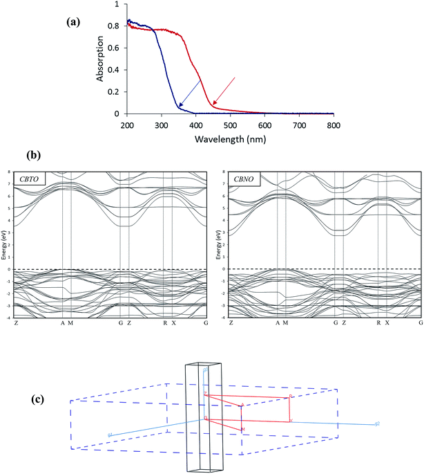 |
| | Fig. 2 (a) Experimental UV-vis absorption spectra of CBTO (blue) and CBNO (red). The cut-off wavelength positions are shown by arrows. (b) The calculated band structures of CBTO and CBNO. The Fermi energy (EF) is set to be 0 eV and is marked by a horizontal dashed line. (c) The first Brillouin zone of CBTO and CBNO in the reciprocal lattice. The red line corresponds to the path of the band structure diagram, and g1, g2, and g3 denote the reciprocal vectors. | |
The measured UV-vis absorption cut-off wavelengths for CBTO and CBNO samples are about 350 nm (3.54 eV) and 450 nm (2.74 eV), respectively.
The calculated band structures of CBTO and CBNO along the high symmetry directions in the first Brillouin zone are shown in Fig. 2b.
The Fermi energy level, EF, is chosen to be located at the position of 0 eV. The coordinates of the special points of the Brillouin zone (Fig. 2c) in terms of unit vectors of the reciprocal lattice are G (0, 0, 0), Z (0, 0, 0.5), R (0, 0.5, 0.5), X (0, 0.5, 0), A (0.5, 0.5, 0.5), and M (0.5, 0.5, 0). For CBTO and CBNO, the uncorrected band gap energies are 1.42 and 1.49 eV, respectively, which are smaller than the experimentally obtained band gap energies. Therefore, the underestimated band gaps were corrected by applying scissors operators 2.12 and 1.25 eV for CBTO and CBNO, respectively. As shown in Fig. 2b, for CBTO and CBNO, the valence band maximum (VBM) and conduction band minimum (CBM) are located at different points of the Brillouin zone, indicating that these compounds are indirect band gap semiconductors. The second derivative of band dispersion band-edge energy as a function of the wave vector k is related to the inverse of effective mass of electron or hole at the band extremes. For tetragonal crystals, the effective masses of either the hole or electron in the [100], [010] directions are equal.18 As can be seen from the graphical view of band structures, the valence and conduction bands in the [0 0 1] direction are almost flat and less dispersive compared to the [0 1 0] and [1 0 0]. The higher dispersive characteristics of the conduction and valence bands along the [0 1 0] and [1 0 0] directions indicate the low effective masses of electrons and holes in the CBTO and CBNO with respect to the [0 0 1] direction. On the other hand, the recombination of photo-generated charge carriers along the [0 0 1] direction in the CBTO and CBNO semiconductors with indirect band gaps are inefficient.
In order to analyze the composition of the electronic band structures, the corresponding total, site- and l-projected density of states (DOS) diagrams and their projected electronic wave functions (PEWF) are shown in Fig. 3–6. It is exigent to mention that the plane wave basis set and ultrasoft pseudo-potential present only the wave functions of the valence electron of atoms. The total DOS diagrams and their PEWFs in the (1 0 0) plane for CBTO and CBNO are presented in Fig. 3a and b to illustrate the interactions of O–M and O–Ba.
 |
| | Fig. 3 (a) Total density of states for CBTO (red) and CBNO (blue). The Fermi energy (EF) is set to be 0 eV. (b) Total charge density distribution for CBTO and CBNO in the (1 0 0) plane in order to illustrate the M–O and Ba–O bonds. | |
 |
| | Fig. 4 Site and angular projected density of states for CBTO (a) and CBNO (b). Red, green, and blue lines represent s, p, and d orbitals, respectively. The Fermi energy (EF) is set to be 0 eV. | |
 |
| | Fig. 5 Projected wave function contour plots for CBTO at six different energy ranges in the (1 0 0) plane illustrating the M–O and Ba–O bonds. | |
 |
| | Fig. 6 Projected wave function contour plots for CBNO at six different energy ranges in the (1 0 0) plane illustrating the M–O and Ba–O bonds. | |
It can be seen that the charge density contours for O and Ba atoms in the (1 0 0) plane containing O, Ba, and Cs atoms are spherical, suggesting a highly ionic bonding nature for O–Ba. On the other hand, the charge density contours in the (1 0 0) plane containing O and M atoms corroborate that there are highly ionic and highly covalent characters between O and M atoms in different O–M interactions. The analysis of PEWF indicates that the bonding nature in CBTO and CBNO is ionic and covalent. The total DOS can be projected into its partial components with respect to different atoms by solving the eigenvalues and eigenvectors in the Brillouin zone.19 The site- and l-projected DOS diagrams together with their PEWFs for conduction band minimum and five parts of valence band are shown in Fig. 4–6. For both systems, the quality of PDOS results is similar. The lowest-lying state from −20 to −18 eV (E1 region) is mainly due to Cs-5s and Cs-6s states. The second region in a higher energy range (E2 region) from −18 to −15 eV is essentially contributed by O-2s states with a minor admixture of Ba-5p and Ta-5s/6s/5p/5d states for CBTO or Nb-4s/5s/4p/4d states for CBNO. The PEWF of this region shows a weak hybridization between O atom and Ba, Ta or Nb atoms forming an ionic bonding. The next region (E3 region) from −11 to −9 eV mainly comes from Ba-5p states with a small contribution of O-2s states. The PDOS and PEWF of this region show weak s–p hybridization between O and Ba atoms forming an ionic bonding. The E4 region is predominantly composed of Cs-5p which is slightly hybridized with O-2p. The role of Ta or Nb electronic states in this energy region is very minor. At the top of valence band (E5 region), O-2p is overlapped with Ta-5d or Nb-4d, indicating p–d hybridization between O and Ta or Nb atoms forming a covalent bonding. The conduction band region (E6 region) is mainly from O-2p and Ta-5d or Nb-4d states. Since the valence and conduction bands (E5 and E6 regions) are mainly composed of O and Ta or Nb orbitals, the band gap excitation can occur at the MO6 units; consequently, the presence of a dipole at the MO6 units will play a significant role in separating of electrons and holes.
The optical property of a system is related to the transverse dielectric function ε(q,ω), where q is the momentum transfer in the photon–electron interaction and ω is the angular frequency for excitation. When the momentum transfer from the initial state to the final state is neglected, the complex dielectric function can be defined by the following mathematical relation:20
| | |
ε(ω) = ε1(ω) + iε2(ω)
| (3) |
The imaginary part of the complex dielectric function is related to the interband and intraband optical transitions between the different special k points at the first irreducible Brillouin zone. The intraband transitions are only important for metals; therefore, only direct and indirect interband transitions can be considered for semiconductors.21,22 ε2(ω) can be calculated from direct numerical evaluations of the momentum matrix elements of the electric dipole operator between the conduction and valence band wave functions:23,24
| |
 | (4) |
where
u is the polarization vector of the incident electric field,
r is the electron’s radius vector, and
e is electric charge,
ψck and
ψvk are the conduction and valence band wave functions at
k, respectively, and
ε0 is the vacuum permittivity. The summation of the equation is applied over all states from the occupied and empty bands, with their wave functions obtained in a numerical form after the optimization of the crystal structure. The real part,
ε1(
ω), of the dielectric function can be obtained from the imaginary part by using the Kramers–Krönig dispersion equation:
24,25| |
 | (5) |
where
P is the Cauchy principal value of the integral.
All optical properties were calculated with calculation geometry polycrystalline, instrumental smearing 0.5 eV. The vertical rigid shift of conduction band states (scissors operators) 2.12 and 1.25 eV was applied for CBTO and CBNO, respectively, due to underestimation of excitation energies with the DFT calculations. Fig. 7a shows the calculated average imaginary and real parts of the dielectric constants of CBTO and CBNO. The real part of the dielectric function at zero frequency shows that the static dielectric constants for CBTO and CBNO are 2.856 and 2.904, respectively. The square root of static dielectric constant gives an estimation of the refractive index of CBTO and CBNO, which are 1.69 and 1.70, respectively. The negative values of the real part of dielectric function are due to damping of the electromagnetic wave, and zero values indicate that longitudinally polarized waves are possible.20 The imaginary part of the dielectric function starts at 3.86 and 3.18 eV for CBTO and CBNO, respectively. Since the direct interband transitions have a significant contribution to the ε2(ω) with respect to indirect interband transitions, the maximum of the main peak for CBTO and CBNO belongs to A → A and M → M direct transitions. The main portion of the mentioned peaks for CBTO and CBNO is due to O-2p → Ta-5d and O-2p → Nb-4d interband transitions, respectively, whereas Ta-5d → O-2p and Nb-4d → O-2p interband transitions have smaller portion. In the electromagnetic radiation, electric and magnetic fields oscillate perpendicular to each other and perpendicular to the wave propagation. Interband and intraband transitions are resulted from the effect of electric field of photon on the complex dielectric function.26
 |
| | Fig. 7 (a) Real (solid line) and imaginary (dashed line) parts of the dielectric function of CBTO (red line) and CBNO (blue line). (b) Energy loss functions of CBTO (red line) and CBNO (blue line) as a function of photon energy. (c) Absorption spectra of CBTO (red line) and CBNO (blue line) as a function of photon energy. | |
When electrons pass through a homogeneous material, some electrons undergo inelastic scattering which means that they lose energy, also their paths slightly and randomly deflect. The energy loss function (ELF) is related to the dielectric function, as follows:27
| |
 | (6) |
Fig. 7b shows the energy loss function of CBTO and CBNO. The prominent peaks of ELF are located at 13.16 and 12.07 eV for CBTO and CBNO, respectively, where electrons are originally unbound to their lattice sites and start plasma oscillation. The collective oscillation of free electron gas density is a plasmon, and the corresponding energy is so-called plasmon energy (Ep). The values of plasmon energies are located in the ultraviolet (UV) region.
The quantity and nature of the optical band gap can be calculated using the conventional Tauc method from the optical absorption spectra. The absorption coefficient α(E) indicates the fraction of absorbed light when it passes through the material, and is written as:24
| |
 | (7) |
where
c is the velocity of light. Two types of optical transitions, direct and indirect, can be investigated by the following relation expression that was proposed by Tauc:
28| | |
α(E)E = A(E − Edirectg)0.5 + B(E − Eindirectg ± Ephonon)2
| (8) |
where
A and
B are fitting parameters,
Edirectg and
Eindirectg are direct and indirect optical gaps,
Ephonon is the phonon energy and
E is incident photon energy. The straight line segment in (
αE)
2 indicates a direct optical band gap, whereas the straight line segment in (
αE)
0.5 indicates an indirect optical band gap.
The calculated optical absorption curves in Fig. 7c show that the CBTO and CBNO are poor absorbers of visible light, or in other words, are ultraviolet (UV) light-responsive photocatalysts. Based on ISO standard ISO-21348,29 the main absorption of incident photons for CBTO and CBNO occurs at the vacuum ultraviolet region. Extrapolation of the linear portion of Tauc plots (Fig. 8) with the abscissa clearly indicates that CBTO and CBNO are indirect semiconductors so that optical and electronic gaps coincide. The indirect optical gap values indicate that CBTO and CBNO can absorb near UV light and violet light in the visible region, respectively.
 |
| | Fig. 8 Tauc plots of (a) CBTO and (b) CBNO. (αE)0.5 for indirect gap (blue line) and (αE)2 for direct gap (red line). | |
The positions of valence and conduction bands of a semiconductor and the redox potentials of an adsorbate are important factors for the oxidation and reduction capabilities of the semiconductor to undergo photoinduced electron transfer to the adsorbed species on its surface. The suitable potential level of the acceptor species is thermodynamically required to be more positive than the conduction band potential of the semiconductor (ECB), while the potential level of the donor needs to be more negative than the valence band position of the semiconductor (EVB) in order to donate an electron to the vacant hole.30 The band edge positions of CBTO and CBNO were calculated using empirical formulas, as follows:24,29,31–35
| | |
EVB = χ − Ee + 0.5EOpticalg
| (9) |
| | |
ECB = EVB − EOpticalg
| (10) |
where
Ee is the energy of free electrons on the hydrogen scale (approximately 4.50 eV) and
χ is electronegativity of a semiconductor, which is the geometric mean of the electronegativities of the isolated component atoms and is expressed, as follows:
36| |
 | (11) |
where
P is the number of atoms in the semiconductor and
k = 1, 2, 3, …,
P. The values of electronegativity of CBTO and CBNO are 5.40 and 5.37 eV, respectively, which were calculated from the experimental values of electronegativity (
i.e., Ba = 2.40 eV, Cs = 2.18 eV, Ta = 4.11 eV, Nb = 4.00, and O = 7.54 eV).
37 The relative dispositions of VB and CB edge potentials of CBTO and CBNO with respect to vacuum scale and NHE (normal hydrogen electrode) are displayed in
Fig. 9.
 |
| | Fig. 9 Relative dispositions of VB and CB potentials of CBTO and CBNO with respect to vacuum scale and NHE. | |
From the viewpoint of positions of VB and CB edge potentials, CBTO and CBNO are suitable photocatalysts without the need for co-catalysts. The VB potentials of CBTO and CBNO are more positive than the oxidation potential of O2/H2O (1.23 V), H2O2/H2O (1.77 V), and O3/H2O (2.07 V). Therefore, the photogenerated holes can oxidize H2O to produce active species O2, H2O2, and O3. These active species can further oxidize/decompose organic pollutants and dye molecules. The CB potential of CBTO is more negative than the redox potential of H2O/OH˙ (−0.83 V); therefore, the photogenerated electrons can produce H2 and active species O2˙− and OH˙, while the photogenerated electrons in CBNO can produce H2 and O2˙−. In addition to O2˙− and OH˙, which are active species to decompose organic pollutants, CBTO and CBNO are good candidates for photocatalytic hydrogen generation from water splitting.
4. Conclusions
The electronic, optical, and photocatalytic properties of the three-layer perovskite Dion–Jacobson phase CsBa2M3O10 (M = Ta, Nb) have been studied with the plane wave pseudo-potential using the density functional theory (DFT) method considering the exchange-correlation function within the generalized gradient approximation (GGA) proposed by Perdew, Burke, and Ernzerhof (PBE), as implemented in the CASTEP code. The structural study showed that the symmetry of the MO6 octahedra in CsBa2Ta3O10 and CsBa2Nb3O10 is reduced from the Oh point group to the centrosymmetric (D4h) and non-centrosymmetric (C4v) point groups, leading to special optical properties and photocatalytic activities. The population ionicity index indicated that there are different percentages of covalent nature in the M–O bonds, from pure covalent to pure ionic. The band structures and Tauc plots showed that CsBa2Ta3O10 and CsBa2Nb3O10 are ultraviolet (UV) light-responsive photocatalysts with an indirect band gap. The densities of state spectra and projected electronic wave functions were studied in detail to illustrate the origin of photocatalytic activity and the nature of M–O and Ba–O bonds. CsBa2Ta3O10 and CsBa2Nb3O10 with plasmon energies of 13.16 and 12.07 eV, respectively, were suggested to possibly oxidize/decompose organic pollutants and generate hydrogen from water splitting under UV light.
Notes and references
- V. Thangadurai, P. Schmid-Beurmann and W. Weppner, J. Solid State Chem., 2001, 158, 279–289 CrossRef CAS
 .
. - J. Gopalakrishnan and V. Bhat, Inorg. Chem., 1987, 26, 4299–4301 CrossRef CAS .
- M. Richard, L. Brohan and M. Tournoux, J. Solid State Chem., 1994, 112, 345–354 CrossRef CAS .
- M. Dion, M. Ganne and M. Tournoux, Mater. Res. Bull., 1981, 16, 1429–1435 CrossRef CAS .
- S. H. Byeon and K. Park, J. Solid State Chem., 1996, 121, 430–436 CrossRef CAS .
- M. Hojamberdiev, M. F. Bekheet, E. Zahedi, H. Wagata, K. Yubuta, A. Gurlo, K. Domen and K. Teshima, Nanoscale Search PubMed , submitted.
- S. J. Clark, M. D. Segall, C. J. Pickard, P. J. Hasnip, M. J. Probert, K. Refson and M. C. Payne, Z. Kristallogr., 2005, 220, 567–570 CAS .
- J. P. Perdew, K. Burke and M. Ernzerhof, Phys. Rev. Lett., 1996, 77, 3865–3868 CrossRef CAS .
- D. Vanderbilt, Phys. Rev. B: Condens. Matter, 1990, 41, 7892–7895 CrossRef .
- J. D. Pack and H. J. Monkhorst, Phys. Rev. B: Solid State, 1977, 16, 1748–1749 CrossRef .
- B. G. Pfrommer, M. Cote, S. G. Louie and M. L. Cohen, J. Comput. Phys., 1997, 131, 133–140 CrossRef .
- Z. Zhao, Z. Li and Z. Zou, Phys. Chem. Chem. Phys., 2011, 13, 4746–4753 RSC .
- J. Sato, H. Kobayashi and Y. Inoue, J. Phys. Chem. B, 2003, 107, 7970–7975 CrossRef CAS .
- J. He, E. Wu, H. Wang, R. Liu and Y. Tian, Phys. Rev. Lett., 2005, 94, 015504 CrossRef .
- S. Goumri-Said, H. Ozisik, E. Deligoz and M. Benali-Kanoun, Semicond. Sci. Technol., 2013, 28, 085005 CrossRef .
- M. K. Y. Chan and G. Ceder, Phys. Rev. Lett., 2010, 105, 196403 CrossRef CAS .
- J. Yu, Q. Xiang and M. Zhou, Appl. Catal., B, 2009, 90, 595–602 CrossRef CAS PubMed .
- J. Feng and B. Xiao, J. Phys. Chem. Lett., 2014, 5, 1278–1282 CrossRef CAS PubMed .
- S. Goumri-Said, H. Ozisik, E. Deligoz and M. B. Kanoun, Semicond. Sci. Technol., 2013, 28, 085005 CrossRef .
- C. Y. Yang and R. Zhang, Chin. Phys. B, 2014, 23, 026301 CrossRef .
- J. Feng, B. Xiao, J. C. Chen and C. T. Zhou, Solid State Sci., 2009, 11, 259–264 CrossRef CAS PubMed .
- T. Mahmood, C. Cao, F. K. Butt, H. Jin, Z. Usman, W. S. Khan, Z. Ali, M. Tahir, F. Idrees and M. Ahmed, Phys. B, 2012, 407, 4495–4501 CrossRef CAS PubMed .
- M. G. Brik, J. Phys.: Condens. Matter, 2013, 25, 345802 CrossRef CAS PubMed .
- E. Zahedi, Superlattices Microstruct., 2015, 81, 49–63 CrossRef CAS PubMed .
- R. Paschotta, Encyclopedia of Laser Physics and Technology, Wiley-VCH, New York, 1st edn, 2008 Search PubMed .
- S. K. Tripathy and V. Kumar, Mater. Sci. Eng., B, 2014, 182, 52–58 CrossRef CAS PubMed .
- T. Mahmood, C. Cao, W. S. Khan, Z. Usman, F. K. Butt and S. Hussain, Phys. B, 2012, 407, 958–965 CrossRef CAS PubMed .
- M. Meinert and G. Reiss, J. Phys.: Condens. Matter, 2014, 26, 115503 CrossRef PubMed .
- J. Liu, S. Chen, Q. Liu, Y. Zhu and Y. Lu, Comput. Mater. Sci., 2014, 91, 159–164 CrossRef CAS PubMed .
- A. L. Linsebigler, G. Lu and J. T. Yates, Chem. Rev., 1995, 95, 735–758 CrossRef CAS .
- H. Chen, L. Ding, W. Sun, Q. Jiang, J. Hu and J. Li, RSC Adv., 2015, 5, 56401–56409 RSC .
- S. Zhong, F. Zhang, W. Lu, T. Wang and L. Qu, RSC Adv., 2015, 5, 68646–68654 RSC .
- G. Zhang, W. Zhang, J. C. Crittenden, Y. Chen, D. Minakata and P. Wang, Chin. J. Catal., 2013, 34, 1926–1935 CrossRef CAS .
- Q. Zhang, H. Wang, S. Hu, G. Lu, J. Bai, X. Kang, D. Liuab and J. Gui, RSC Adv., 2015, 5, 42736–42743 RSC .
- Z. Zhao, J. Tian, D. Wang, X. Kang, Y. Sang, H. Liu, J. Wang, S. Chen, R. I. Boughton and H. Jiang, J. Mater. Chem., 2012, 22, 23395–23403 RSC .
- A. Chakraborty, R. Das and P. K. Chattaraj, Computational and Experimental Chemistry: Developments and Applications, Apple Academic Press, Inc, Canada, 2013 Search PubMed .
- R. G. Pearson, Inorg. Chem., 1988, 27, 734–740 CrossRef CAS .
|
| This journal is © The Royal Society of Chemistry 2015 |
Click here to see how this site uses Cookies. View our privacy policy here. 


