DOI:
10.1039/C5RA13425K
(Communication)
RSC Adv., 2015,
5, 82121-82126
Piezoresistive effect of p-type silicon nanowires fabricated by a top-down process using FIB implantation and wet etching
Received
9th July 2015
, Accepted 21st September 2015
First published on 22nd September 2015
Abstract
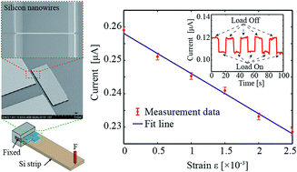
The piezoresistive effect in silicon nanowires (SiNWs) has attracted a great deal of interest for NEMS devices. Most of the piezoresistive SiNWs reported in the literature were fabricated using the bottom up method or top down processes such as electron beam lithography (EBL). Focused ion beam (FIB), on the other hand, is more compatible with CMOS integration than the bottom up method, and is simpler and more capable of fabricating very narrow Si nanostructures compared to EBL and photolithography. Taking the advantages of FIB, this paper presents for the first time the piezoresistive effect of p-type SiNWs fabricated using focused ion beam implantation and wet etching. The SiNWs were locally amorphized by Ga+ ion implantation, selectively wet-etched, and thermally annealed at 700 °C. A relatively large gauge factor of approximately 47 was found in the annealed SiNWs, indicating the potential of using the piezoresistive effect in top-down fabricated SiNWs for developing NEMS sensors.
Discovered by Smith in 1954, the piezoresistive effect in semiconductors has been investigated and employed in various micro electromechanical systems (MEMS) applications.1–6 Thanks to its availability, advanced MEMS fabrication process, and large gauge factor, silicon (Si) is among the first choice materials for developing piezoresistive transducers. The piezoresistive effect of bulk silicon has been utilized in AFM (atomic force microscope) cantilevers,7 acceleration, tactile, and pressure sensors.8–10
Recent research has paid a great attention to the piezoresistive effect of silicon nano structures, such as nanowires and nanosheets, to elucidate the quantum confinement effect in enhancement of the stress/strain sensing property for highly sensitive and miniaturized sensing devices.11,12 The giant piezoresistive effect in Si nanowires (SiNWs) with a gauge factor of up to 5000 reported by He and Yang has been a great motivation for a large number of studies on the characterization of the nanoscale effect in piezoresistance.13,14 Lugstein et al. reported the piezoresistive effect of ultra-strained SiNWs grown by the vapor–liquid–solid method, with a gauge factor comparable to that of bulk Si.15 Zhang et al. characterized the influence of strain on electrical conductance of SiNWs grown by a bottom up method, and reported a gauge factor of 67.1.16 The piezoresistance of SiNWs reported in the literature shows different gauge factor values, varying between several tens to several thousands.17–20 This large deviation of the gauge factors indicates that the piezoresistive effect in Si nanowires significantly depends on the surface state, concentration (e.g. depleted and highly doped Si), and the fabrication process of Si nanostructures. Additionally, the controversy regarding the existence of the giant piezoresistive effect in Si nanowires implies that more studies need to be carried out to better understand this effect in nanoscale Si.11
As well as the work on bottom-up grown Si, several studies have been carried out on the top-down fabricated SiNWs. Compared to the bottom-up process, the top-down process is more compatible with the conventional MEMS fabrication and CMOS integration. In most of the previous studies, SiNWs were fabricated using the electron beam lithography (EBL) or photolithography process in which a photoresist layer exposured to electron-beams or ultraviolet-light was employed as the etching mask to form SiNWs underneath.18,20,21 In comparison to these processes, focused ion beam (FIB) is simpler and has become increasingly popular in the fabrication of Si nanostructures.23 Additionally, FIB could also be utilized in device modifications because it can be used before, after or as a step in any lithography process.24 Furthermore, the thickness of SiNWs fabricated by FIB can also be accurately controlled by the penetration depth of the implanted ion, while the other top down processes (e.g. EBL, photolithography) require additional time-consuming steps such as wet/dry etching Si or thermal oxidation.25
To the best of our knowledge, to date, there has been no report on the characterization of the piezoresistive effect of SiNWs fabricated by localized amorphization through FIB implantation, selective wet etching, and re-crystallization by thermal annealing process. As the properties of SiNWs are changed due to amorphization and post-FIB thermal treatment,26 the piezoresistive effect of Si NWs fabricated using this process is expected to be different from that of bulk single crystalline Si. In this paper, we report on the piezoresistive effect in released SiNWs fabricated by a top-down process using the focused ion beam (FIB) method followed by wet etching of Si and thermal annealing. A relatively large gauge factor found in this top-down fabricated SiNWs indicates its high potential for nano electro mechanical systems (NEMS).
The SiNWs were fabricated from a silicon-on-insulator (SOI) wafer with the thicknesses of the device layer (low-doped n-type Si with a carrier concentration below 1014 cm−3), the insulation layer and the substrate layer being 2 μm, 0.2 μm and 200 μm, respectively. In the first step, the SOI wafer was diced into smaller strips with a dimension of 200 μm × 3 mm × 20 mm for the bending experiment. Next, an amorphous Si nanowires embedded in the top of the SOI wafer was formed using gallium ions (Ga+) implantation (FIB, ™Hitachi FB2200) at a dose of approximately 7 × 10¹⁵ ions per cm2. Since the etching rate of amorphous Si is much lower than that of single crystalline Si, the amorphous SiNWs were then formed after under-etching the crystalline Si layer underneath using wet etching with TMAH (tetramethylammonium hydroxide) as the etchant. Two electrode pads with a dimension of 200 μm × 200 μm were also formed for the electrical measurement. Finally, the amorphous SiNWs were thermally annealed at a high temperature of 700 °C for 60 minutes in a high vacuum chamber. Fig. 1 shows the scanning electron microscope (SEM) images of the fabricated SiNWs with their length of 10 μm, thickness of 60 nm and widths of 200 and 300 nm.
 |
| | Fig. 1 (a) Fabrication process using FIB Ga+ implantation and wet etching. (b) SEM images of SiNWs. | |
The amorphization by ion implantation and the recrystallization by thermal annealing of Si were confirmed using optical measurements. Fig. 2(a) shows the cross-sectional high resolution transmission electron microscopy (HRTEM) image of the Ga+ implanted Si films, illustrating the amorphized Si layer and the single crystalline Si layer underneath. After being annealed at 700 °C for 1 hour, the amorphized Si layer was recrystallized and poly crystalline Si was observed under HRTEM, Fig. 2(b). The grain size of the recrystallized Si layer was estimated based on the HRTEM image using an image processing technique.27 Accordingly, the annealed poly-silicon has grain sizes of several tens of nanometers. The mechanism of the amorphization can be explained due to the fact that, during the implantation process, Ga+ ion impact can knock Si atoms from the lattice, resulting in damage in the implanted region of the crystal. If the dose is high enough, the implanted layer will become amorphous. Meanwhile, in the thermal annealing process, silicon atoms can move into lattice sites and impurity (Ga+) can enter substitutional sites in the lattice.28 We also performed selected area electron diffraction (SAED) measurement of the amorphized and annealed Si films at the points marked inside the blue circles of Fig. 2(a) and (b). Based on the SAED data, the diffuse rings indicate that the ion implanted Si was amorphized (Fig. 2(c)), while the small spots making up a ring from the SEAD of the annealed Si indicate poly crystalline structures, Fig. 2(d). Another well-known technique used to investigate the crystallinity of materials is the Raman spectroscopy. The Raman spectrum was measured using a laser source with a spot size of 1 μm, on a released Si frame with a size of approximately 5 μm × 5 μm to avoid the influence of the Si substrate, as shown in the inset of Fig. 2(e). In the amorphous Si, no Raman peak was observed, while the Raman spectrum of the annealed Si shows a sharp peak at a wave number of approximately 520 cm−1, showing the evidence of the recrystallization due to thermal treatment, Fig. 2(e). The intensity of the Raman peak at 520 cm−1 of the annealed Si is smaller than that of pure Si films, indicating that thermal annealing did not fully recover the amorphized Si layer.29 Therefore, the above-mentioned optical measurements show strong evidence of the amorphization and recrystallization in our process.
 |
| | Fig. 2 (a and b) HRTEM images of ion implanted, and thermally annealed Si, respectively; (c and d) SAED measurements of the implanted and thermally annealed Si films, respectively. Note that the SEAD data was obtained at the points marked inside the blue circles of figure (a and b); (e) Raman spectroscopy of the original Si film, implanted Si and annealed Si. Note that to reduce the influence of the substrate, the Raman scattering measurements (™Renishaw inVia Raman microscope 514 nm) were performed on the released Si frames formed by under-etching the Si substrate as shown in the inset. The laser power in all experiments was 159 μW. | |
The concentration of impurity (Ga+) was characterized using the energy dispersive X-ray spectroscopy (EDX). The results show that the concentration of Ga is proportional to the amount of dose. At the dose of ∼1015 cm−2 used to fabricate the SiNWs in this study, the concentration of Ga was found to be ∼2 wt%, corresponding to an atomic concentration of approximately 1020 cm−3, which is in agreement with results reported by others previously.30 The electrical characteristics of the fabricated SiNWs was then performed using a ™HP 4145B analyzer. Experimental data shows that the conductivity of the annealed SiNWs (σ ≈ 0.2 S cm−1) is at least one order of magnitude higher than that of non-annealed SiNWs (σ ≈ 0.01 S cm−1), as shown in Fig. 3. This result indicates that the amorphous SiNWs were recrystallized after the annealing process, and therefore, their carrier mobility and thus their electrical conductivity were enhanced. Additionally, the carrier concentration also increased due to the activation of Ga+ by the thermal treatment. The semiconductor type of SiNWs was investigated by applying the back gate voltage (Vg). Under a positive Vg, the conductance of SiNWs increased, while at a negative Vg, the conductance of SiNWs decreased. This result indicates that SiNWs is a p-type semiconductor,31 which is formed by the implantation of Ga+ ions into the Si film. The carrier concentration was calculated using the following equation:
| |  | (1) |
where
Np is the concentration of activated impurity (Ga
+);
ρ is the resistivity of the SiNWs;
μp (100 cm
2 V
−1 s
−1) is the mobility of Ga
+ implanted Si after annealing;
30 and
q is the elementary charge (1.602 × 10
19 C). As a result, the carrier concentration was found to be approximately 2 × 10
16 cm
−3, which was relatively small in comparison to the dopant concentration (10
20 cm
−3). This result is understandable, since FIB usually creates crystal defects in Si nanostructures, and subsequently carriers can be trapped at the grain boundaries of Si NWs after annealing.
30
 |
| | Fig. 3 Comparison of the conductance of annealed/non-annealed SiNWs. Inset: the current–voltage curve of the non-annealed SiNWs plotted in nA scale. | |
To investigate the piezoresistance of the annealed SiNWs, we applied the bending beam method to induce strain into the SiNWs (Fig. 4(a) inset). The Si beam with SiNWs on it was clamped at one end, while the other end was applied with different loads. As the distance from the SiNWs to the surface of the Si beam (less than 2 μm) is relatively small in comparison to the thickness of the Si beam (200 μm), we assume that the strain induced into the SiNWs is approximately equal to that of the top surface of the Si beam. Therefore, the applied strain was calculated using the following equation:32
| |  | (2) |
where
M is the bending moment,
t is the thickness of the Si beam,
E is the Young's modulus of Si in [110] orientation, and
Ii is the area moment of inertia, respectively. Accordingly, the strain induced into the SiNWs was calculated to be in a range of 0 to 2500 ppm.
Fig. 4(a) shows the current–voltage curve of two types of annealed SiNWs with diameters of 200 nm and 300 nm under an applied strain of 2500 ppm. The decrease in the current indicates that under an uniaxial tensile strain in [110] orientation, the electrical resistance of both types of the SiNWs increased.
Fig. 4(b) presents the relationship between the shift of the current at a constant applied voltage of 20 V under different strains varied from 0 to 2500 ppm, showing a good linear relationship between strain and the change of the current. It is also evident that the piezoresistive effect in the fabricated SiNWs has a good reproducibility after several bending cycles (
Fig. 4(b) inset).
 |
| | Fig. 4 Characterization of the piezoresistive effect of the annealed SiNWs. (a) The change of current–voltage characteristics of the SiNWs with the widths of 200 nm and 300 nm under an applied strain of 2500 ppm. Inset: the bending experiment setup; (b) the linear relationship between the current and applied strain of the 300 nm SiNW at a constant applied voltage of 20 V. Inset: the reproducibility of the current change in the 300 nm SiNW after several loading cycles at an applied strain of 2500 ppm and an applied voltage of 10 V. (c) A one dimensional model of the crystalline structure of SiNWs which contains crystalline grains and grain-boundaries. | |
The gauge factor of the annealed SiNWs was then calculated from the ratio of the relative resistance change (ΔR/R) and the applied strain (ε):
| |  | (3) |
where
I is the current of the SiNWs. Consequently, the gauge factor of the 300 nm was found to be approximately 47, and independent of the applied voltage. Additionally, the gauge factors of the 200 nm SiNWs (GF = 45) and the 300 nm SiNWs (GF = 45) did not show a significant difference. The gauge factor is presented by the change of the geometry and resistivity of the SiNWs:
2,11| | | GF = 1 + 2γ + (Δρ/ρ)/ε | (4) |
where
γ is the Poisson ratio of the SiNWs which varies between 0 and 0.5. The change of geometry (1 + 2
γ) is between 1 and 2, which is smaller than 5% of the total gauge factor; therefore, it is obvious that the piezoresistive effect in the annealed SiNWs is due to the change of their electrical resistivity ((Δ
ρ/
ρ)/
ε). There are various hypotheses developed to explain the piezoresistive effect in SiNWs. He and Yang, and Rowe hypothesized that the potential created at the surface of SiNWs could lead to a piezopinch phenomenon, resulting in a giant piezoresistive effect.
13,14,20,22 However, this electric potential is only significant for SiNWs with a sufficiently small diameter and with a low doping sample (
ρ ≈ 10 Ωcm), thus we consider this effect is negligible in our SiNWs.
20 Another possible explanation is the quantum confinement which changes the band energy structure of Si when its size is shrunk down to several nanometers.
33,34 However, again, for SiNWs with a smallest dimension above 60 nm, the influence of quantum confinement is considered to be irrelevant.
Through thermal annealing, amorphous SiNWs are recrystallized, forming poly crystalline SiNWs;30,35,36 therefore, we employ the model of the piezoresistance in poly crystalline materials37,38 to explain the piezoresistive effect in the annealed SiNWs, as shown in Fig. 4(c). Accordingly, the resistivity of SiNWs can be expressed by a crystal region and a potential barrier region contribution:37,38
| |  | (5) |
where
ρcrys and
ρb are crystalline Si and potential barrier resistivity, respectively, while
L and
WB are the average grain size and the width of the potential barrier. The conductivity of crystalline Si (
σcrys) and potential barrier (
σb) are given by:
38,41| |  | (6) |
here
k,
T,
VB are the Boltzmann constant, the absolute temperature, and the height of potential barrier;
τ,
p and
m are the relaxation time, the carrier concentration and the effective mass of holes, where the subscripts
h and
l refer to the heavy hole and light hole in the valence band. Under mechanical strain, the heavy hole and light hole bands are split and warped, leading to the redistribution of holes in these two bands following the fact that holes will fill lower energy levels. Consequently, the re-population of holes results in the change of the hole effective mass. It is obvious that, according to
eqn (6), the hole transfer and mass change phenomenons in the valence band cause the conductivity of both crystalline Si and potential barrier to change. Utilizing the deformation potential theory into
eqn (6), the gauge factors of low doped p-type crystalline Si and the potential barrier were numerically calculated to be approximately 160 and 21, respectively.
38,39 These numerical results are in solid agreement with the experimentally measured GFs of lightly doped single crystalline Si
1,2 and poly-silicon.
37,40 Additionally, based on the model shown in
eqn (6), the gauge factor of p-type poly-silicon with its grain sizes varying from several tens to hundreds of nanometers has been estimated to be from 30 to 45. Therefore, in our annealed SiNWs with the grain size of several tens of nanometers, the gauge factor of 47 indicates that the piezoresistance of the as-fabricated SiNWs can be explained based on the band modification of single crystalline Si and consequently the change of the thermionic/diffusion currents flowing through grain boundaries under mechanical strain. We also expect that increasing the annealing temperature could enlarge the grain size of poly-silicon and thus could increase its gauge factors. In fact, several studies reported in the literature have proved that thermally annealing the ion implanted Si films at approximately 1000 °C could almost recover their crystallinity, and as a consequent improving the piezoresistance.
36,42,43 As such, Barlian
et al. reported that B
+ implanted Si films annealed at above 1000 °C possessed gauge factors of 60% to 90% of crystalline Si.
43 However, Ga
+ ions which have been commonly deployed in FIB are heavier than B
+, causing more crystal damages due to nuclear scattering. Therefore, it is still a challenge to fully recover the Ga
+ implanted Si films, and more studies need to be carried out to optimize the annealing conditions.
Finally, we estimate the piezoresistive coefficient of the annealed SiNWs. The longitudinal piezoresistive coefficient of the SiNWs (πl) is:
| |  | (7) |
here,
χ is the stress induced to the SiNWs; and
E is Young's modulus of the annealed SiNWs. In most previous studies on the piezoresistive effect in SiNWs, the Young's modulus of the SiNWs were assumed to be equal to that of the bulk Si, and there has been no report on the direct measurement of the Young's modulus of SiNWs for calculating the piezoresistive coefficient.
13,15–17 As the fabricated SiNWs were amorphized and then thermally annealed, it is important to investigate the mechanical properties of SiNWs for estimating the piezoresistive coefficient. Therefore, we applied the following
in situ method to measure the Young's modulus of the SiNWs. Annealed SiNWs fabricated by the same process were transferred onto a micro electrostatic comb actuator and fixed by tungsten. The stress applied to the SiNWs was controlled by varying the applied voltage of the comb drive. The deformation of the SiNWs was
in situ monitored using SEM as shown in
Fig. 5 inset. The detailed description of this experimental setup can be found elsewhere.
44 From the relationship between the applied stress and strain (
Fig. 5), the Young's modulus of the annealed SiNWs was calculated to be approximately 170 GPa, which is larger than the Young's modulus of amorphized SiNWS, and almost the same as that of bulk single crystalline Si. This result is in agreement with the results obtained from TEM that, after the thermal treatment, the amorphized SiNWs were recrystallized, becoming poly crystalline Si. Consequently, the longitudinal piezoresistive coefficient of the SiNWs was found to be 28 × 10
−11 Pa
−1.
 |
| | Fig. 5 Characterization of the mechanical property of SiNWs. Inset: (a) the SEM image of the SiNWs with dimensions of 60 nm × 200 nm × 5 μm, fabricated using FIB, and then thermally annealed. Two clamping pads were also formed at the ends of SiNWs to ease the consequent transferring and clamping process.44 (b) The schematic sketch of the experimental setup, in which the SiNWs were transferred on to an electrostatic comb actuator, and then fixed by tungsten. | |
We also conducted tensile testing on the annealed SiNWs. The results show that in all SiNWs, a brittle fracture occurred within the elastic deformation region, and no yield point was observed. The fractured strength of annealed SiNWs was measured to be approximately 4 GPa, indicating that the SiNWs can withstand a large strain of above 2.4%, which is approximately ten times larger than that of the maximum strain applied to the SiNWs in the experiment for characterizing piezoresistive effect shown in Fig. 4.
In conclusion, we characterized for the first time the piezoresistive effect in p-type SiNWs fabricated by using the focused ion beam implantation and wet etching process. Gallium ion implantation was carried out to locally amorphize silicon for selective wet etching and for modifying the semiconductor type and doping concentration. After thermally annealing, the electrical conductivity of the SiNWs was enhanced by at least one order of magnitude. The annealed SiNWs possess a large gauge factor of 47. The compatibility of the FIB process with conventional MEMS fabrications, the advantages of FIB over other EBL/photolithography processes, and the large piezoresistance indicate that the SiNWs fabricated using the method presented in this study are a good candidate for nano electromechanical sensing applications.
Acknowledgements
This work was performed in part at the Queensland node of the Australian National Fabrication Facility, a company established under the National Collaborative Research Infrastructure Strategy to provide nano and micro-fabrication facilities for Australia's researchers.
References
- C. S. Smith, Phys. Rev., 1954, 94, 42 CrossRef CAS.
- A. A. Barlian, W. T. Park, J. R. Mallon Jr, A. J. Rastegar and B. L. Pruitt, Proc. IEEE, 2009, 97(3), 513–552 CrossRef CAS PubMed.
-
(a) H.-P. Phan, P. Tanner, D. V. Dao, L. Wang, N.-T. Nguyen, Y. Zhu and S. Dimitrijev, IEEE Electron Device Lett., 2014, 35(3), 399–401 CrossRef CAS;
(b) H.-P. Phan, D. V. Dao, P. Tanner, L. Wang, N.-T. Nguyen, Y. Zhu and S. Dimitrijev, Appl. Phys. Lett., 2014, 104, 111905 CrossRef PubMed.
-
(a) A. Qamar, H.-P. Phan, D. V. Dao, P. Tanner, T. Dinh, L. Wang and S. Dimitrijev, IEEE Electron Device Lett., 2015, 36(7), 708–710 CrossRef;
(b) H.-P. Phan, D. V. Dao, L. Wang, T. Dinh, N.-T. Nguyen, A. Qamar, P. Tanner, S. Dimitrijev and Y. Zhu, J. Mater. Chem. C, 2015, 3, 1172–1176 RSC.
- R. W. Shao and K. Zheng, RSC Adv., 2015, 5(43), 34447–34450 RSC.
- M. Kumar and H. Bhaskaran, Nano Lett., 2015, 15(4), 2562–2567 CrossRef CAS PubMed.
- M. Tortonese, R. C. Barrett and C. F. Quate, Appl. Phys. Lett., 1993, 62, 834 CrossRef CAS PubMed.
- R. Amarasinghe, D. V. Dao, T. Toriyama and S. Sugiyama, IEEE Int. Conf. Micro Electro Mech. Syst., 18th, 2005, 2005, 351–354 Search PubMed.
- H. Yousef, M. Boukallel and K. Althoefer, Sens. Actuators, A, 2011, 167(2), 171–187 CrossRef CAS PubMed.
- M. D. Nguyen, H.-P. Phan, K. Matsumoto and I. Shimoyama, IEEE Int. Conf. Micro Electro Mech. Syst., 26th, 2013, 617–620 Search PubMed.
- A. C. H. Rowe, J. Mater. Res., 2014, 29(6), 731–744 CrossRef CAS.
- D. V. Dao, K. Nakamura, T. T. Bui and S. Sugiyama, Adv. Nat. Sci.: Nanosci. Nanotechnol., 2010, 1(1), 013001 CrossRef.
- R. He and P. Yang, Nat. Nanotechnol., 2006, 1, 42 CrossRef CAS PubMed.
- A. C. H. Rowe, Nat. Nanotechnol., 2008, 3, 312 CrossRef PubMed.
- A. Lugstein, M. Steinmair, A. Steiger, H. Kosina and E. Bertagnolli, Nano Lett., 2010, 10, 3204 CrossRef CAS PubMed.
- Y. Zhang, X. Y. Liu, C. H. Ru, Y. L. Zhang, L. X. Dong and Y. Sun, J. Microelectromech. Syst., 2011, 20, 959 CrossRef CAS.
- J. S. Milne, A. C. H. Rowe, S. Arscott and C. Renner, Phys. Rev. Lett., 2010, 105, 226802 CrossRef CAS.
- T. K. Kang, Nanotechnology, 2012, 23, 475203 CrossRef PubMed.
- P. Neuzil, C. C. Wong and J. Reboud, Nano Lett., 2010, 10, 1248 CrossRef CAS PubMed.
- Y. Yang and X. Li, Nanotechnology, 2011, 22, 015501 CrossRef PubMed.
- S. Zhang, T. Wang, L. Lou, W. M. Tsang, R. Sawada, D.-L. Kwong and C. Lee, J. Microelectromech. Syst., 2014, 23(6), 1396–1407 CrossRef CAS.
- F. Rochette, M. Casse, M. Mouis, A. Haziot, T. Pioger, G. Ghibaudo and F. Boulanger, Solid-State Electron., 2009, 53, 392 CrossRef CAS PubMed.
- S. Reyntjens and R. A. Puers, J. Micromech. Microeng., 2001, 11, 287–300 CrossRef CAS.
-
L. A. Giannuzzi, Introduction to focused ion beams: instrumentation, theory, techniques and practice, Springer Science & Business Media, 2006 Search PubMed.
- A. A. Tseng, Small, 2005, 1(10), 924939 CrossRef PubMed.
- T. Fujii, T. Namazu, K. Sudoh, S. Sakakihara and S. Inoue, J. Eng. Mater. Technol., 2013, 135(4), 041002 CrossRef.
- M. K. Hatalis and D. W. Greve, J. Appl. Phys., 1988, 63(7), 2260–2266 CrossRef CAS PubMed.
-
R. C. Jaeger, Introduction to Microelectronic Fabrication: Volume 5 of Modular Series on Solid State Devices, Prentice Hall, New Jersey, 2nd edn, 2001 Search PubMed.
- A. A. Parr, K. Gill, D. J. Gardiner, J. D. Hoyland, D. Sands, K. Brunson and R. T. Carline, Semicond. Sci. Technol., 2002, 17(1), 47 CrossRef CAS.
- R. Bottger, L. Bischoff, B. Schmidt and M. Krause, J. Micromech. Microeng., 2011, 21, 095025 CrossRef.
- Y. Cui, X. Duan, J. Hu and C. M. Lieber, J. Phys. Chem. B, 2010, 104(22), 5213–5216 CrossRef.
-
(a) H.-P. Phan, D. V. Dao, P. Tanner, J. Han, N.-T. Nguyen, S. Dimitrijev, G. Walker, L. Wang and Y. Zhu, J. Mater. Chem. C, 2014, 2, 7176–7179 RSC;
(b) H.-P. Phan, A. Qamar, D. V. Dao, T. Dinh, L. Wang, J. Han, P. Tanner, S. Dimitrijev and N.-T. Nguyen, RSC Adv., 2015, 5(69), 56377–56381 RSC.
- T. Ivanov, T. Gotszalk, T. Sulzbach and I. Rangelow, Ultramicroscopy, 2013, 97, 77–84 Search PubMed.
-
K. Nakamura, D. V. Dao, Y. Isono, T. Toriyama and S. Sugiyama, Nanowires, Electronic States and Piezoresistivity in Silicon Nanowires, In-Tech, Vienna, Austria, 2010, ch. 15, pp. 297–314 Search PubMed.
- S. Saxena, IEICE Trans. Electron., 2010, 93(10), 1495–1498 CrossRef.
- Y. J. Xiao, F. Z. Fang, Z. W. Xu and X. T. Hu, Appl. Surf. Sci., 2015, 343, 56–69 CrossRef CAS PubMed.
-
X. Liu, C. Shi and R. Chuai, Solid State Circuits Technologies, 2010, ISBN: 978-953-307-045-2 Search PubMed.
- P. Kleimann, B. Semmache, M. le Berre and D. Barbier, Phys. Rev. B: Condens. Matter Mater. Phys., 1998, 57(15), 8966 CrossRef CAS.
- T. Toriyama and S. Sugiyama, J. Microelectromech. Syst., 2002, 11(5), 598–604 CrossRef CAS.
- D. Schubert, W. Jenschke, T. Uhlig and F. M. Schmidt, Sens. Actuators, 1987, 11(2), 145–155 CrossRef CAS.
- P. J. French and A. G. R. Evans, Piezoresistance in polysilicon and its applications to strain gauges, Solid-State Electron., 1989, 32(1), 1–10 CrossRef CAS.
-
J. C. Doll and B. L. Pruitt, Piezoresistor Design and Applications, Springer, 2013 Search PubMed.
- A. A. Barlian, S. J. Park, V. Mukundan and B. L. Pruitt, Sens. Actuators, A, 2007, 134(1), 77–87 CrossRef CAS PubMed.
- T. Fujii, K. Sudoh, S. Sakakihara, M. Naito, S. Inoue and T. Namazu, Jpn. J. Appl. Phys., 2013, 52(11R), 110118 CrossRef.
|
| This journal is © The Royal Society of Chemistry 2015 |
Click here to see how this site uses Cookies. View our privacy policy here.