
Electronic structure and ultrafast charge transfer dynamics of phosphorous doped graphene layers on a copper substrate: a combined spectroscopic study†
Dunieskys Gonzalez Larrudeab,
Yunier Garcia-Basabe*cd,
Fernando Lázaro Freire Juniorbe and
Maria Luiza M. Roccoc
aGraphene and Nano-materials Research Center – MackGraphe, Mackenzie Presbyterian University, 01302-907, São Paulo, SP, Brazil
bPhysics Department, Pontifícia Universidade Católica do Rio de Janeiro, 22451-900, Rio de Janeiro, RJ, Brazil
cInstitute of Chemistry, Federal University of Rio de Janeiro, Rio de Janeiro, 21941-909, Brazil. E-mail: yunier.basabe@unila.edu.br; Fax: +55-21-3938-7265; Tel: +55-45-3576-2113
dFederal University of Latin-American Integration, Foz do Iguaçu, 85866-000, PR, Brazil
eBrazilian Center for Physical Research, 22290-180, Rio de Janeiro, RJ, Brazil
First published on 24th August 2015
Abstract
Graphene sheet layers were grown by chemical vapor deposition (CVD) under a polycrystalline copper substrate using methane (CH4) and triphenylphosphine (P(C6H5)3) as carbon and phosphorous precursors, respectively. The films obtained from the CH4 and P(C6H5)3 chemical precursors were labeled as G/Cu and GP/Cu, respectively. Electronic structure investigation was performed on these two graphene samples combining different spectroscopic techniques. Raman spectroscopy shows the presence of single and multilayers in G/Cu and GP/Cu, respectively. A blue shift of 30 cm−1 of the 2D band in the GP/Cu film with respect to G/Cu is evidence of the p-type doping of GP/Cu. X-ray photoelectron and reflection electron energy loss spectroscopy (REELS) confirm the bilayer formation in the GP/Cu film. REELS also shows that the presence of phosphorous does not open the electronic band gap of the graphene film. The work function of 4.3 eV for G/Cu and 4.8 eV for GP/Cu films were determined by ultraviolet photoelectron spectroscopy. The increase of the work function is attributed to the electron transfer to the Cu substrate. The partially unoccupied densities of states in phosphorous doped graphene (GP/Cu) were evaluated by X-ray photoabsorption spectroscopy. The core-hole clock approach using resonant Auger spectroscopy was employed for investigating the charge transfer dynamics around the P K-edge in GP/Cu. Ultrafast charge transfer delocalization on a time scale of femtoseconds was observed, demonstrating a strong electronic coupling between unoccupied states of the phosphorous and the conduction band of the copper substrate. The combined spectroscopic results suggest p-type doping in GP/Cu by the electron transfer mechanism.
1. Introduction
Graphene, a monolayer of sp2 hybridized carbon atoms, has been attracting much interest because of the novel properties associated with its unique band structure,1,2 originating from its massless fermions due to the linear dispersion of energy bands near the Dirac points.3 Among the extraordinary properties such as an anomalous integer quantum Hall effect at room temperature, insensitivity to external electrostatic potentials, and extremely high mobility on the order of 1 × 105 cm2 V−1 s−1,4 graphene is expected to become one of the most promising materials for electronic devices. However, graphene is a semimetal with zero band gap at the Dirac point, which restricts its applications as a semiconductor material. Therefore, opening a sizeable and tunable band gap in graphene via different functionalization paths is a significant challenge for graphene application. The substitutional doping of graphene with heteroatoms, such as nitrogen (N), boron (B) and phosphorus (P) has been investigated experimentally and theoretically.5–11 Nevertheless, experimental research on phosphorous doped graphene (GP) is very scarce when compared to N and B, and only few reports have been published.12–14 Cruz-Silva et al.15 found that phosphorous maintains sp3 hybridization and bonds to the carbon atoms with tetrahedral orbitals, inducing structural strain in the carbon lattice. The P dopant prefers to lie out of the graphene plane. Denis et al.16 demonstrated using Density Functional Theory (DFT) calculations that the doping of P atoms into the graphene lattice could open the largest band gap (0.67 eV spin up, 0.66 eV spin down) when compared with other heteroatoms doped graphene monolayer.Other important property observed is that the incorporation of P atoms into the carbon framework creates new active sites for the oxygen reduction reaction (ORR) and was demonstrated to be better than or at least comparable to that of the benchmark platinum/carbon catalyst.17 If gases, such as NO2, NO, SO2, are adsorbed onto P-graphene, the electronic conductivity of the GP will be changed.18 By monitoring the conductivity variation after the adsorption of molecules, the GP can also be used as a sensitive detector of these toxic gases. This means that the sensitivity of graphene based chemical gas sensors could be drastically improved by introducing the appropriate dopant or defect. Alternatively to substitutional doping, chemical doping, the charge transfer between graphene and adsorbates, would lead to p- or n-type by tuning the carrier concentrations in graphene. This apparently does not affect the mobility of either electrons nor holes and as a result the prospects of graphene-based electronics can be improved.19,20 Another important application of phosphorous doped graphene which has gained interest in the last years is related to its use as electrode in lithium- and sodium-ion batteries electrode.21–23
More recently Mastrapa, et al.14 have synthesized graphene layers by CVD using different masses of triphenylphosphine precursor. They report spectroscopic and microscopy investigation of graphene layer transferred to Si/SiO2 substrate using polymethylmethacrylate (PMMA). In this case they report from XPS characterization the formation of inhomogeneous films composed mainly by single-layer graphene, with small regions of few layers graphene, together with small nanostructures of oxidized phosphorous when 10 mg of the precursor was used. They also report that the use of larger amount of precursor, heavily damages the graphene layer through the increase of the number of small cluster of nanostructures, which are most likely due to clustering of P atoms on top of the graphene surface.
So, the study of the electronic structure of graphene phosphorous doped materials can be an important key for exploring new applications. Therefore, in this work graphene was grown using high vacuum Chemical Vapor Deposition (CVD) on polycrystalline Cu foils with two carbon precursors, methane (CH4) and triphenylphosphine (P(C6H5)3).14 Raman, Reflection Electron Energy Loss (REELS) and X-ray photoelectron (XPS) spectroscopies were employed to characterize the effect of the phosphorous doping in the graphene layer. The electronic structure of graphene layers was investigated by ultraviolet photoelectron spectroscopy (UPS) by determining the work function of pristine and phosphorous doped graphene. The P-1s X-ray photoabsorption (XAS) spectrum was used to analyze the partial density of unoccupied electronic states in phosphorous doped graphene (GP/Cu).
Besides, ultrafast charge transfer dynamics was studied using the core-hole clock (CHC) approach coupled with the Resonant Auger Spectroscopy (RAS) measured around the P K-edge. This approach is element-sensitive based on the study of the core-hole decay spectra measured while tuning the incoming photon energy across an atomic absorption edge. The decay spectra measured from RAS have different behavior if the excited electron is atomically localized during the core-hole lifetime or if the electron is transferred to the environment (i.e. substrate) before core-hole refilling. In the first case, two different final states can be reached: the spectator (2h1e; h = hole and e = electron) state, where the excited electron does not participate in the core-hole filling, and the participator (1h) state, where the excited electron is involved in the core-hole decay, both processes known as resonant contributions. The second case corresponds to a two holes (2h) final state, called normal Auger or non-resonant Auger contribution, similar to the decay following ionization. The charge transfer time (τCT) is calculated from the branching ratio of the resonant and non-resonant Auger decay channels and using the natural lifetime (τCH) of the core-excited state as an internal reference clock: τCT = (Iresonant/Inon-resonant) × τCH.24,25 The τCH values of low Z elements are in the femtosecond time scale, therefore very fast processes (from 10−15 s up to 10−18 s) can be achieved from the CHC approach. A schematic representation of the core-hole clock method is shown in Scheme 1.26
 | ||
| Scheme 1 Schematic representation of the core-hole clock method. (A) Core level resonant excitation into an unoccupied molecular orbital, LUMO. (B) Spectator decay process with a 2h1e final state. (C) Participator decay process, 1h final state. (D) The electron is transferred to the substrate (or molecular environment) and core-hole decay processes via a normal Auger decay with a 2h final state.26 | ||
The use of the core-hole clock approach to investigate charge transfer dynamics in graphene is very scarce. Lizzit et al.27 used CHC to investigate charge transfer dynamics in graphene monolayer with variable substrate coupling, using adsorbed argon.
2. Experimental
2.1 Materials
The graphene sheets were obtained in a high vacuum (low pressure) CVD system using methane (CH4), triphenylphosphine (P(C6H5)3) (Sigma-Aldrich 99.98%) and hydrogen gas as precursors on 25 μm thick copper foils (Sigma-Aldrich, 99.98%). More detailed deposition conditions were reported by Mastrapa et al.14 The copper foils were annealed up to 1000 °C under a 2 sccm H2 flux during 20 min. The maximum P(C6H5)3 vapor pressure inside the chamber was 40 mTorr for 20 mg of precursor and the growth time was about 30 min. As a control sample, graphene prepared from CH4 through a typical CVD process was used.282.2 Sample characterization
The quality and number of layers of the as-grown graphene films were evaluated by Raman spectroscopy using a confocal micro-Raman spectrometer (NT-MDT, NTEGRA SPECTRA) equipped with a 473 nm laser excitation source (power at sample is below 0.1 mW), a 100× objective and a CCD detector. The focused laser spot has a diameter of about 1–2 μm, and the spectral resolution is about 3 cm−1. The wavenumber calibration was achieved based on the standard values for crystalline silicon band checked at 520 cm−1 (ref. 29) and the vibrational stretching mode of atmospheric nitrogen30 at 2332 cm−1. All the spectra were recorded at room temperature and the peaks fitted using the Lorentz function in Origin software.X-ray Photoelectron Spectroscopy (XPS) and Reflection Electron Energy Loss Spectroscopy (REELS) spectra were carried out in a UHV ESCALAB 250Xi spectrometer, equipped with a hemispherical electron energy analyzer. XPS spectra were measured using monochromatized Al Kα (hν = 1486.6 eV) excitation energy and two different electron emission angles (0° and 50°) with respect to the surface normal. REELS spectra were measured using a primary electron beam energy Ep = 1000 eV, with spot size of 150 μm, an electron current of about 5 nA and constant analyzer pass energy of 12 eV. The full-width at half-maximum (FWHM) of the elastic peak in this experimental condition was 0.6 eV.
UPS spectra were measured in the same UHV chamber using HeI (21.2 eV) source of a helium discharge lamp with a pass energy 10 eV. UPS spectra were used for determining the effect of phosphorous doping in the work function (ϕ) of graphene materials. The ϕ values were determined by subtracting the high binding energy cutoff from the HeI excitation energy.31–33
Photoabsorption (XAS) spectra were measured at the soft X-ray spectroscopy (SXS) beamline at the Brazilian Synchrotron Light Source (LNLS). InSb(111) double-crystal monochromator was used to cover the phosphorus K-edge. XAS spectra were collected in the total electron yield mode (electron current at the sample) simultaneously with a photon flux monitor (Au grid). The final data was normalized by this flux spectrum to correct for fluctuations in beam intensity. The energy calibration at the InSb(111) double crystal monochromator was performed using the 1s → 3p transition of a silicon wafer.
Resonant Auger spectra (RAS) were also measured at the SXS beamline in the same ultrahigh vacuum chamber with a base pressure of 10−8 mbar using a hemispherical electron energy analyzer. The take-off direction of the Auger electrons was 45° and a pass energy of 20 eV was used during the experiment. The binding energy scale was calibrated using Au (4f7/2) signal. A linear combination of Gaussian (G) and Lorentzian (L) profile shape functions was used in the fitting of the spectra and the background correction was performed using a Shirley function. Possible surface charging effect (shift in electron energy) was monitored using the C 1s photoemission line located at binding energy of 285 eV.
3. Results and discussion
Raman spectra of the as-grown graphene films on copper foil using CH4 and triphenylphosphine as C and C/P sources, respectively, are shown in Fig. 1. The major Raman features of graphene are the so-called D band (∼1360 cm−1), G band (∼1580 cm−1) and 2D band (∼2720 cm−1). The D band (or doubly-resonant disorder-induced D mode) originates from the breathing modes of sp2 atoms in the ring, but to be active the ring must be adjacent to a graphene edge or a defect. The G band originates from in-plane vibration of sp2 carbon atoms and the 2D band from a two phonon double resonance Raman process. The 2D band is widely used to distinguish single-layer graphene from multi-layer graphene films while the strength of the D band is indicative of the degree of defects in the sample.34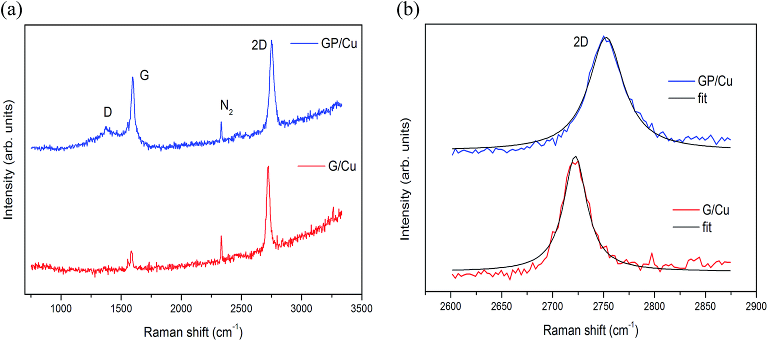 | ||
| Fig. 1 Raman spectra of (a) G/Cu and GP/Cu with the (b) 2D Lorentzian fits of the graphene sheets. | ||
The 2D line of pure G/Cu and doped GP/Cu located at 2722 and 2752 cm−1 are very well described by a single Lorentzian with a full-width at half-maximum (FWHM) of 27 and 39 cm−1, respectively, which agrees with the notion that the samples are covered mainly by monolayer graphene as can be seen in Fig. 1b. The Raman spectrum of the G/Cu is clearly different from the GP/Cu. First, the G (1594 cm−1) and 2D (2752 cm−1) bands are noticeably blue shifted by 9 cm−1 and 30 cm−1, respectively, as for hole doping, due to the charge transfer induced modification of the equilibrium lattice parameter.35 This result shows that most of the P atoms are not substitutional on the graphene framework. In case of substitutional P doping the 2D band must experience a redshift. The Raman spectrum of GP/Cu also shows high intensity of the D peak, indicating a rather high defect density of the basal plane. The intensity ratio ID/IG, between D and G bands, determined after background caused by fluorescence from the copper substrate was removed,36 increases from 0.09 in G/Cu to 0.29 in GP/Cu. Finally, the Raman spectrum of G/Cu shows a low sp3 amorphous carbon content,37 originating from clusters of hydrogenated amorphous carbon/aromatic clusters,38 possibly agglomerated on top of phosphorous residues due to the surface roughness of the copper foil used as catalytic substrate.
Fig. 2 shows XPS survey spectra of the graphene layer (G/Cu) and graphene doped with phosphorus (GP/Cu) on copper substrate. A strong contribution of the Cu substrate is observed from XPS spectra recorded at 0°. On the other hand, XPS spectra measured at 50° is more representative of graphene layers. The quantitative chemical analysis in each graphene film, obtained from these spectra, is resumed in Table 1. The atomic% of P element in GP/Cu graphene is very small compared to the Cu and C elements, and cannot be detected directly from the survey spectra. Therefore, the amount of P in the graphene film was determined from high resolution P 2p core level spectra and taking in consideration its atomic sensitivity factor.39 It is presented in Fig. SI1 in ESI.† The P atomic% value reported in Table 1 is relative to the carbon content.
 | ||
| Fig. 2 XPS survey spectra measured at electron emission angles of 0° (left) and 50° (right) of pure graphene and phosphorous doped graphene on Cu substrate. The electron emission angle is defined with respect to the surface normal. | ||
| Elements | G/Cu-0° | G/Cu-50° | GP/Cu-0° | GP/Cu-50° |
|---|---|---|---|---|
| O | 16.0 | 14.3 | 2.2 | 1.9 |
| C | 37.7 | 67.4 | 77.1 | 89.1 |
| Cu | 46.3 | 17.3 | 20.7 | 8.0 |
| P/C | 0 | 0 | — | 1.0 |
The fitting procedure of the high resolution C 1s spectra measured at 50° for G/Cu and GP/Cu is presented in Fig. 3. Three components were used for the deconvolution of the spectra, one at 284.3 eV attributed to C![[double bond, length as m-dash]](https://www.rsc.org/images/entities/char_e001.gif) C sp2 bonds, one at 285.4 eV attributed to C–C sp3 hybridization or carbon defect and another at 286.6 eV associated to C–OH.40–43 As reported previously by Kwon et al.43 for graphene doped with different metal chlorides, the doping effect in the C 1s core level occurs principally in the ICC/IC–C intensity ratio. We can observe from this quantitative analysis that ICC/IC–C ratio increases from 9.7 in G/Cu to 16.7 in GP/Cu film. According to Kwon et al.,43 the increased ICC/IC–C ratio can be associated with p-doping by electron transfer from sp3 hybridization to the metal becoming sp2. In our case, the electron transfer is occurring to the Cu substrate. The C–O percentage is also reduced in the phosphorous doped graphene. This result, together with the reduction of the oxygen atomic% obtained from the XPS survey spectrum at electron emission angle of 50° in G/Cu and in GP/Cu (see Table 1) suggests that oxygen species are underlying the graphene surface.
C sp2 bonds, one at 285.4 eV attributed to C–C sp3 hybridization or carbon defect and another at 286.6 eV associated to C–OH.40–43 As reported previously by Kwon et al.43 for graphene doped with different metal chlorides, the doping effect in the C 1s core level occurs principally in the ICC/IC–C intensity ratio. We can observe from this quantitative analysis that ICC/IC–C ratio increases from 9.7 in G/Cu to 16.7 in GP/Cu film. According to Kwon et al.,43 the increased ICC/IC–C ratio can be associated with p-doping by electron transfer from sp3 hybridization to the metal becoming sp2. In our case, the electron transfer is occurring to the Cu substrate. The C–O percentage is also reduced in the phosphorous doped graphene. This result, together with the reduction of the oxygen atomic% obtained from the XPS survey spectrum at electron emission angle of 50° in G/Cu and in GP/Cu (see Table 1) suggests that oxygen species are underlying the graphene surface.
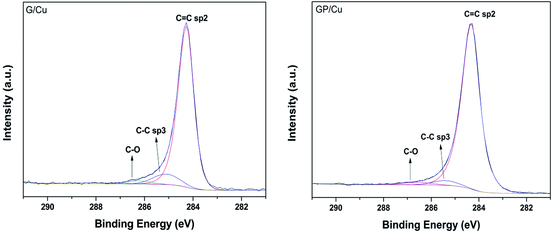 | ||
| Fig. 3 High resolution C1s XPS spectra of G/Cu (left) and GP/Cu (right) films. The three features CC sp2, C–C sp3 and C–O used in the fitting procedure are also shown. | ||
REELS spectra of G/Cu and GP/Cu are shown in Fig. 4. The spectra were normalized with respect to the elastic peak appearing at 0 eV. There are some distinguishable features within the REELS spectra. The inelastic loss peak at 6.2 eV in G/Cu spectra is related to π–π* excitation in aromatic carbon rings, while the broad band around 23 eV is originated by π + σ bulk plasmon loss. A blue shift to 6.7 eV in energy for π–π* excitation and 26.8 eV for π + σ plasmon loss is observed in phosphorous doped graphene layers (see GP/Cu spectra). This can be indicative of the existence of more than one single layer graphene regions,42,44 which is in agreement with XPS and Raman results. The shoulders around 14 and 19 eV appearing in the GP/Cu spectra are associated to σ–π* and π–σ* single electron transitions, respectively.45 The peak at 4.1 eV observed in GP/Cu REELS spectrum is also an evidence of the formation of an amorphous carbon layer,42 which is in agreement with Raman results. The peak located around 2.4 eV for G/Cu graphene layer is associated with the presence of hydrogen species46,47 due to the fact that a constant hydrogen flux was kept in the CVD deposition procedure. The weak signals appearing at 32.5 and 33.3 eV for G/Cu and GP/Cu, respectively, are associated with inter-band transitions.45 The electronic gap was determined following the procedure found in the literature.48–50 Similar electronic gaps of 1.64 and 1.63 eV were obtained for G/Cu and GP/Cu films, respectively. These values are higher than those reported for graphene single layer.51–54 The high electronic band gap found here may be due to strong interfacial interaction of the graphene layer with the Cu substrate.51,55 However, it is noteworthy that P doping doesn't induce a gap opening at the Dirac point of the two-dimensional electronic structure of graphene.
 | ||
| Fig. 4 REELS spectra of pure graphene (G/Cu) and phosphorous doped graphene (GP/Cu) on Cu substrate. The REELS spectrum of the Cu substrate is also shown. The graphs in the right show the low energy loss region used for determining the electronic gap. | ||
The effect of phosphorus doping graphene in the work function (ϕ) was analyzed by ultraviolet HeI photoemission spectra (UPS). Fig. 5 shows the secondary electron cutoff region of the Cu substrate, G/Cu and GP/Cu. The secondary electron cutoff was determined by extrapolating two dashed lines from the background and the onset in the secondary electron threshold. The ϕ of the Cu substrate and G/Cu were measured to be 4.7 and 4.3 eV, respectively, which are close to values reported in the literature.42,43,56 The Φ value obtained for GP/Cu was 4.8 eV, which is greater than that of G/Cu. This behavior is typical for p-doped graphene; however, n-type doping must be expected if interstitial or substitutional phosphorous doping occurs.5 Therefore, no substitutional phosphorous doping is observed and the increase of 0.5 eV in GP/Cu work function can be associated with electron transfer to the Cu substrate, shifting the Fermi level from the Dirac point to the valence band.
 | ||
| Fig. 5 UPS-HeI spectra covering the secondary electron threshold region for Cu substrate (a), G/Cu (b) and GP/Cu (c), respectively. The cutoff binding energies (Ecutoff) determined by the extrapolation procedure and the work function obtained by subtraction of ϕ = 21.2 − Ecutoff are also shown. | ||
Fig. 6 shows XAS spectrum following phosphorus K-edge photoexcitation for doped GP/Cu film. P K-edge XAS probes the excitation of electrons from P 1s to unoccupied p states in the LUMOs. Thus, the decay of the core-hole will generate holes in the valence band through the Auger mechanism. For the assignment of the XAS transitions theoretical calculations would be necessary. However, the assignment of these transitions can be suggested by considering P-1s XAS spectra of phosphorous organic compounds as the case of triphenylphosphine used as precursor.57,58 This spectrum is characterized by a strong and well defined peak at 2151.5 eV induced by transition from 1s state into orbitals with e symmetry mainly formed by phosphorus–carbon bond. The small shoulder at 2147.5 eV is due to 1s electron transition to a pπ*-orbital formed by the aromatic ligands in the higher coordination shells of the absorbing phosphorous with symmetry a1. The broad transition at 2157.5 is attributed to 1s–σ* (P–C) orbital. The numbered arrows represent the photon energies selected to collect the RAS data.
 | ||
| Fig. 6 P-1s XAS spectrum of GP/Cu film. The photon energies used for the measurement of the RAS spectra are marked as numbered arrows. | ||
Phosphorous-KL2,3L2,3 RAS spectra of GP/Cu film are presented in Fig. 7. RAS spectra are characterized by two features at different kinetic energies. The assignment of the features is based on previous report on solid phosphorous compounds.59,60 The peak at 1851.8 eV kinetic energy is associated with 1D2 normal Auger (labeled as CT) process due to the fact that its position (in kinetic energy scale) is almost constant with the increase of the incident photon energy and mainly because it is the only peak measured outside the P-1s resonance (hν = 2175 eV) as reported in Fig. SI2.† The normal Auger contribution is a strong evidence of charge delocalization in GP/Cu film. The other peak appearing at 1855 eV in the RAS spectrum measured at 2150.5 eV is attributed to a spectator Auger peak. A shift to higher kinetic energies with the increase of the incident photon energy is observed, as expected.
 | ||
| Fig. 7 P-KL2,3L2,3 RAS spectra measured at different photon energies labeled from 1 to 5 in Fig. 6. The graph in the left panel represents the full spectra measured from 1845 to 1870 eV in electron kinetic energy. The right part is a zoom representing CT (red) and spectator (blue) signals. | ||
Charge transfer times (τCT) for GP/Cu film was calculated taking into account the core-hole clock (CHC) approach,24,61 which uses the calculated areas for normal and spectator peaks obtained by the deconvolution procedure of the RAS spectra and phosphorous core-hole lifetime (τCH) of 1.25 fs (ref. 62) and the equation τCT = {I(spectator)/I(normal Auger)} × τCH. Table 2 presents the τCT calculated from the RAS spectra measured at different photon energies around P-1s absorption edge. Considering that the time scale determined from the CHC approach for P1s core level is limited within 0.125 ≤ τCT ≤ 12.5 fs,24,59 the value of 1.72 fs obtained on resonance (2151.5 eV) shows that fast charge delocalization is occurring in GP/Cu film. The τCT shortens with the increase of the excitation energy as observed in Table 2. This behavior may reflect strong overlap between more energetic unoccupied states of phosphorous and the Cu substrate conduction band, like was found for sulfur deposited on metallic substrates.63,64 The fast charge delocalization in GP/Cu is evidence that p-type doping is occurring by electron transfer from the graphene layer to the Cu substrate.
| Label | Photon energy (eV) | τCT (fs) |
|---|---|---|
| 1 | 2150.5 | 2.15 (5) |
| 2 | 2151.5 | 1.72 (3) |
| 3 | 2152.5 | 1.40 (4) |
| 4 | 2156.5 | 0.40 (5) |
| 5 | 2157.5 | 0.70 (5) |
4. Conclusions
Pristine and phosphorous doped graphene layers were obtained by CVD on polycrystalline Cu substrate using methane (CH4) and triphenylphosphine (P(C6H5)3), respectively. Raman spectra of pristine graphene (G/Cu) show well defined G band (∼1580 cm−1) and 2D band (∼2720 cm−1). The intensity ratio I2D/IG ∼ 2.2 between these two bands is indicative of single layers for G/Cu. For GP/Cu film the I2D/IG ratio decreases to 1.36 showing the presence of more than one graphene layers. Other important aspect of the Raman results is the blue shift of 30 cm−1 for 2D band in GP/Cu film, which indicates p-type doping. The bilayer formation in GP/Cu film was also corroborated by REELS. A blue shift of 0.6 and 3.8 eV for π–π* and π + σ plasmon loss excitations observed in GP/Cu film suggests the presence of bilayer regions. Small amorphous carbon phase is observed in GP/Cu through the band appearing at 4.3 eV. No gap opening at the Dirac point is observed for GP/Cu compared with G/Cu film. The increase of the work function from 4.3 eV in G/Cu to 4.8 eV in GP/Cu suggests type p-doped graphene which agrees with Raman data. Doping mechanism in GP/Cu is attributed to electron transfer to the Cu substrate. This result was corroborated by studying charge transfer dynamics through the CHC approach. Small charge transfer times obtained for GP/Cu indicate a strong coupling between phosphorous unoccupied states and the Cu substrate conduction band, favoring the electron transfer. The combined spectroscopic techniques suggest non substitutional phosphorous doping in graphene layer.Acknowledgements
Research partially supported by LNLS – National Synchrotron Light Laboratory, Brazil. The authors would also like to acknowledge FINEP/CT-INFRA, FAPERJ, CNPq, CAPES and the technical assistance of the soft X-ray group from LNLS.References
- K. S. Novoselov, A. K. Geim, S. V. Morozov, D. Jiang, Y. Zhang, S. V. Dubonos, I. V. Grigorieva and A. A. Firsov, Science, 2004, 306, 666–669 CrossRef CAS PubMed.
- A. K. Geim and K. S. Novoselov, Nat. Mater., 2007, 6, 183–191 CrossRef CAS PubMed.
- A. H. Castro Neto, F. Guinea, N. M. R. Peres, K. S. Novoselov and A. K. Geim, Rev. Mod. Phys., 2009, 81, 109–162 CrossRef CAS.
- C. R. Dean, A. F. Young, I. Meric, C. Lee, L. Wang, S. Sorgenfrei, K. Watanabe, T. Taniguchi, P. Kim, K. L. Shepard and J. Hone, Nat. Nanotechnol., 2010, 5, 722–726 CrossRef CAS PubMed.
- L. S. Panchakalra, K. S. Subrahmanyam, S. K. Saha, A. Govindaraj, H. R. Krishnamurthy, U. V. Waghmare and C. N. R. Rao, Adv. Mater., 2009, 21, 4726–4730 Search PubMed.
- A. L. M. Reddy, A. Srivastava, S. R. Gowda, H. Gullapalli, M. Dubey and P. M. Ajayan, ACS Nano, 2010, 4, 6337–6342 CrossRef CAS PubMed.
- A. G. Garcia, S. E. Baltazar, A. H. R. Castro, J. F. Robles and A. Rubio, J. Comput. Theor. Nanosci., 2008, 5, 2221–2229 CrossRef CAS PubMed.
- D. Usachov, O. Vilkov, A. Grüneis, D. Haberer, V. K. Adamchuk, A. B. Preobrajenski, P. Dudin, A. Barinov, M. Oehzelt, C. Laubschat and D. V. Vyalikh, Nano Lett., 2011, 11, 5401–5407 CrossRef CAS PubMed.
- R. Lv, Q. Li, A. R. Botello-Méndez, T. Hayashi, B. Wang, A. Berkdemir, Q. Hao, A. L. Elías, R. Cruz-Silva and H. R. Gutiérrez, et al., Sci. Rep., 2012, 2, 586 Search PubMed.
- P. Lazar, R. Zboril, M. Pumera and M. Otyepka, Phys. Chem. Chem. Phys., 2014, 16, 14231–14235 RSC.
- Y. Gong, H. Fei, X. Zou, W. Zhou, S. Yang, G. Ye, Z. Liu, Z. Peng, J. Lou, R. Vajtai, B. I. Yakobson, J. M. Tour and P. M. Ajayan, Chem. Mater., 2015, 27, 1181–1186 CrossRef CAS.
- L. Rong, W. Zidong, G. Xinglong and X. Wei, RSC Adv., 2013, 3, 9978–9984 RSC.
- P. Karthika, N. Rajalakshmi and K. S. Dhathathreyan, J. Nanosci. Nanotechnol., 2013, 13, 1746–1751 CrossRef CAS PubMed.
- G. C. Mastrapa, M. E. H. Maia Costa, D. G. Larrude and F. L. Freire Jr, Mater. Chem. Phys., 2015 DOI:10.1016/j.matchemphys.2015.04.005.
- E. Cruz-Silva, F. López-Urías, E. Muñoz-Sandoval, B. G. Sumpter, H. Terrones, J.-C. Charlier, V. Meunier and M. Terrones, ACS Nano, 2009, 3, 1913–1921 CrossRef CAS PubMed.
- P. A. Denis, Chem. Phys. Lett., 2010, 492, 251–257 CrossRef CAS PubMed.
- C. Zhang, N. Mahmood, H. Yin, F. Liu and Y. Hou, Adv. Mater., 2013, 25, 4932–4937 CrossRef CAS PubMed.
- J. Dai and J. Yuan, J. Phys.: Condens. Matter, 2010, 22, 225501 CrossRef PubMed.
- H. Medina, Y.-C. Lin, D. Obergfell and P.-W. Chiu, Adv. Funct. Mater., 2011, 21, 2687–2692 CrossRef CAS PubMed.
- F. Schedin, A. K. Geim, S. V. Morozov, E. W. Hill, P. Blake, M. I. Katsnelson and K. S. Novoselov, Nat. Mater., 2007, 6, 652–655 CrossRef CAS PubMed.
- J. Song, Z. Yu, M. L. Gordin, S. Hu, R. Yi, D. Tang, T. Walter, M. Regula, D. Choi, X. Li, A. Manivannan and D. Wang, Nano Lett., 2014, 14, 6329–6335 CrossRef CAS PubMed.
- W. Qiu, J. Jio, H. Zhong and L. Chen, RSC Adv., 2014, 4, 50529–50535 RSC.
- Z. Yu, J. Song, M. L. Gordin, R. Yi, D. Tang and D. Wang, Adv. Sci., 2015, 2, 4–7 CrossRef PubMed.
- D. Menzel, Chem. Soc. Rev., 2008, 37, 2212–2223 RSC.
- L. Wang, W. Chen and A. T. Shen Wee, Surf. Sci. Rep., 2008, 63, 465–486 CrossRef CAS PubMed.
- Y. Garcia-Basabe, N. A. D. Yamamoto, L. S. Roman and M. L. M. Rocco, Phys. Chem. Chem. Phys., 2015, 17, 11244–11251 RSC.
- S. Lizzit, R. Larciprete, P. Lacovig, K. L. Kostov and D. Menzel, ACS Nano, 2013, 7, 4359–4366 CrossRef CAS PubMed.
- X. S. Li, W. W. Cai, J. H. An, S. Kim, J. Nah, D. X. Yang, R. D. Piner, A. Velamakanni, I. Jung, E. Tutuc, S. K. Banerjee, L. Colombo and R. S. Ruoff, Science, 2009, 324, 1312–1314 CrossRef CAS PubMed.
- A. Zwick and R. Caries, Phys. Rev. B: Condens. Matter Mater. Phys., 1993, 48, 6024 CrossRef CAS.
- M. Castriota, E. Cazzanelli, D. Pacilè, L. Papagno, Ç. O. Girit, J. C. Meyer, A. Zettl, M. Giarola and G. Mariotto, Diamond Relat. Mater., 2010, 19, 608–613 CrossRef CAS PubMed.
- S. Cho, J. Lee, M. Tong, J. H. Seo and C. Yang, Adv. Funct. Mater., 2011, 21, 1910–1916 CrossRef CAS PubMed.
- J. H. Seo, R. Yang, J. Z. Brzezinski, B. Walker, G. C. Bazan and T.-Q. Nguyen, Adv. Mater., 2009, 21, 1006–1011 CrossRef CAS PubMed.
- S. Braun, W. R. Salaneck and M. Fahlman, Adv. Mater., 2009, 21, 1450–1472 CrossRef CAS PubMed.
- A. C. Ferrari, J. C. Meyer, V. Scardaci, C. Casiraghi, M. Lazzeri, F. Mauri, S. Piscanec, D. Jiang, K. S. Novoselov, S. Roth and A. K. Geim, Phys. Rev. Lett., 2006, 97, 187401 CrossRef CAS.
- A. Das, S. Pisana, B. Chakraborty, S. Piscanec, S. K. Saha, U. V. Waghmare, K. S. Novoselov, H. R. Krishnamurthy, A. K. Geim, A. C. Ferrari and A. K. Sood, Nat. Nanotechnol., 2008, 3, 210–215 CrossRef CAS PubMed.
- P. Apell, R. Monreal and S. Lundqvist, Phys. Scr., 1988, 38, 174 CrossRef CAS.
- A. C. Ferrari, Solid State Commun., 2007, 143, 47–57 CrossRef CAS PubMed.
- A. C. Ferrari and J. Robertson, Phys. Rev. B: Condens. Matter Mater. Phys., 2001, 64, 075414 CrossRef.
- C. D. Wagner, L. E. Davis, M. V. Zeller, J. A. Taylor, R. H. Raymond and L. H. Gale, Surf. Interface Anal., 1981, 3, 211–225 CrossRef CAS PubMed.
- H. Estrade-Szwarckopf, Carbon, 2004, 46, 1713–1721 CrossRef PubMed.
- A. Benayad, H.-J. Shin, H. K. Park, S.-M. Yoon, K. K. Kim, M. H. Jin, H.-K. Jeong, J. C. Lee, J.-Y. Choi and Y. H. Lee, Chem. Phys. Lett., 2009, 475, 91–95 CrossRef CAS PubMed.
- A. Siokou, F. Ravani, S. Karakalos, O. Frank, M. Kalbac and C. Galiotis, Appl. Surf. Sci., 2011, 257, 9785–9790 CrossRef CAS PubMed.
- K. C. Kwon, K. S. Choi and S. Y. Kim, Adv. Funct. Mater., 2012, 22, 4724–4731 CrossRef CAS PubMed.
- T. Eberlein, U. Bangert, R. R. Nair, R. Jones, M. Gass, A. L. Bleloch, K. S. Novoselov, A. Geim and P. R. Briddon, Phys. Rev. B: Condens. Matter Mater. Phys., 2008, 77, 233406 CrossRef.
- B. Lesiak, L. Stobinski, A. Malolepszy, M. Mazurkiewicz, L. Kövér and J. Tóth, J. Electron Spectrosc. Relat. Phenom., 2014, 193, 92–99 CrossRef CAS PubMed.
- D. Varga, K. Tokesi, Z. Berenyi, J. Toth and L. Kovér, Surf. Interface Anal., 2006, 38, 544–547 CrossRef CAS PubMed.
- V. J. Rico, F. Yubero, J. P. Espinós, J. Cotrino, A. R. González-Elipe, D. Garg and S. Henry, Diamond Relat. Mater., 2007, 16, 107–111 CrossRef CAS PubMed.
- P. Poveda and A. Glachant, J. Non-Cryst. Solids, 1997, 216, 83–87 CrossRef CAS.
- D. Tahir, E. K. Lee, H. L. Kwon, S. K. Oh, H. J. Kang, S. Heo, E. H. Lee, J. G. Chung, J. C. Lee and S. Tougaard, Surf. Interface Anal., 2010, 42, 906–910 CrossRef CAS PubMed.
- D. Tahir, H. L. Kwon, H. C. Shin, S. K. Oh, H. J. Kang, S. Heo, J. G. Chung, J. C. Lee and S. Tougaard, J. Phys. D: Appl. Phys., 2010, 43, 255301 CrossRef.
- S. Y. Zhou, G.-H. Gweon, A. V. Fedorov, P. N. First, W. A. De Heer, D.-H. Lee, F. Guinea, A. H. Castro Neto and A. Lanzara, Nat. Mater., 2007, 6, 770–916 CrossRef CAS PubMed.
- L. Kong, C. Bjelkevig, S. Gaddam, M. Zhou, Y. H. Lee, G. H. Han, H. K. Jeong, N. Wu, Z. Zhang, J. Xiao, P. A. Dowben and J. A. Kelber, J. Phys. Chem. C, 2010, 114, 21618–21624 CAS.
- W. Zhang, C.-T. Lin, K.-K. Liu, T. Tite, C.-Y. Su, C.-H. Chang, Y.-H. Lee, C.-W. Chu, K.-H. Wei, J.-L. Kuo and L.-J. Li, ACS Nano, 2011, 5, 7517–7524 CrossRef CAS PubMed.
- C. Bjelkevig, M. Zhou, J. Xiao, P. A. Dowben, L. Wang, W. Mei and J. A. Kelber, J. Phys.: Condens. Matter, 2010, 22, 302002 CrossRef PubMed.
- S. Gaddam, C. Bjelkevig, S. Ge, K. Fukutani, P. A. Dowben and J. K. Kelber, J. Phys.: Condens. Matter, 2011, 23, 072204 CrossRef PubMed.
- K. C. Kwon, B. J. Kim, J.-L. Lee and S. Y. Kim, J. Mater. Chem. C, 2013, 1, 253–259 RSC.
- G. Kiiper, R. Chauvistré, J. Hormes, F. Frick, M. Jansen and B. Luer, Chem. Phys., 1992, 165, 405–414 CrossRef.
- C. Engemann, R. Franke, J. Hormes, C. Lauterbach, E. Hartmann, J. Clade and M. Jansen, Chem. Phys., 1999, 243, 61–75 CrossRef CAS.
- H. Ikeura-Sekiguchi and T. Sekiguchi, Phys. Rev. Lett., 2007, 99, 228102 CrossRef.
- K. Yoshii, Y. Baba and T. A. Sasaki, J. Phys.: Condens. Matter, 1997, 9, 839–2847 CrossRef.
- P. A. Bruhwiler, O. Karis and N. Martensson, Rev. Mod. Phys., 2002, 74, 703–740 CrossRef CAS.
- J. L. Campbell and T. Papp, At. Data Nucl. Data Tables, 2001, 77, 1–56 CrossRef CAS.
- A. Föhlisch, P. Feulner, F. Hennies, A. Fink, D. Menzel, D. Sanchez-Portal, P. M. Echenique and W. Wurth, Nature, 2005, 436, 373–376 CrossRef PubMed.
- A. Föhlisch, S. Vijayalakshmi, F. Hennies, W. Wurth, V. R. R. Medicherla and W. Drube, Chem. Phys. Lett., 2007, 434, 214–217 CrossRef PubMed.
Footnote |
| † Electronic supplementary information (ESI) available. See DOI: 10.1039/c5ra12799h |
| This journal is © The Royal Society of Chemistry 2015 |